Used TEL / TOKYO ELECTRON Lithius #9308715 for sale
URL successfully copied!
Tap to zoom






ID: 9308715
Wafer Size: 12"
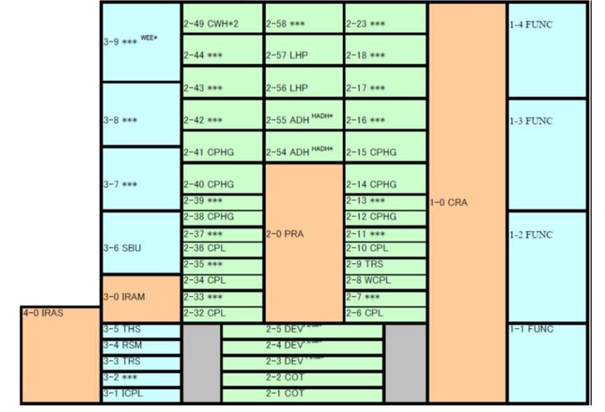
(2) Coater / (3) Developer systems, 12"
Single block for NSR S308
(4) Blocks interfaced:
Carrier
Process
Stepper interface main
Stepper interface sub
(4) Wafer transfer robot arms:
Carrier
Process
Stepper interface main
Stepper interface sub
(4) Cassettes FOUP Design
SECSI/II, HSMS and GEM Interface required IUSC
Interface is to NSR S308
(2) Coaters (COT)
(4-8) Resist nozzles with temperature control per coater
One touch filter
For resist and solvent
Mass flow controller
(3) Developers (DEV)
NLD Nozzles with temperature control per cup
(3) PRD Nozzles
Developer
One touch developer filter
Thermo Controller Unit (TCU) Inside track
(2) Adhesion Process Stations (ADH)
(5) Chill Plate Process Stations (CPL)
Transfer Chill Plate (WCPL)
(2) Low Temperature Hot Plate (LHP)
N2 Purge capability
(6) Precision Chilling Hot Plate Process Stations (CPHG)
Wafer Edge Exposure system (WEE)
Interface block
Single pincette wafer transfer with centering guides
For standard wafer arm and interface panel to accommodate
Buffer cassette, 3"-6"
Subcomponents:
Temperature
Humidity controller
(2) Chemical cabinets
AC Power box.
TEL / TOKYO ELECTRON Lithius provides an advanced and reliable lithographic processing equipment used to develop photoresist patterns. Photoresists are materials used in lithographic processes to produce patterns in materials such as metals, plastics, ceramics, semiconductors and others. TEL Lithius offers an integrated processing system that allows photoresists to be developed on a large variety of materials. Photoresists are applied to the surface of a material via spin coating, and are then exposed to light of various wavelengths and intensities in order to selectively remove or harden the photoresist. The resulting etched pattern is generated depending on the light exposure and crystallization of the photoresists. Photoresists can also be patterned using a photomask, which is a patterned light transmitting media, or a programmable computer generated pattern. This unit is designed to handle a wide range of materials including silicon wafers, glass plates, polymers, paper and textile products. The exposed substrate is then developed using a variety of solutions that remove or harden the exposed photoresist onto the substrate with high precision. The result is a patterned substrate with accurate features and a high surface quality. This machine features automated alignment and a unique film spreading mechanism that ensures that the photoresists are applied accurately and evenly to the substrate. It also features an innovative process chamber tool with adjustable exposure and constant temperature to create consistent results. The on-board asset controls also allow for a range of parameters to be set including exposure times, wavelength of light and shutter speed to create the most effective results. The model also includes a comprehensive monitoring equipment to ensure repeatable results. TOKYO ELECTRON Lithius photoresist system is designed to be one of the most reliable and advanced lithographic processing systems available that provides reliable and repeatable results. It is specifically designed to allow for automated processing of various materials with precision and reliable results.
There are no reviews yet


