Used TEL / TOKYO ELECTRON Lithius #9355520 for sale
URL successfully copied!
Tap to zoom


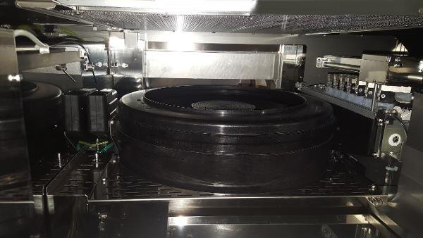
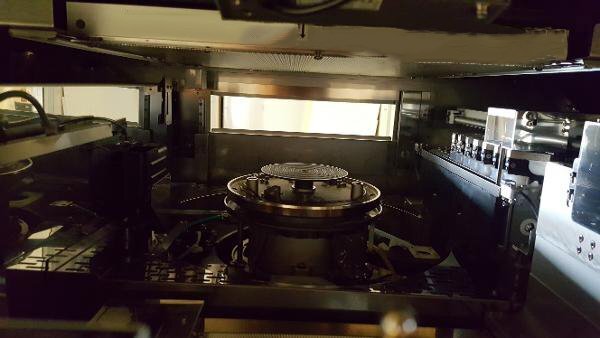
TEL / TOKYO ELECTRON Lithius is a photolithography equipment that uses a specialized photoresist coating to transfer device patterns onto a wafer or a substrate. Photolithography is a process of exposing a specific area of a thin layer of photoresist material to ultraviolet light, which causes the exposed material to become more chemically sensitive. This allows the chemical removal of the exposed material to form patterns in the photoresist layer. TEL Lithius photolithography system utilizes an advanced coating process to create intricate micro- and nanometer-scale features and patterns on a wide range of substrates. The first step in the photolithography process is to coat a substrate with a film of photoresist. A dispenser creates a uniform layer of photoresist on the substrate and automatically aligns the pattern to be created. The photoresist is exposed to ultraviolet light through a Complex Optical Unit (SITEX). The ultraviolet light that transmits through the mask is directed at the resist to create the desired pattern. Subsequently, the exposed resist is developed, removing the exposed material to form patterns. The developed substrate is then of-processed, washed, and the patterns are photoresist processes are reduced even further with the SITEX machine. In addition to creating micro- and nanometer-scale features, TOKYO ELECTRON Lithius photolithography tool also enables the use of high-resolution materials to create high-density device patterns. The asset also employs advanced automation and process monitoring systems for quality control as well as a wide range of substrates and resists to effectively reduce costs. The photolithography process with Lithius is essential for making and patterning semiconductor devices. Photoresists permits very rapid and precise control over the amount of material removed, making it the main tool for fine patterning. The model provides control of feature size and other critical lithographic parameters that are required for creating intricate semiconductor devices. The equipment is used for the fabrication of transistors, integrated circuits, memory chips, complete microprocessors, and other types of electronic components.
There are no reviews yet


