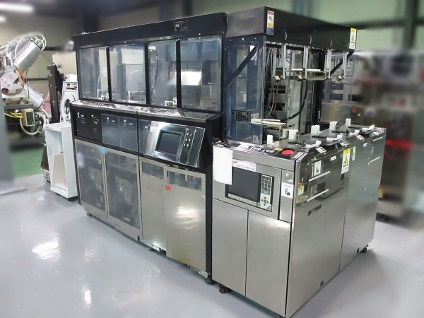
Used TEL / TOKYO ELECTRON Mark 7 #9214147 for sale
It looks like this item has already been sold. Check similar products below or contact us and our experienced team will find it for you.
Tap to zoom


Sold
ID: 9214147
Wafer Size: 8"
Vintage: 1996
Coater / (2) Developers system, 8"
AD
(4) HP
(3) CP
1996 vintage.
TEL / TOKYO ELECTRON Mark 7 is a photoresist equipment used in the photolithography step of semiconductor device fabrication. The system is composed of a photoresist spinning unit, a multi-spot exposure station, and an auto thermal protection unit. The photoresist spinning unit is used to spin photoresist-coated wafers at precisely controlled speeds in order to achieve uniform spin rates across the wafers. The multi-spot exposure station employs multi-spot laser beams to simultaneously expose the photoresist-coated wafers without the need for conventional mask alignment techniques, enabling increased throughput levels. Additionally, the exposure station is equipped with an alignment unit that utilizes both lasers and cameras to precisely focus and align the pattern of the exposure images on the wafers. Finally, the auto thermal protection unit is an integrated heat control machine that is used to prevent overheating of the wafers during the resist spinning and exposure processes. In operation, TEL MARK7 begins with the photoresist spinning unit. After the photoresist has been spun onto the wafers, the multi-spot exposure station illuminates the wafers in order to etch the desired features into the resist. The alignment tool of the exposure station is calibrated to quickly and accurately align the exposure masks to each individual wafer, allowing for fast processing rates. Finally, the auto thermal protection unit monitors the temperature of the wafers in order to ensure the maximum thermal protection of the photoresist throughout the process. Overall, TOKYO ELECTRON MARK-7 is a powerful and reliable photolithography asset that enables semiconductor manufacturers to quickly and accurately processes wafers, while also providing the highest level of thermal protection for the photoresist during the fabrication process. With its advanced laser-based exposure mechanisms and precision alignment model, MARK7 is an ideal solution for meeting the high throughput and accuracy requirements of modern semiconductor device manufacturing.
There are no reviews yet