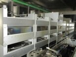
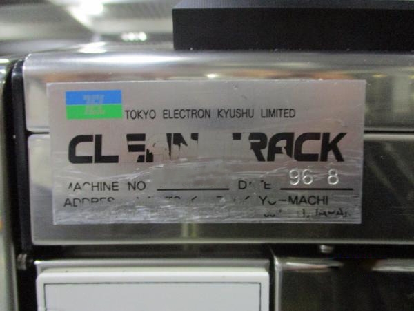
Used TEL / TOKYO ELECTRON Mark 7 #9215816 for sale
URL successfully copied!
Tap to zoom








ID: 9215816
Wafer Size: 8"
Vintage: 1996
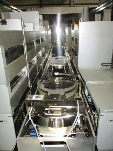
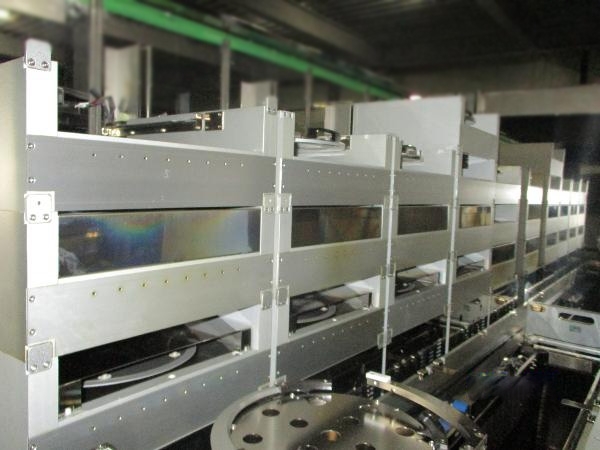
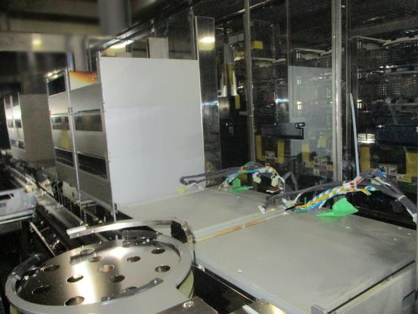
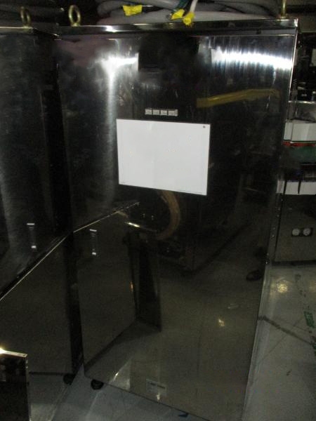
Coater / Developer system, 8"
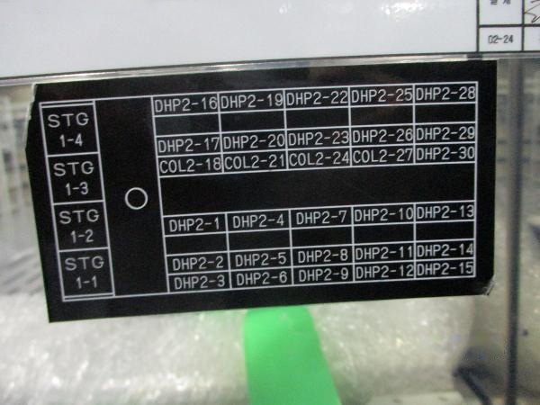
(8) DHP
(4) CP
1996 vintage.
TEL / TOKYO ELECTRON Mark 7 is a photoresist equipment that provides advanced lithographic exposure solutions for semiconductor fabrication and production. It is an advanced piece of equipment that maximizes process control and image placement accuracy. TEL MARK7 utilizes optical proximity correction (OPC) to create highly precise optical lithography patterns on the semiconductor wafers. The OPC algorithms allow for the precise placement of microscopic features down to the nanometer level. This is necessary for successful fabrication of highly intricate IC designs used in modern semiconductor products. The machine also has a highly precise motion system, with motion control sensors that deliver high-accuracy positioning and velocity feedback. The scanning unit of TOKYO ELECTRON MARK-7 operates in both slow and fast modes, allowing for precise alignment and positioning of the micron scale patterns on the surface of the wafer. In addition, the same machine certified by the International Technology Roadmap for Semiconductors (ITRS) and the Semiconductor Equipment and Materials International (SEMI) standards. TEL MARK-7 also features a patented in-situ wafer clamping tool. This enables tight and uniform clamping of the wafer to ensure better wbstrat placement during the lithography process. This helps prevent misalignment which could cause errors in the lithography patterns. TOKYO ELECTRON MARK7 is equipped with the state-of-the-art light detector, which can accurately measure the light intensity of the optical lithography pattern on the wafer. This detector helps maintain the perfect exposure conditions for a precise pattern transfer. In addition, the machine includes other advanced features such as exposure turbulence monitor, topography monitor, and image registrationverification asset, which further assist with ensuring precise exposure conditions and alignment during operations. These features help maintain precise and repeatable fabrication results. Finally, the machine also includes an automated reticle exchange model that saves time and effort when switching between different lithography patterns. This equipment allows the user to switch between the different patterns with the press of a single button. Clearly, TEL / TOKYO ELECTRON MARK-7 is an advanced and incredibly precise piece of equipment that provides advanced lithographic exposure solutions for semiconductor fabrication and production. Its precise motion system, in-situ wafer clamping unit, light detection machine, and other features make it an excellent tool for ensuring precise and repeatable fabrication results.
There are no reviews yet

