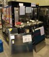
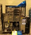
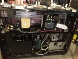
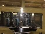
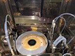
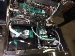
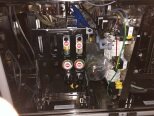
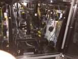
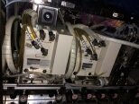
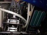
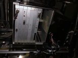
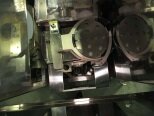
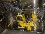
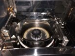
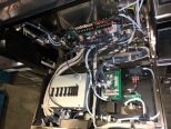
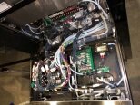
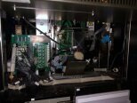
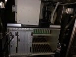
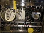
Used TEL / TOKYO ELECTRON Mark 7 #9239701 for sale
URL successfully copied!
Tap to zoom


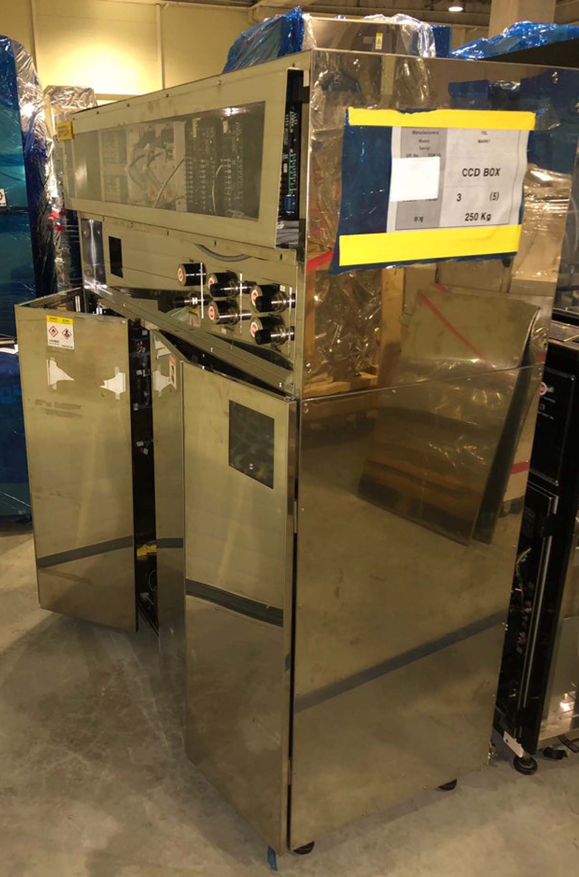

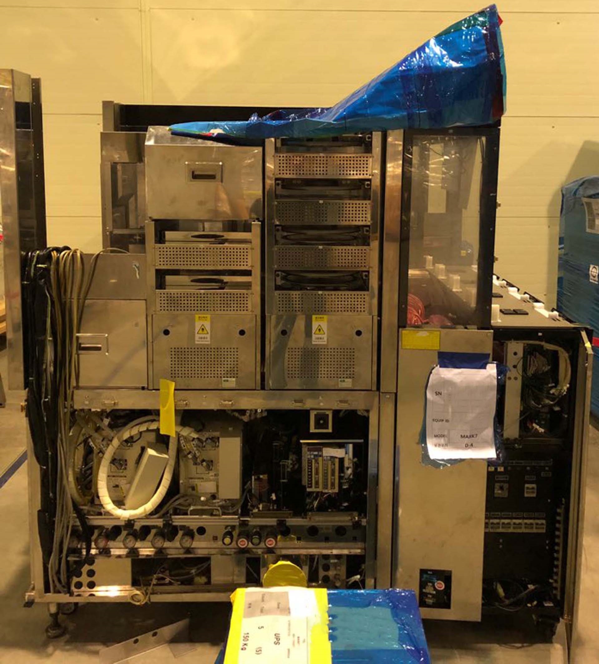

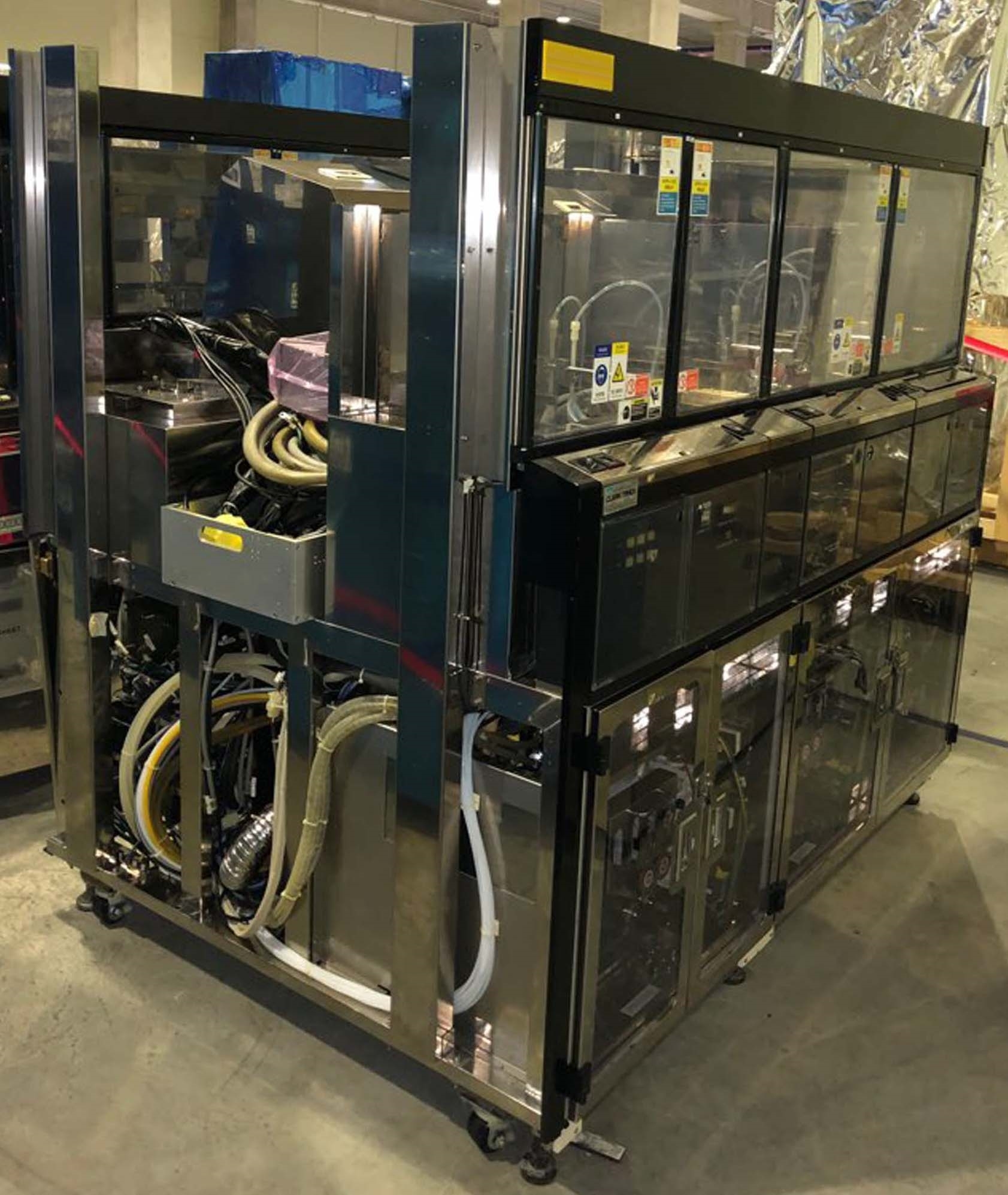











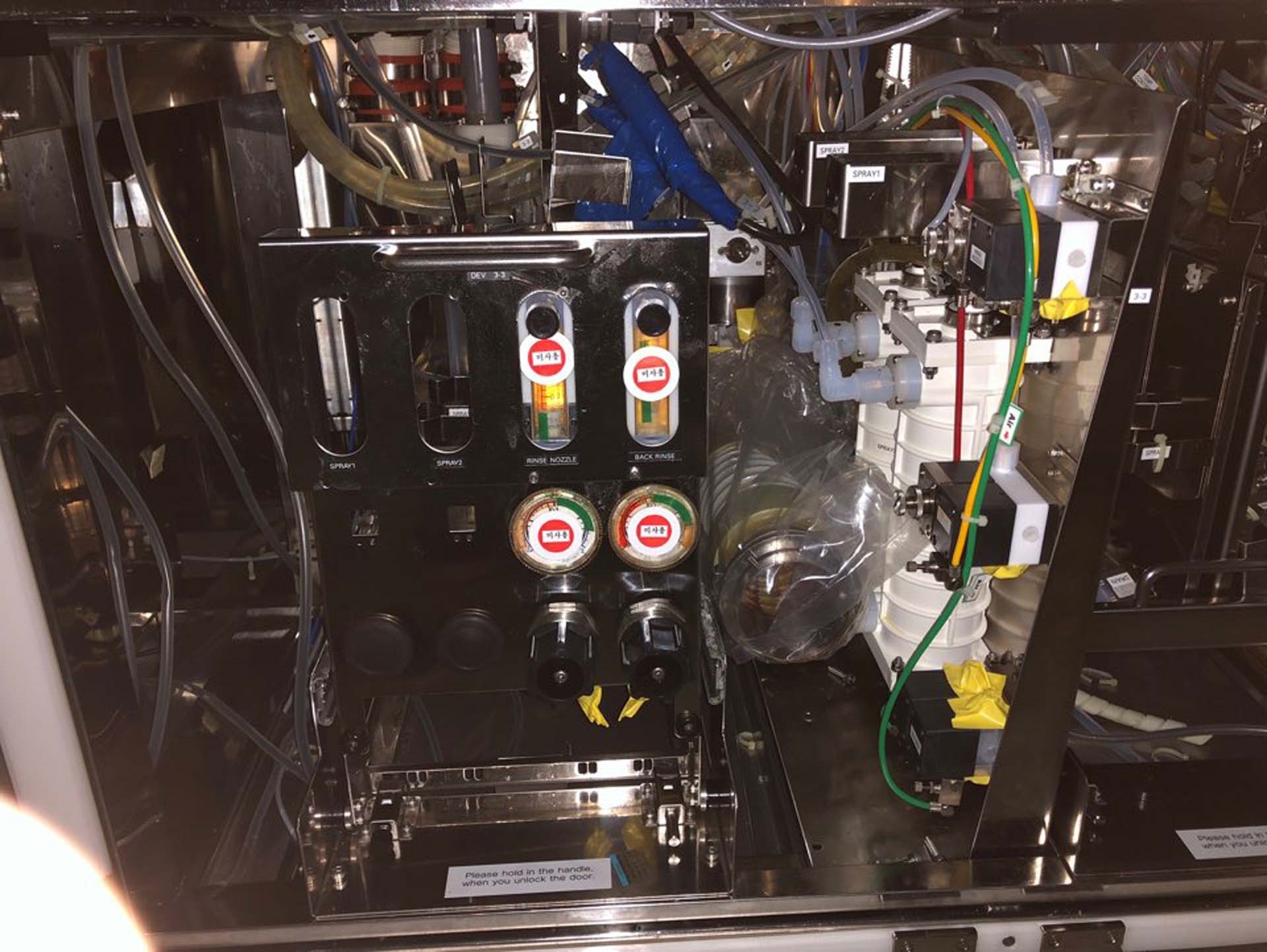


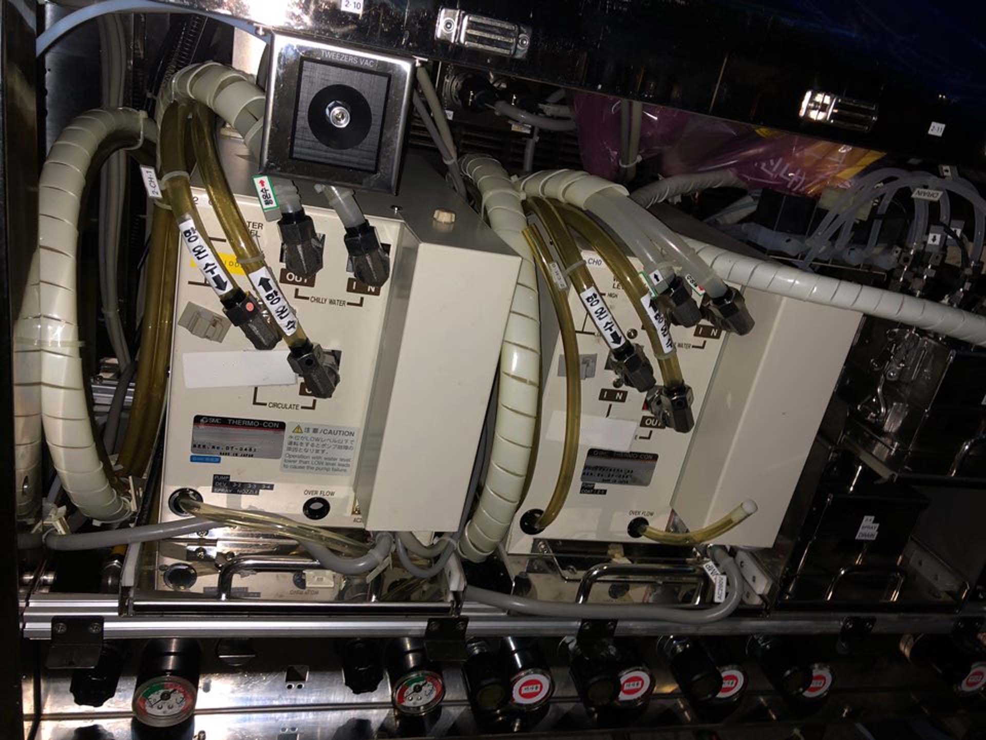

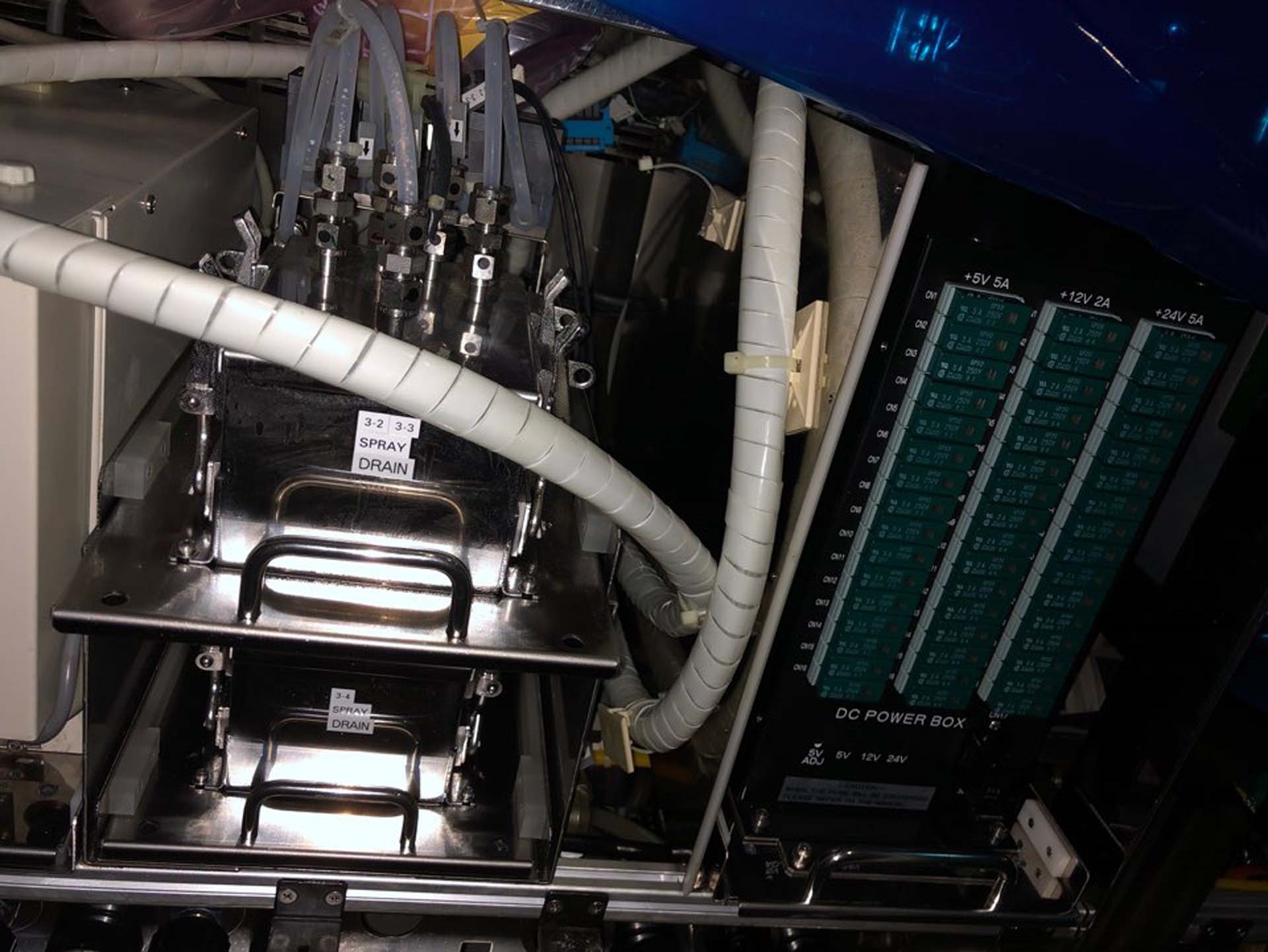

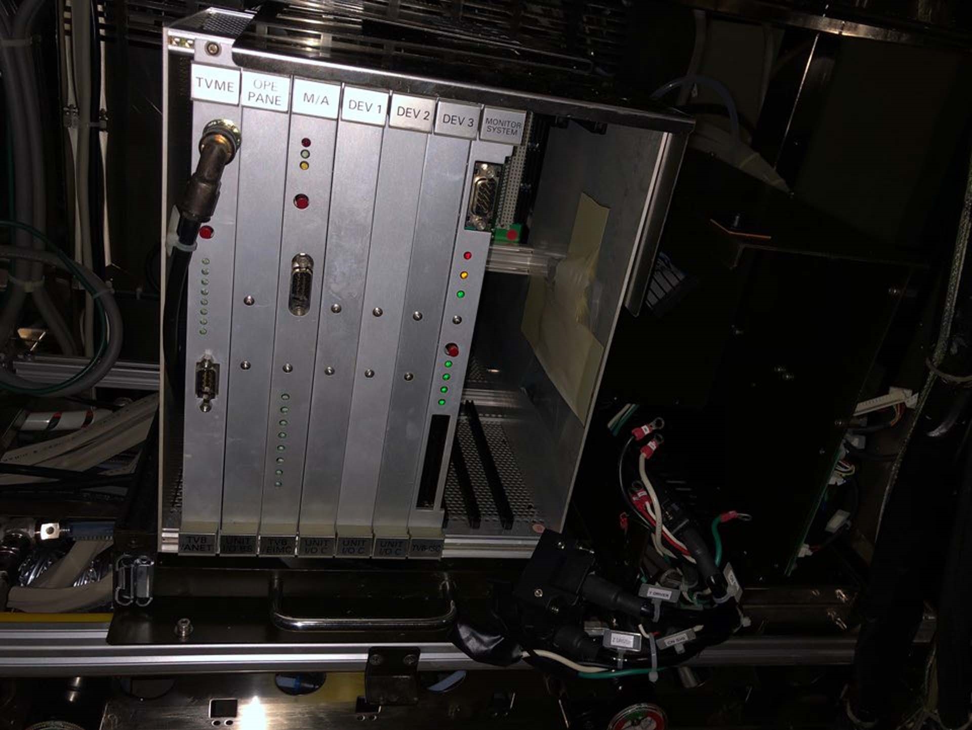





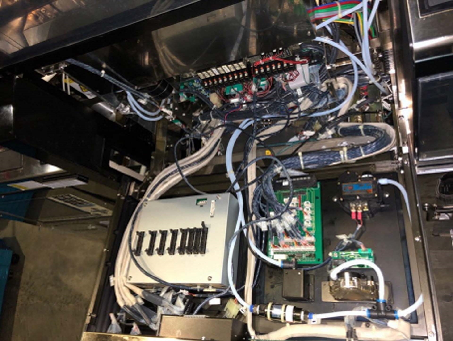


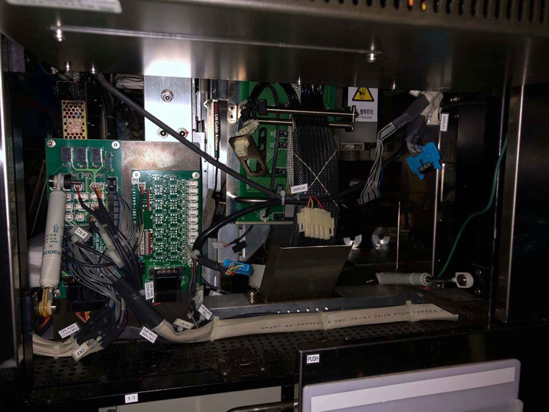

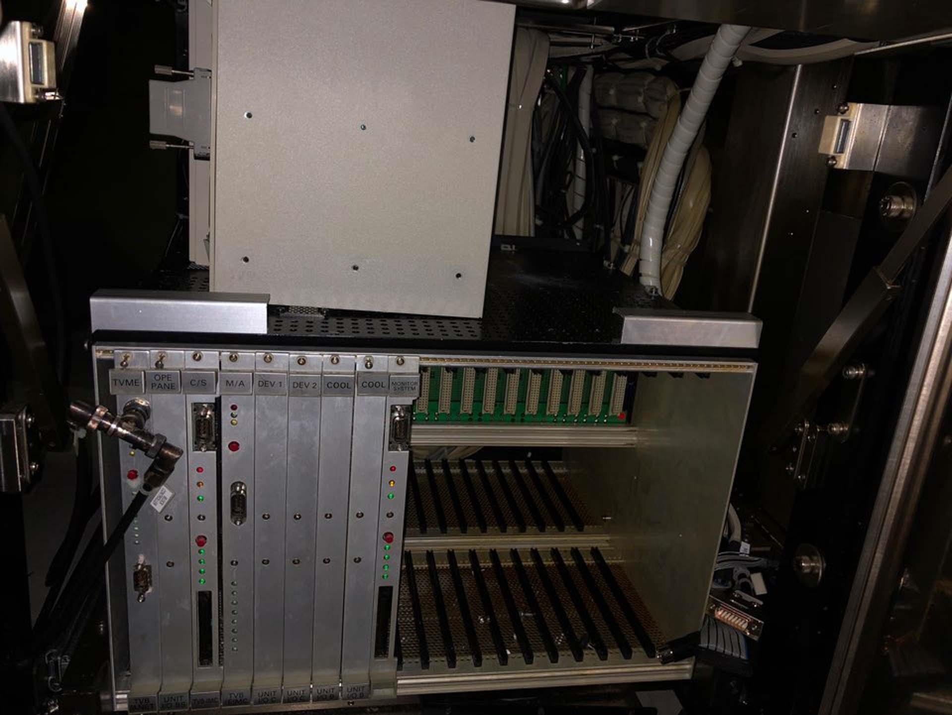


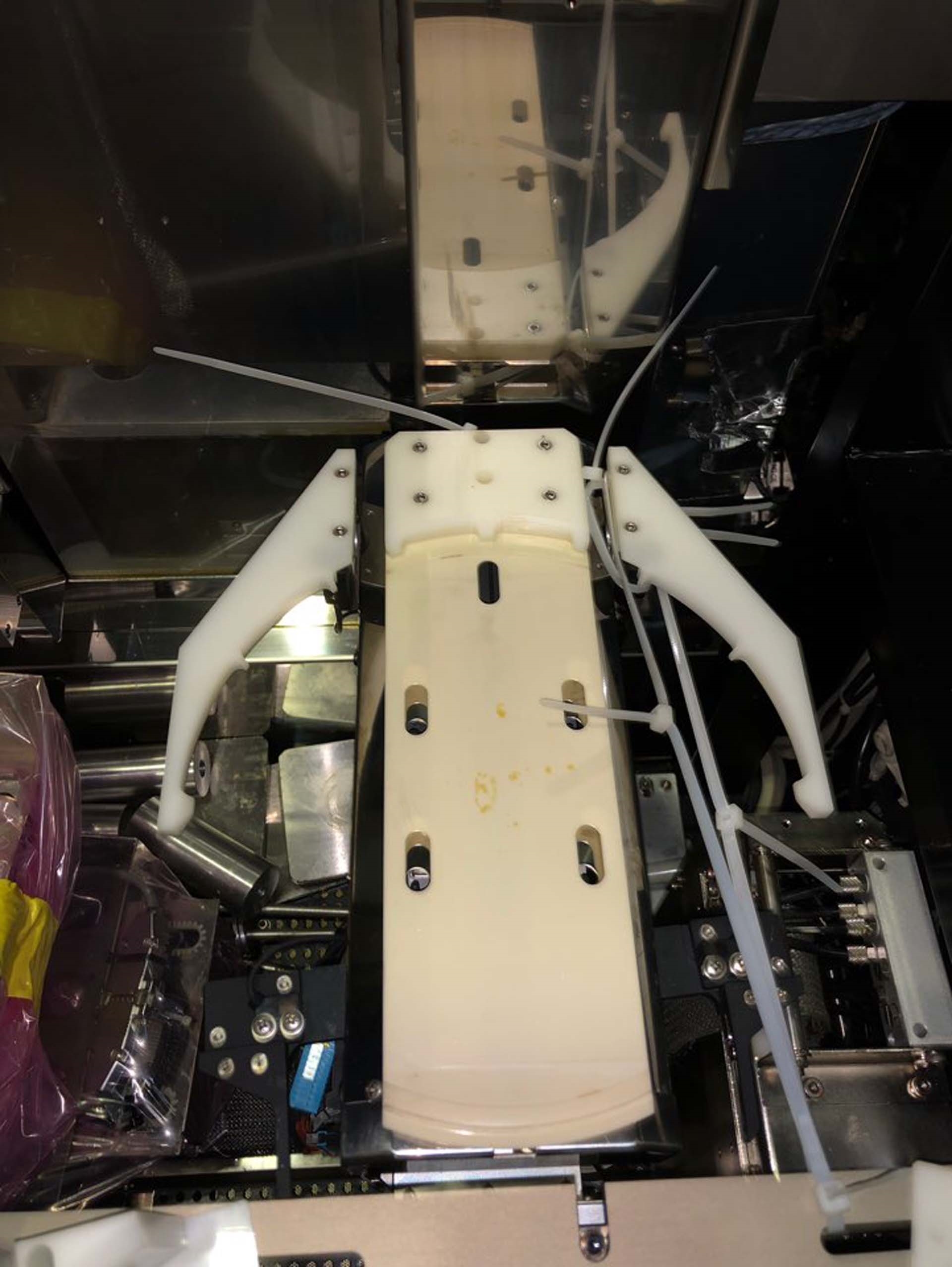


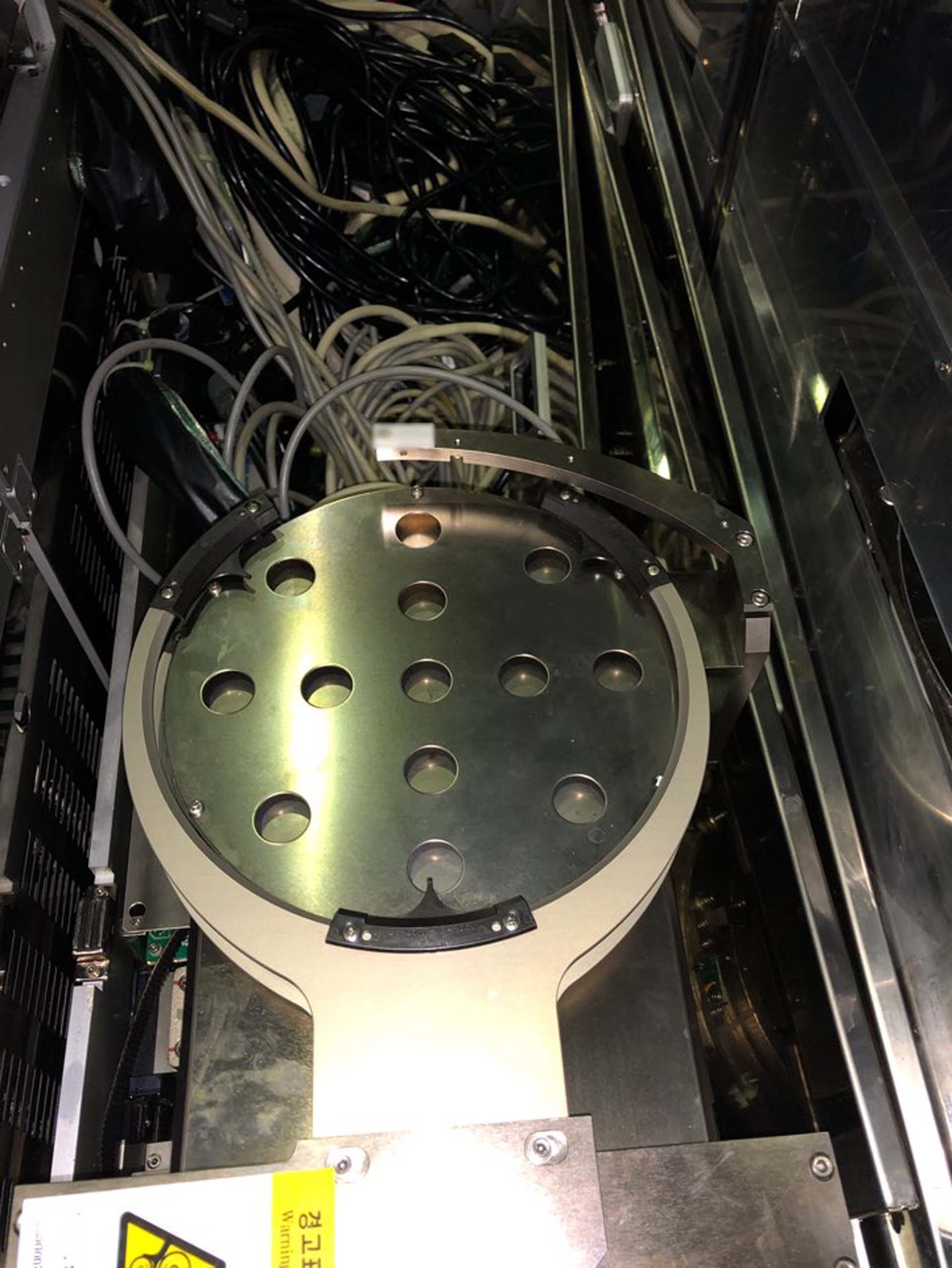


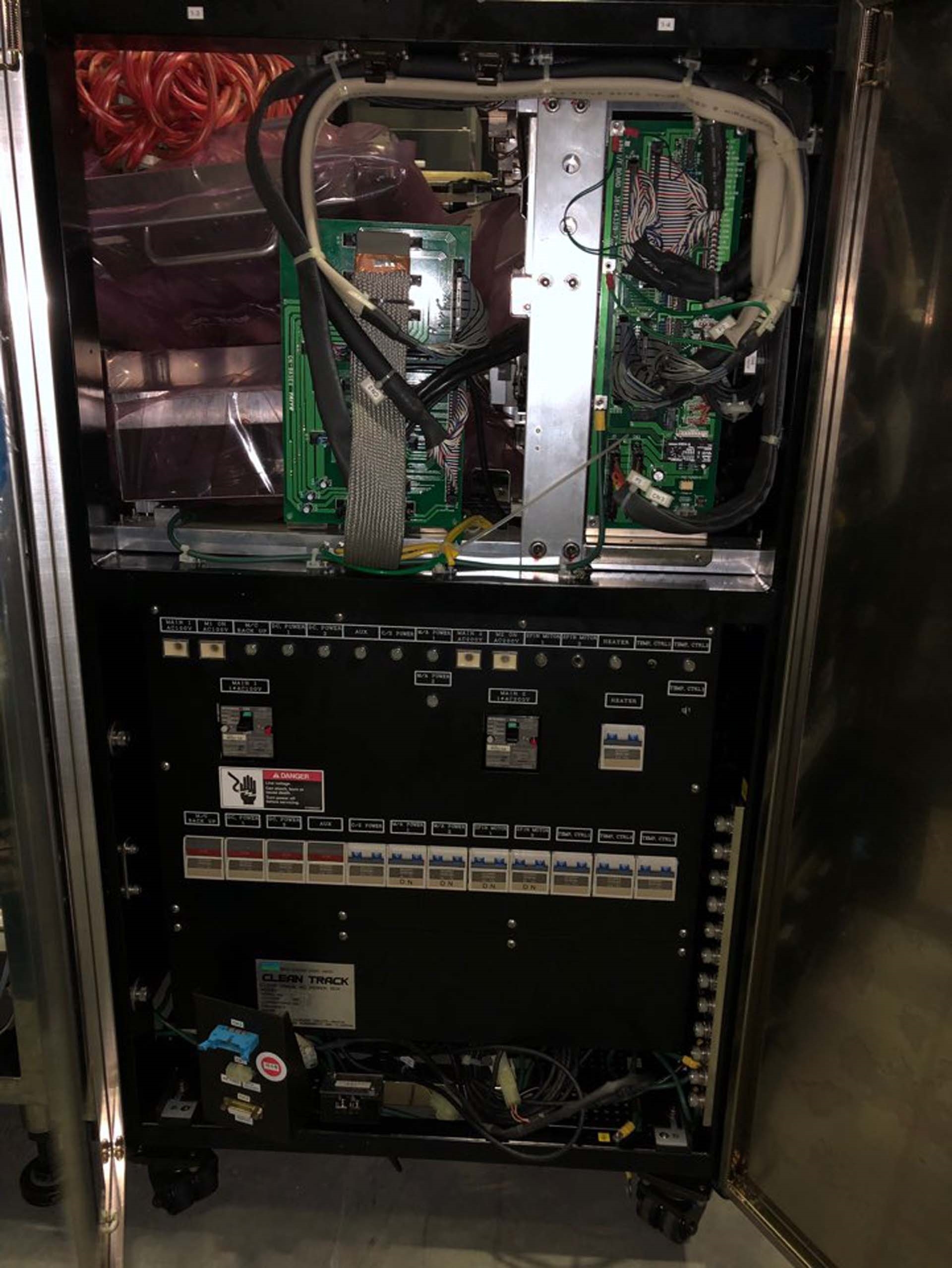



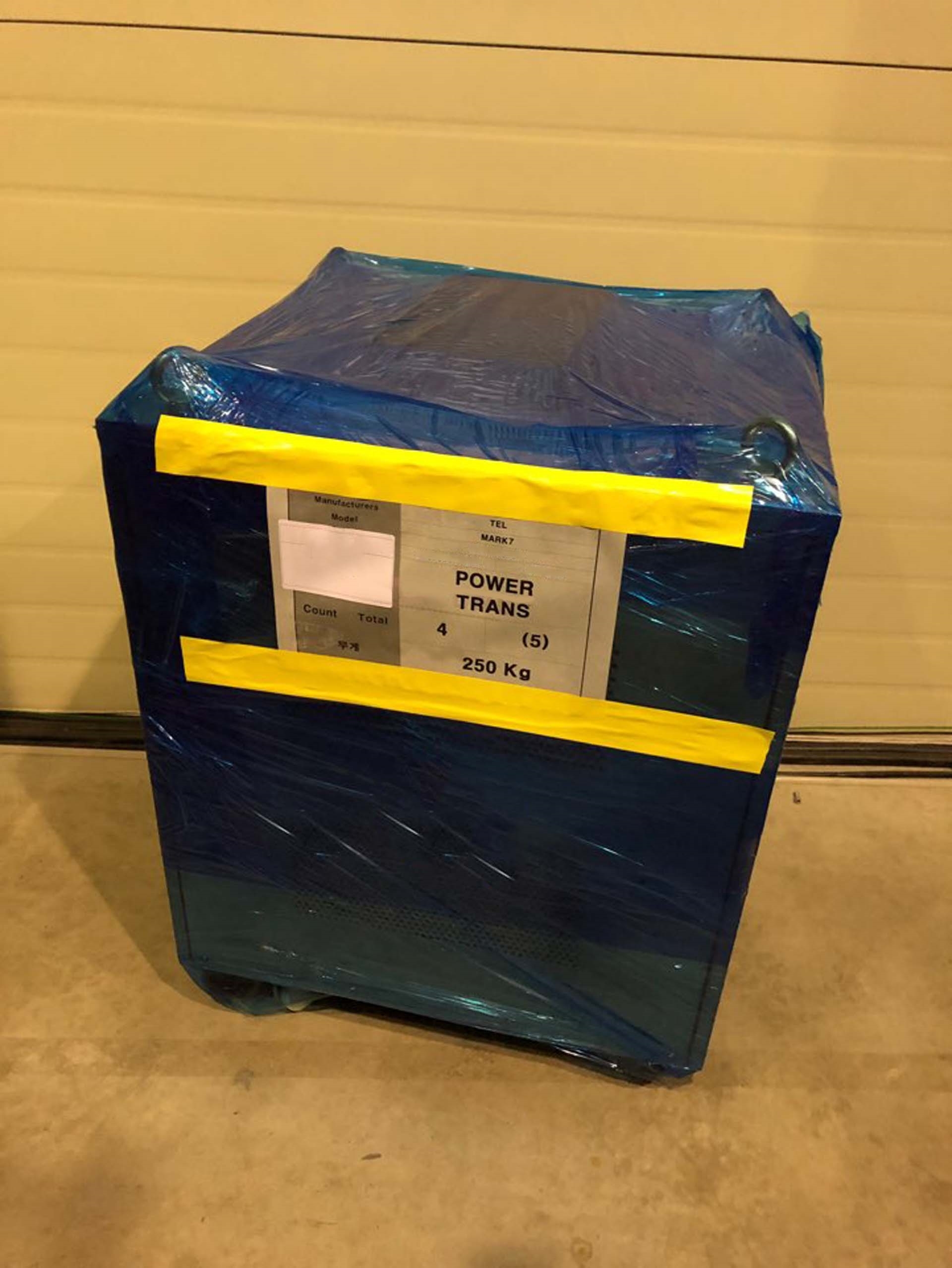


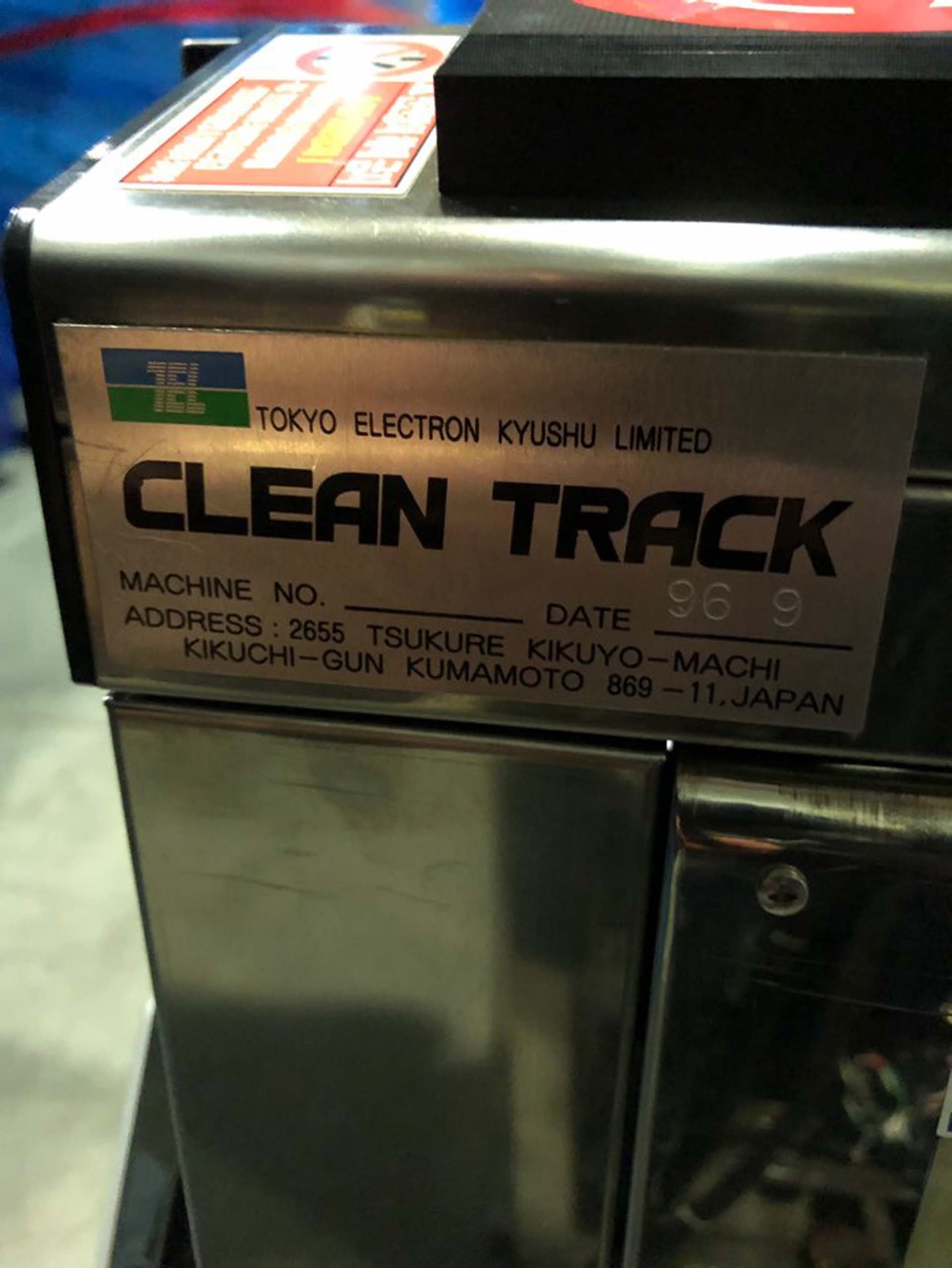

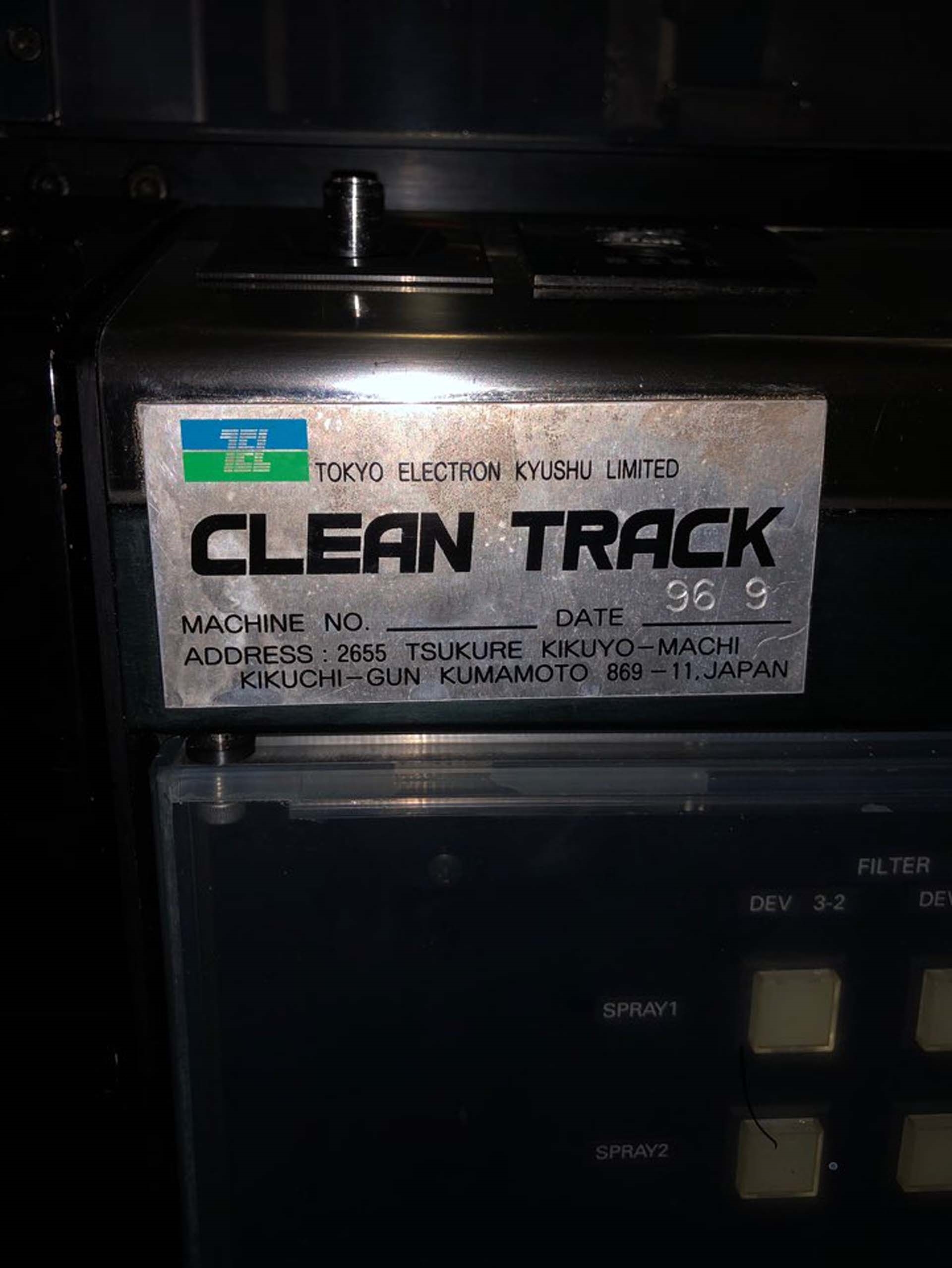

ID: 9239701
Wafer Size: 8"
Vintage: 1996
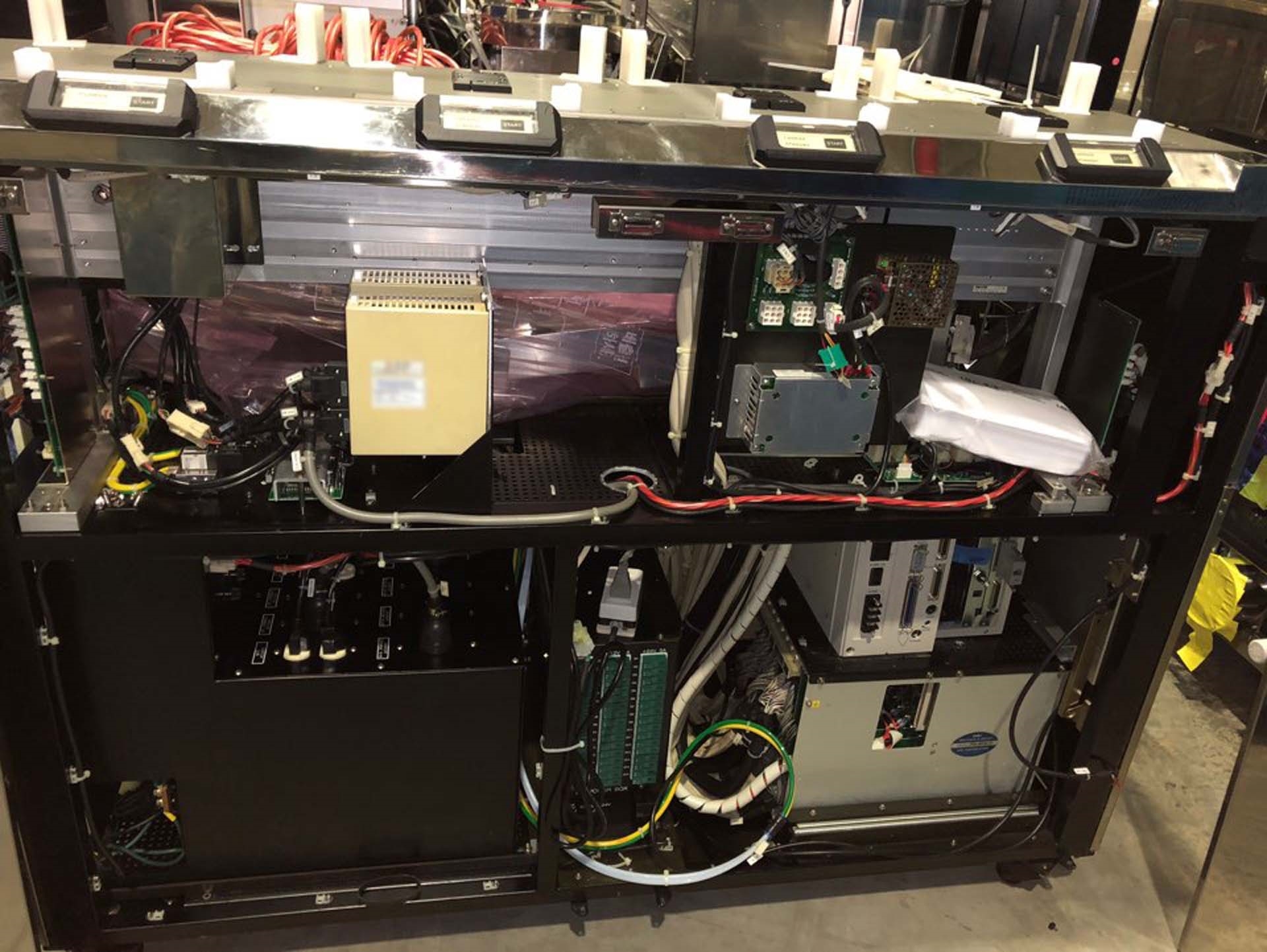
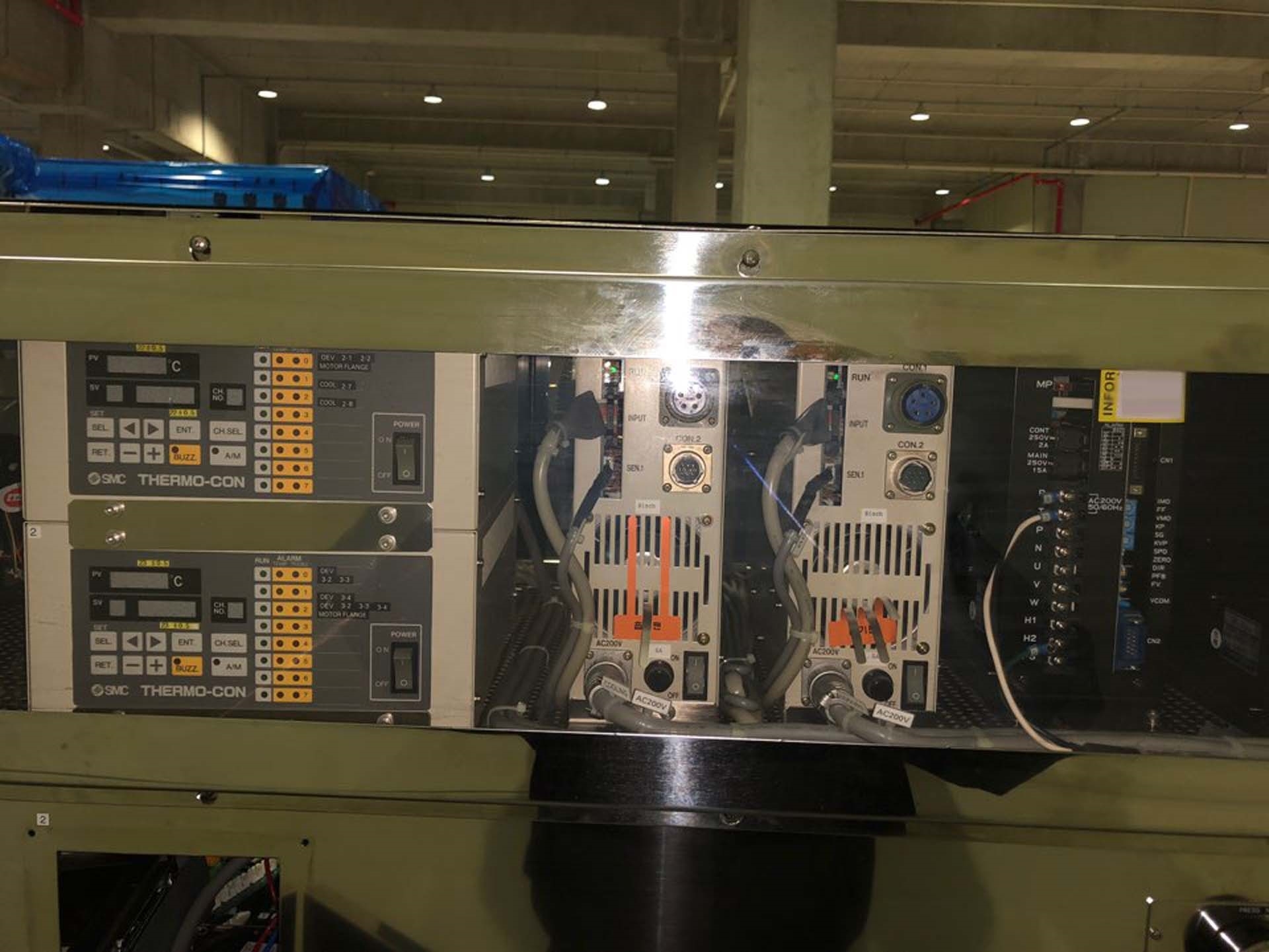
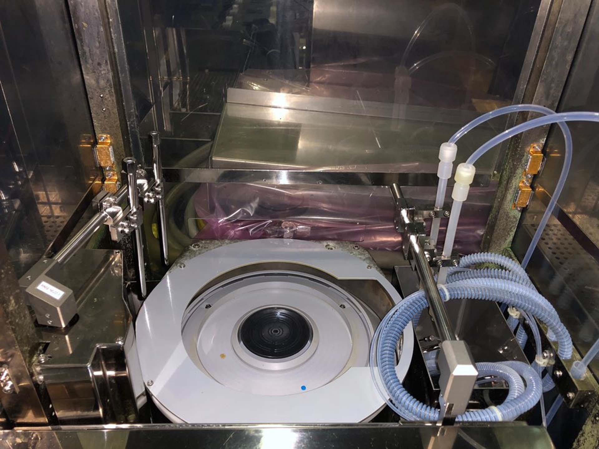
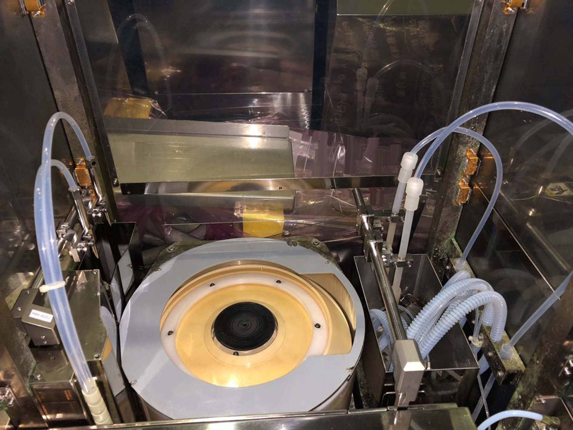
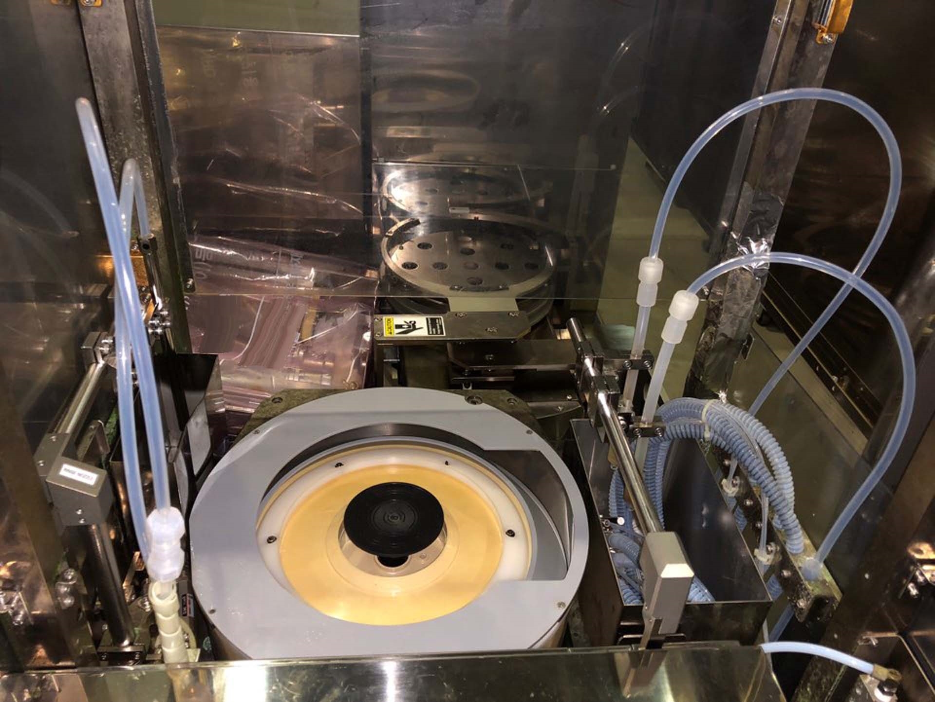
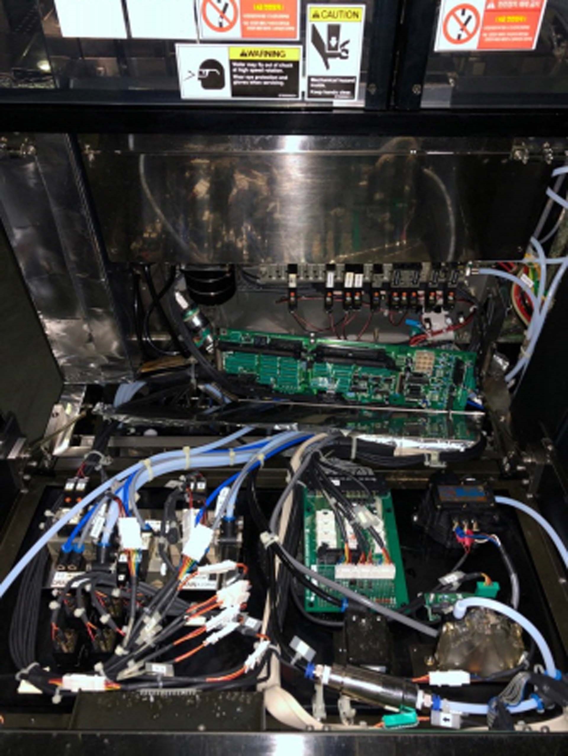
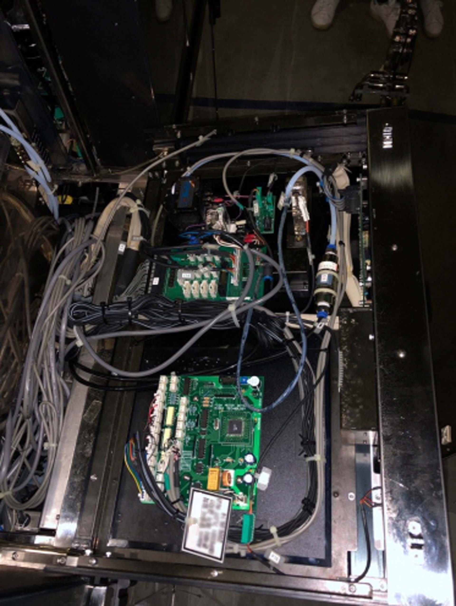
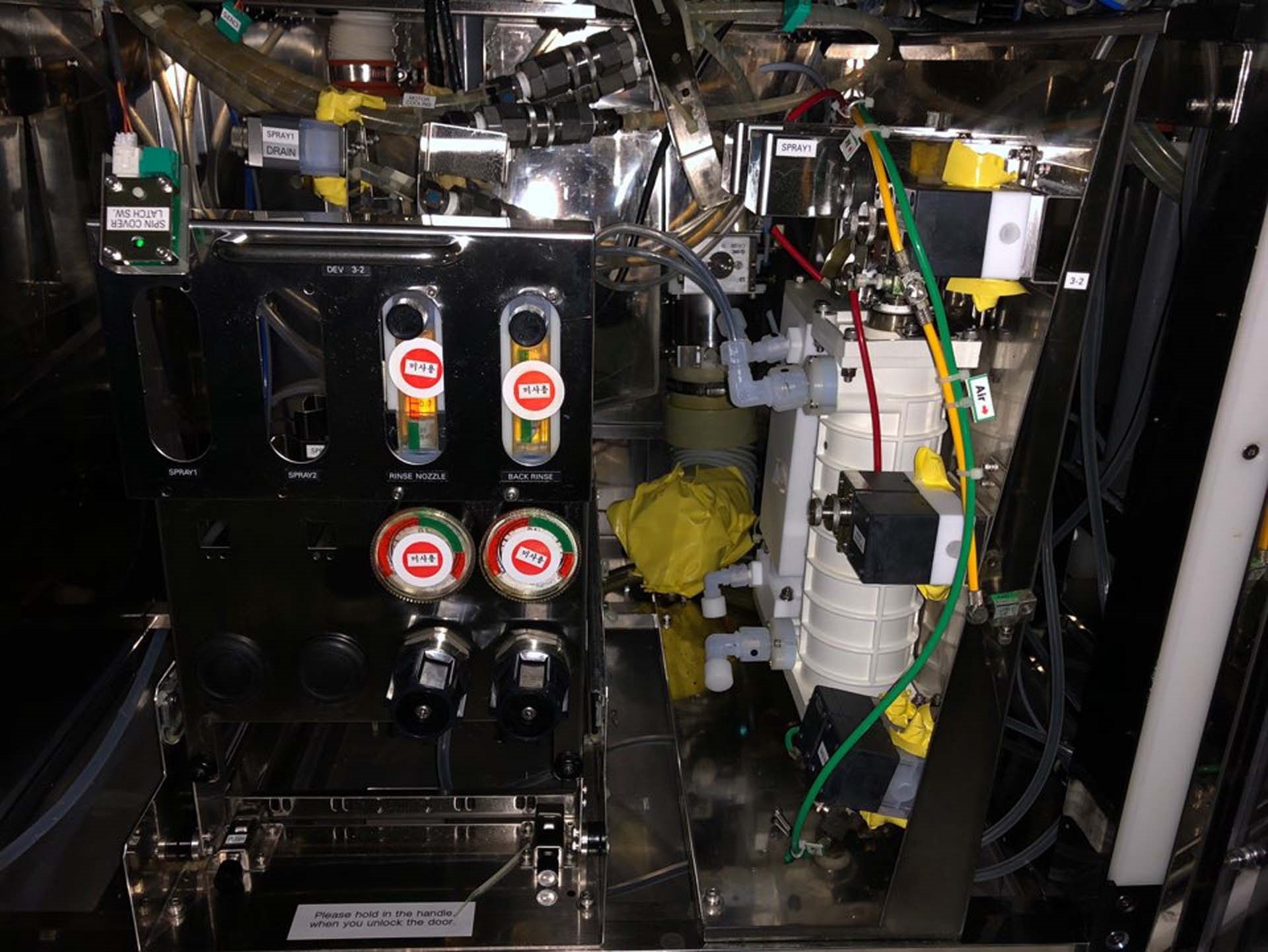
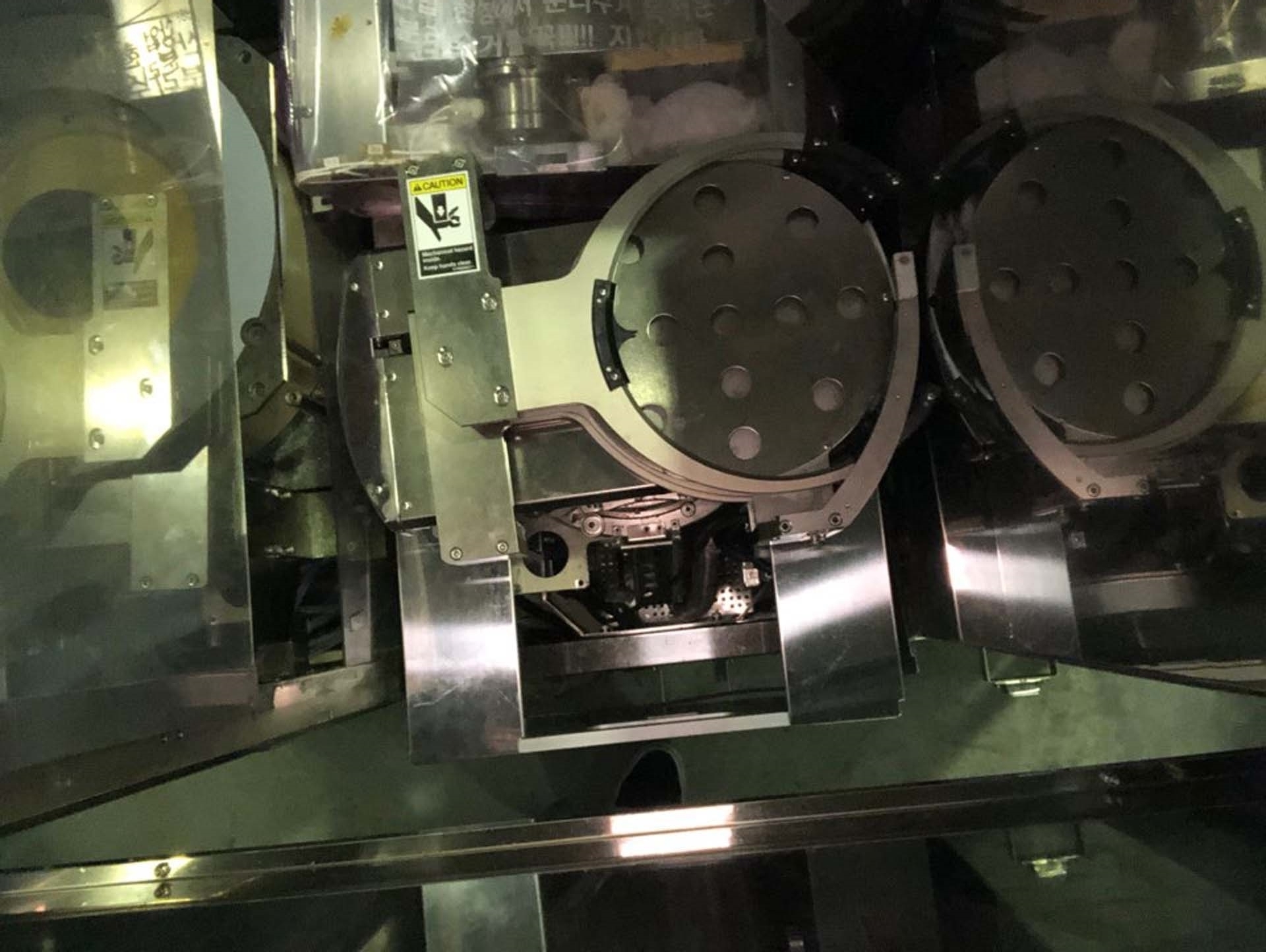
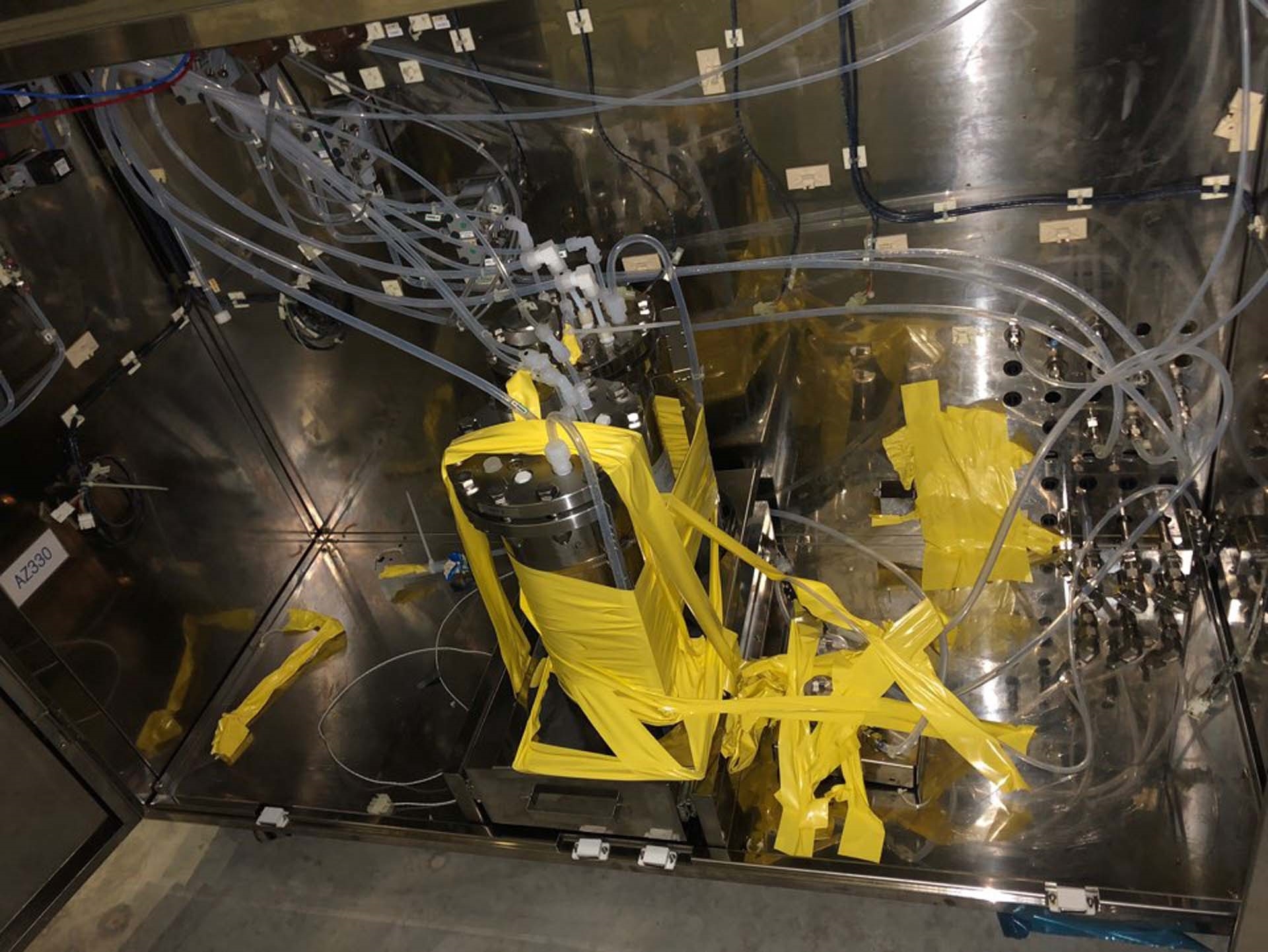
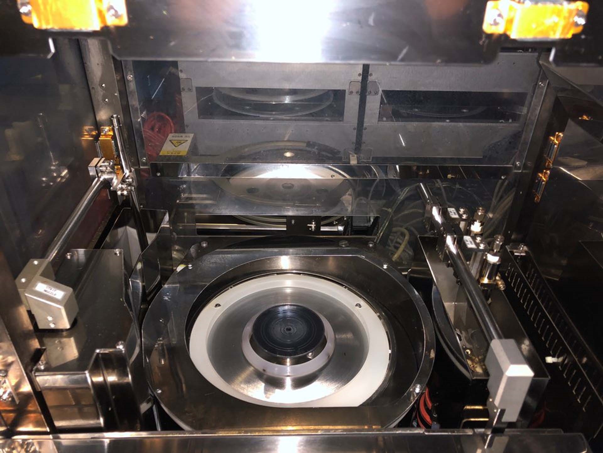
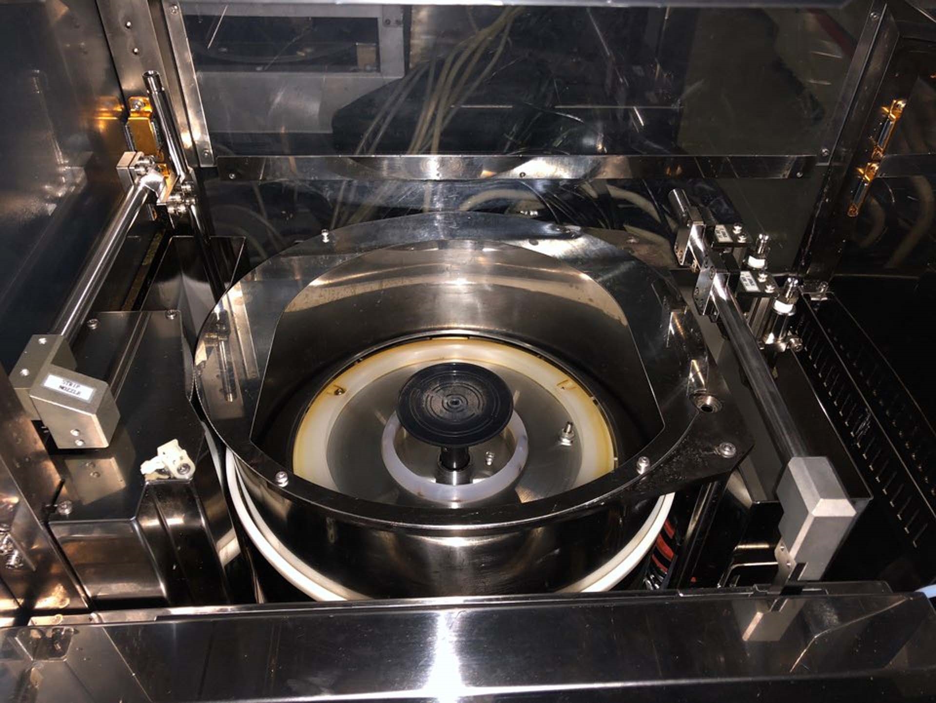
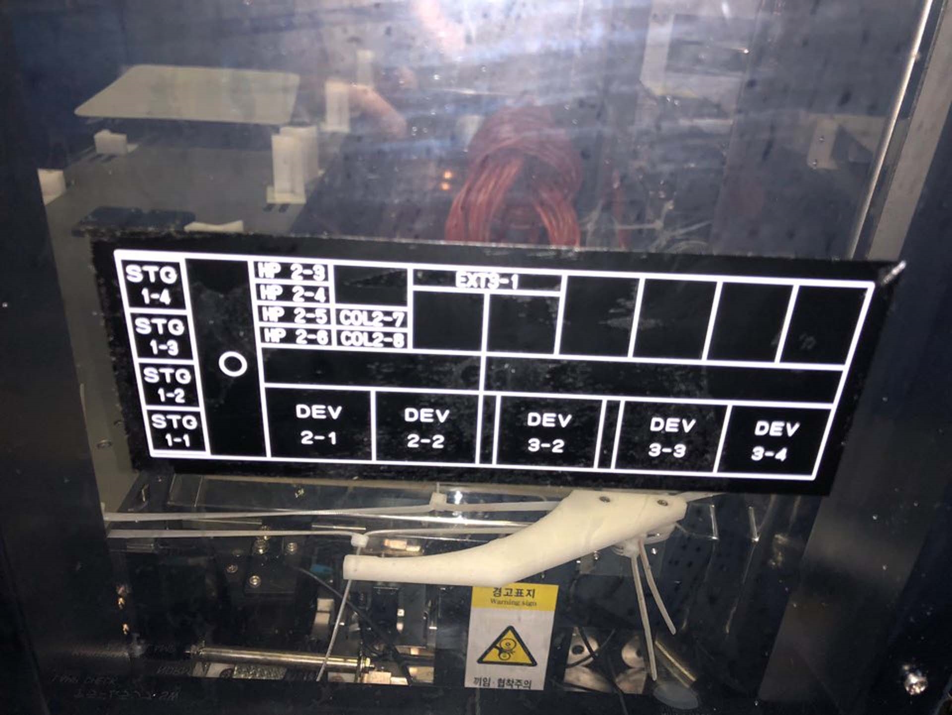
(2) Coater / (3) Developer system, 8"
Automation component: HSMS
Inline flow: Right
1996 vintage.
TEL / TOKYO ELECTRON Mark 7 photoresist equipment is a high-tech photolithography system designed for semiconductor manufacturing processes. TEL MARK7 unit is able to pattern and expose a variety of photoresists at extremely precise resolutions and is employed in several advanced stages of semiconductor manufacture. At the center of TOKYO ELECTRON MARK-7 machine is the ALTUS Exposure tool, which provides a selection of lasers and halogen lamps to expose photoresists of different types and sensitivities. Also included is an extended range of high-resolution alignment and inspection capability. The ALTUS Exposure asset 's open-loop software allows for patterning of up to 256 layers of various types of photoresists. The model can precisely define and adjust exposure boundaries according to the type of photoresist being used. With this capability, exposure time can be changed and optimized for each layer. The ALTUS Resolution Patterning Technology ensures exact placement of every feature, while providing the highest resolution possible. Mark 7 equipment is also able to perform ECRIS (Enhanced Critical Resolution Imaging System) imaging using BEAMER (high resolution imaging by means of electron beam). Advanced defect detection features in MARK-7 unit are provided by the TELECISAS (TELETron™ Machine for Advanced Inspection and Simulation). TELECISAS features include state-of-the-art progressive defect detection algorithms and a comprehensive database with quality control information. In addition to MARK7 tool's high-precision exposure capabilities, its data and materials management capabilities are equally impressive. All essential information is data-driven, making it easy to control the production process. Information is monitored and collected with intelligent data mining and analysis. The materials management asset covers every aspect of the process, from raw materials to finished products, and allows for detailed stock and ordering control. TEL Mark 7 model is a highly advanced photolithography solution, capable of providing high resolution, precision, and quality control. It is designed to facilitate the introduction of advanced semiconductor manufacturing processes while limiting expenses and improving productivity.
There are no reviews yet
