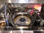
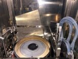
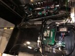
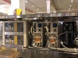
Used TEL / TOKYO ELECTRON Mark 7 #9241222 for sale
URL successfully copied!
Tap to zoom
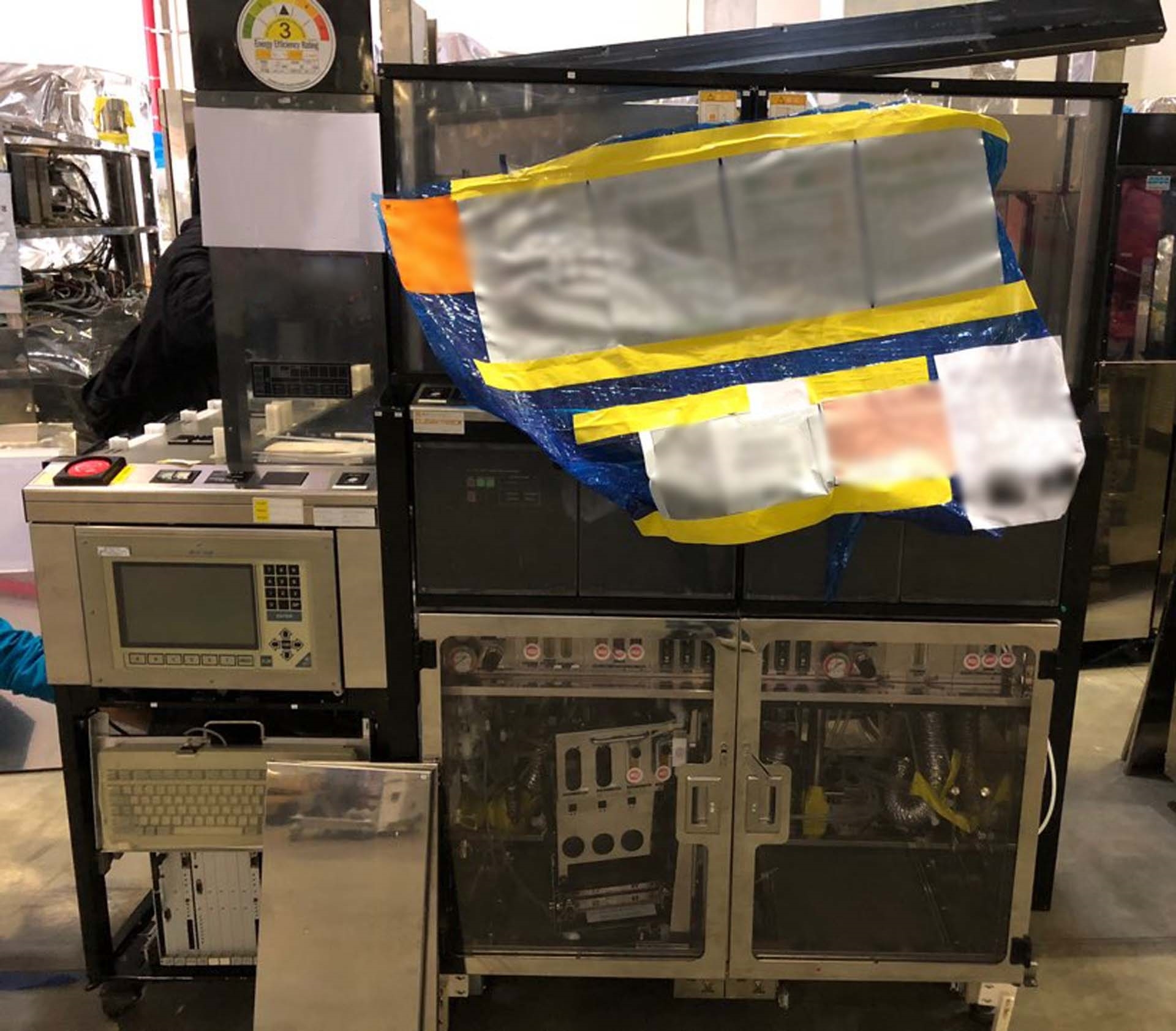

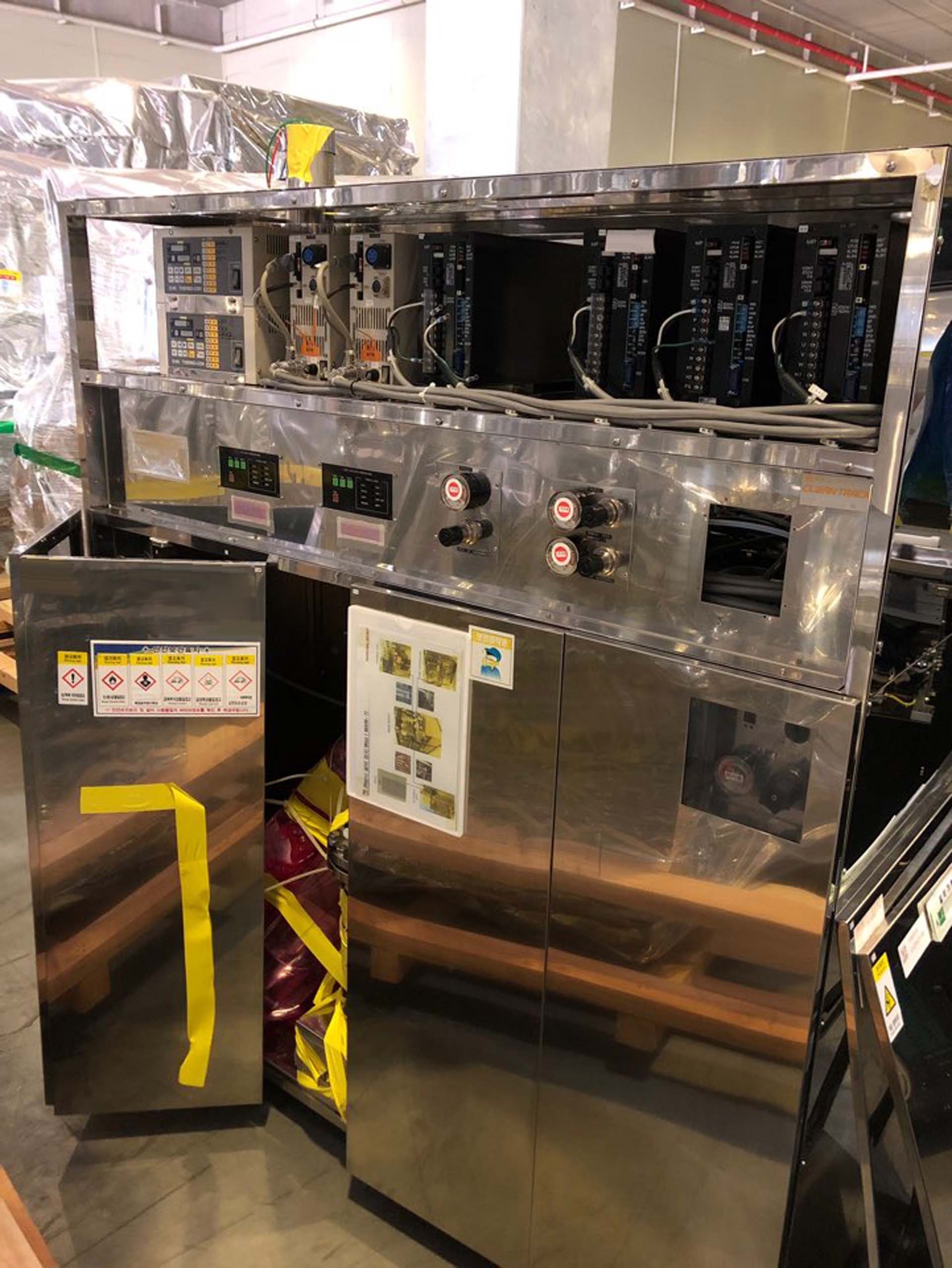


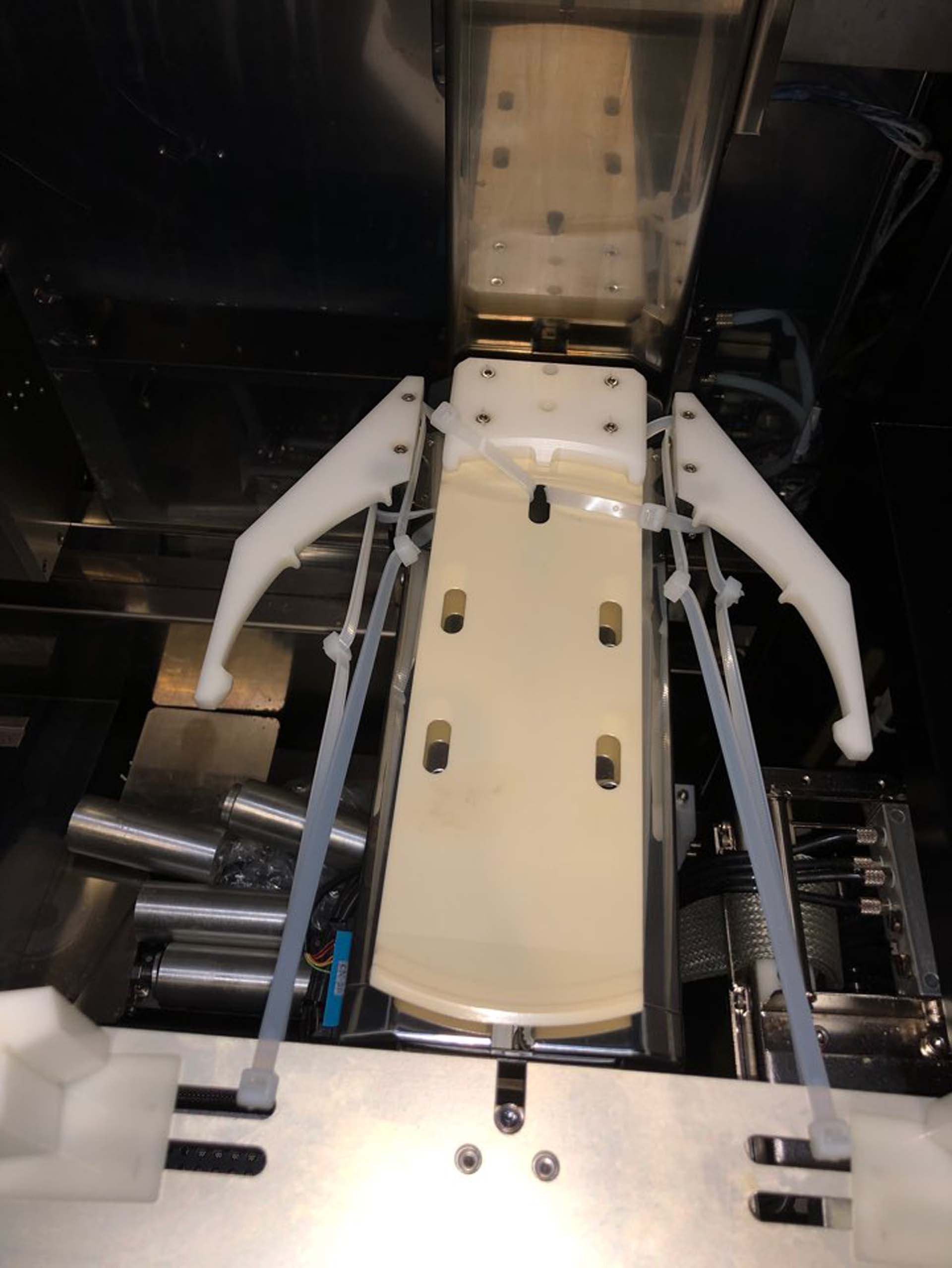

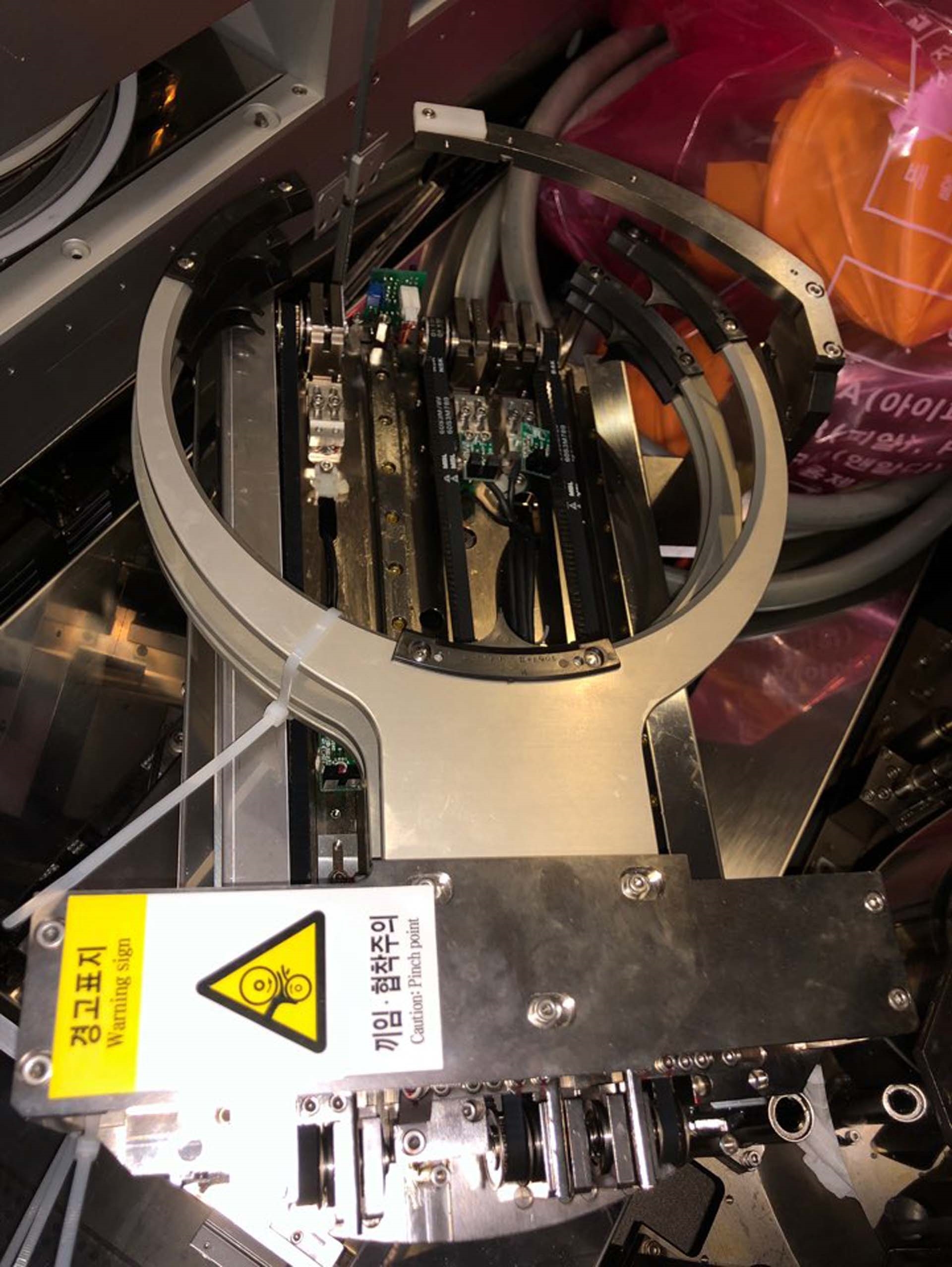

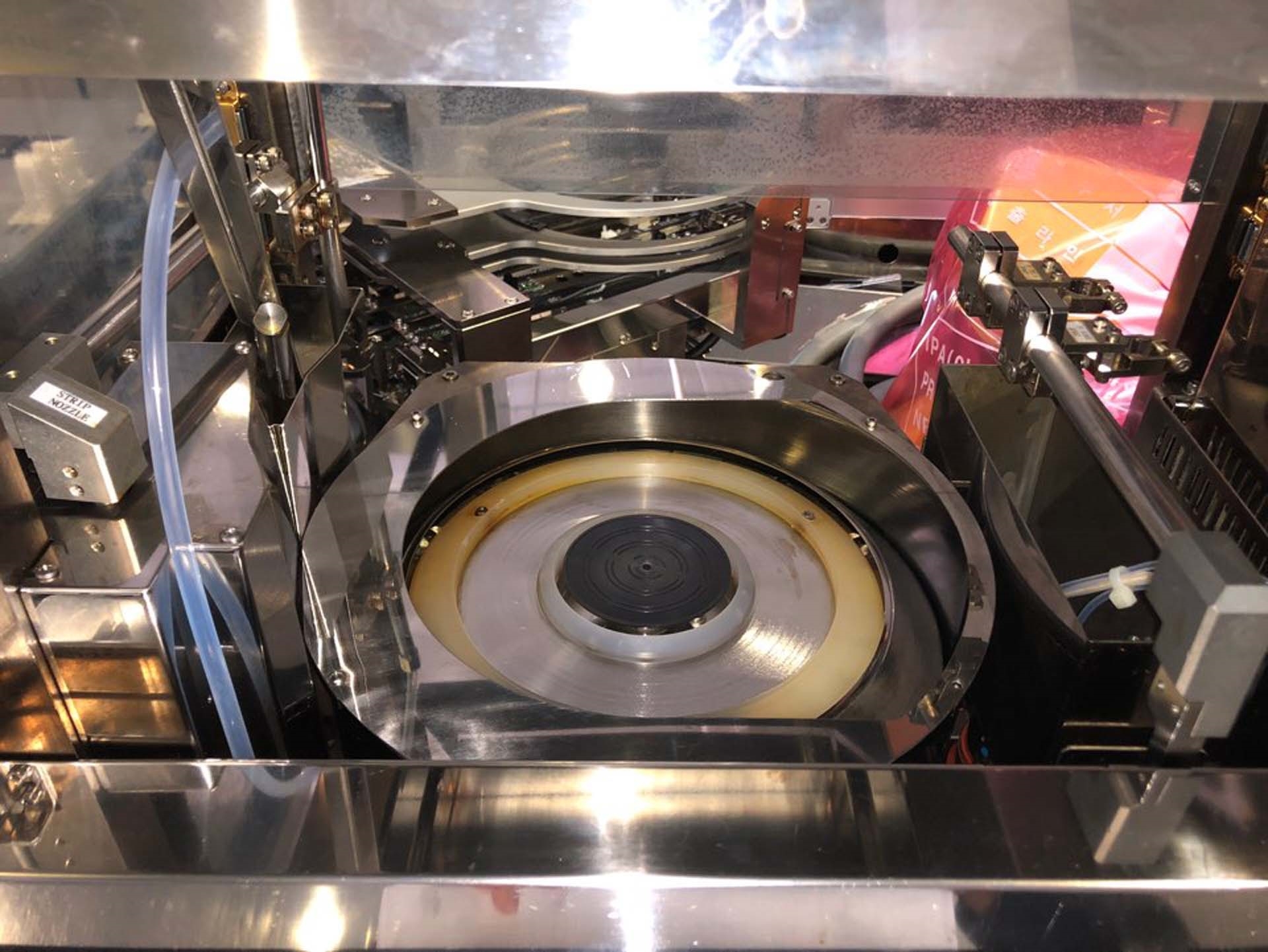

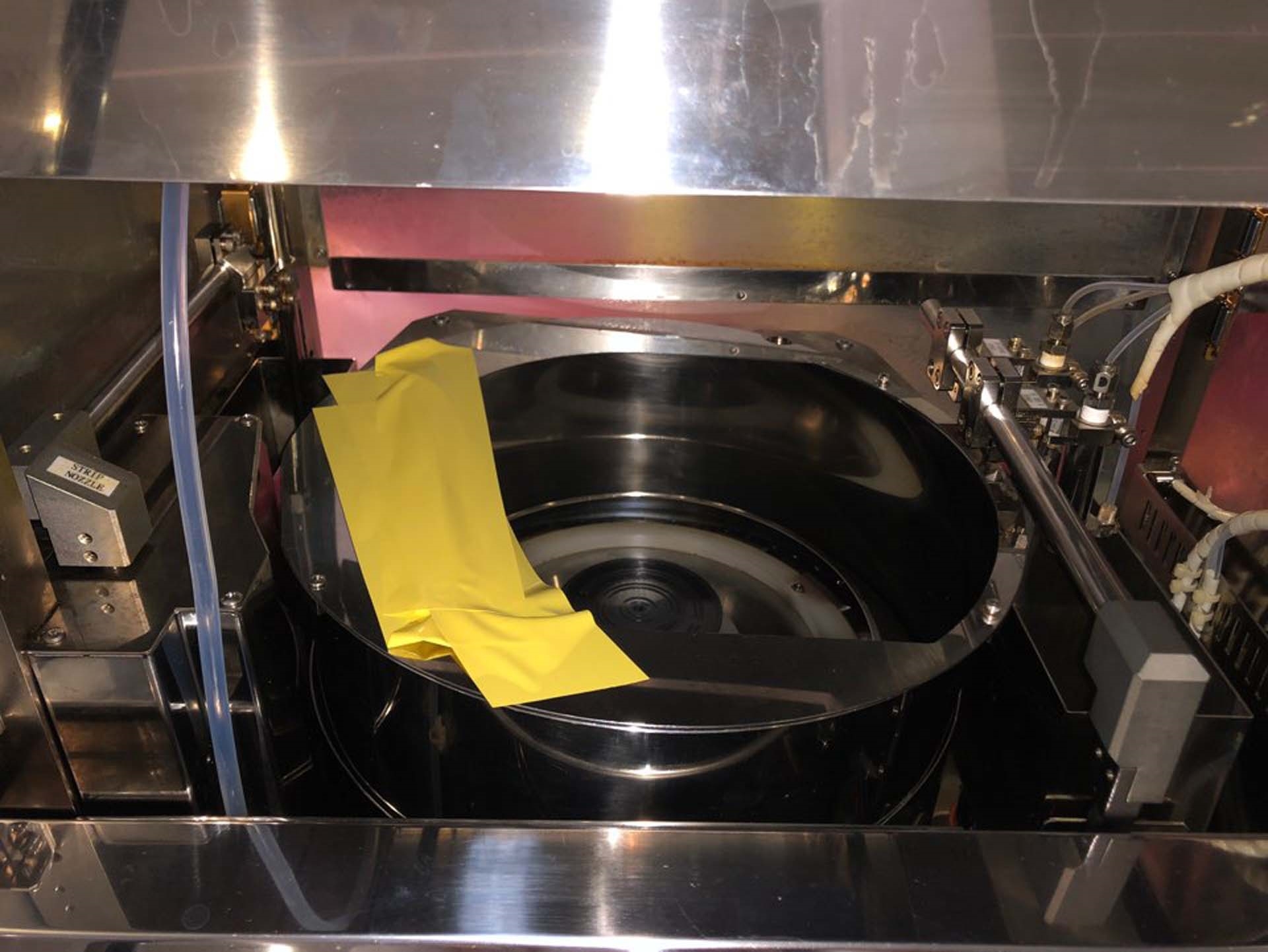


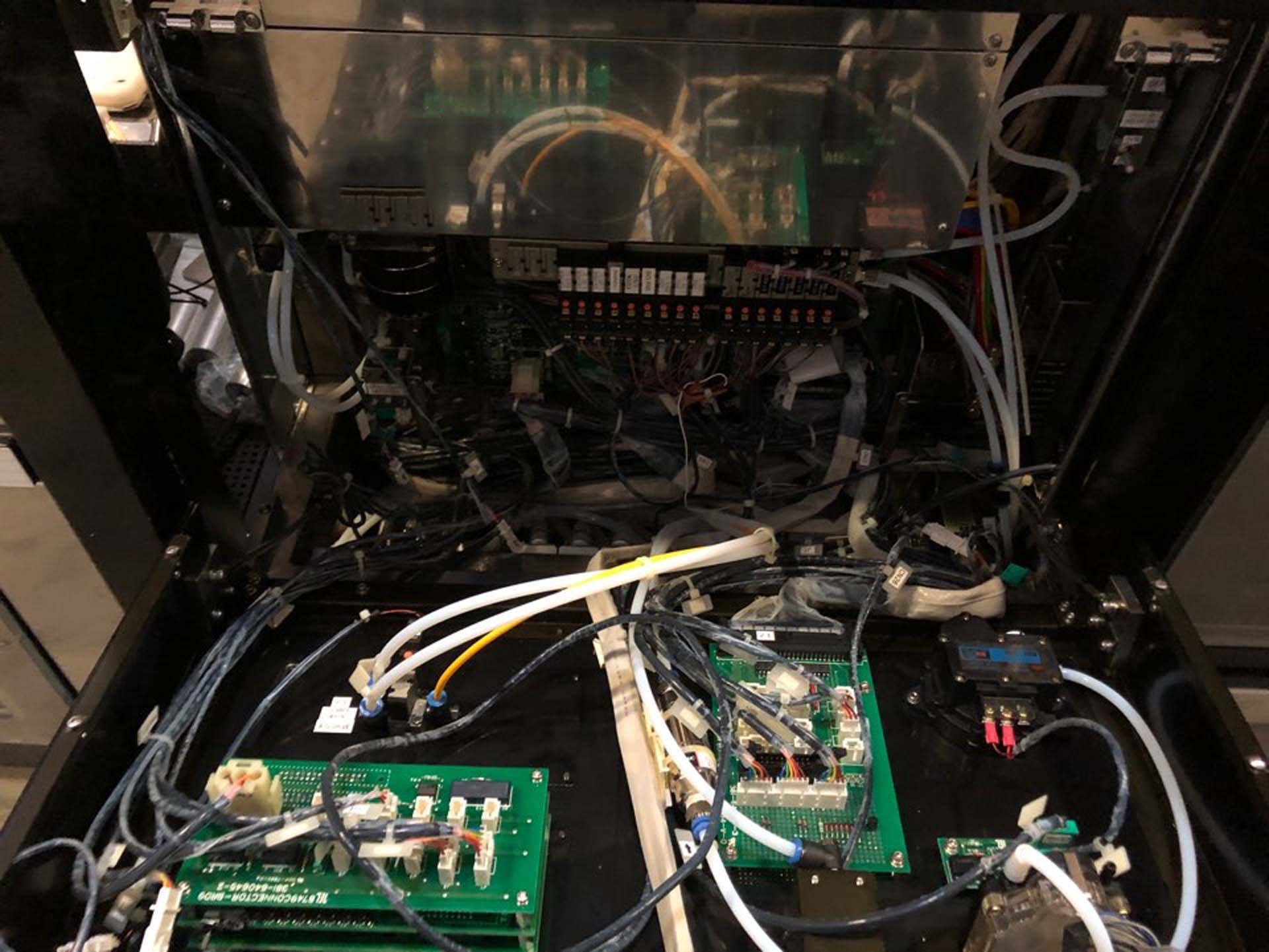

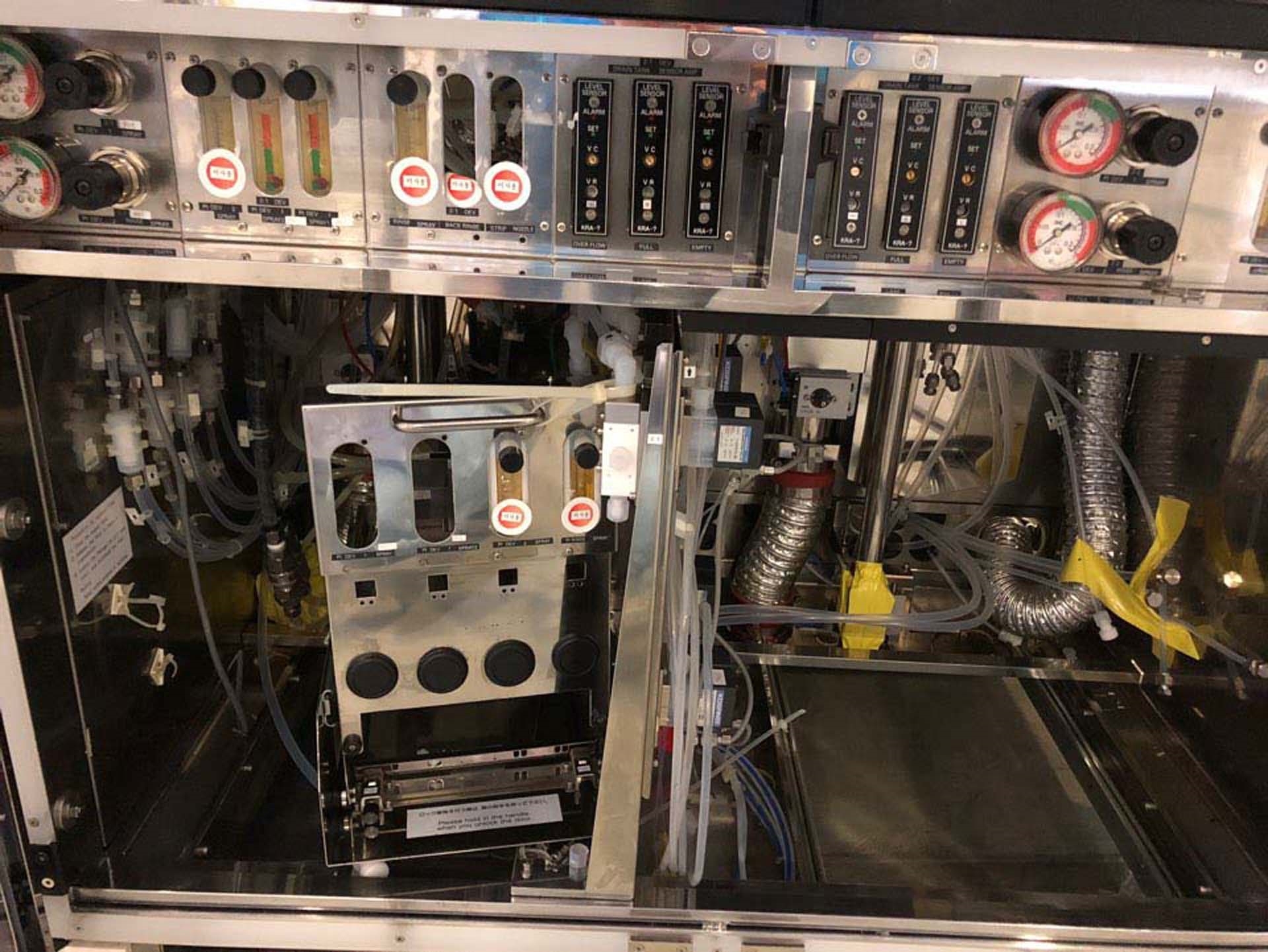


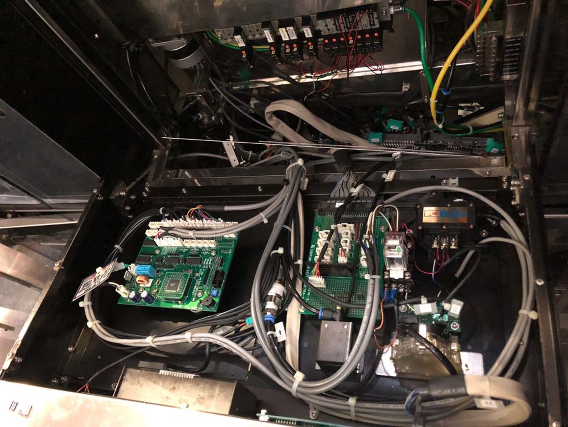


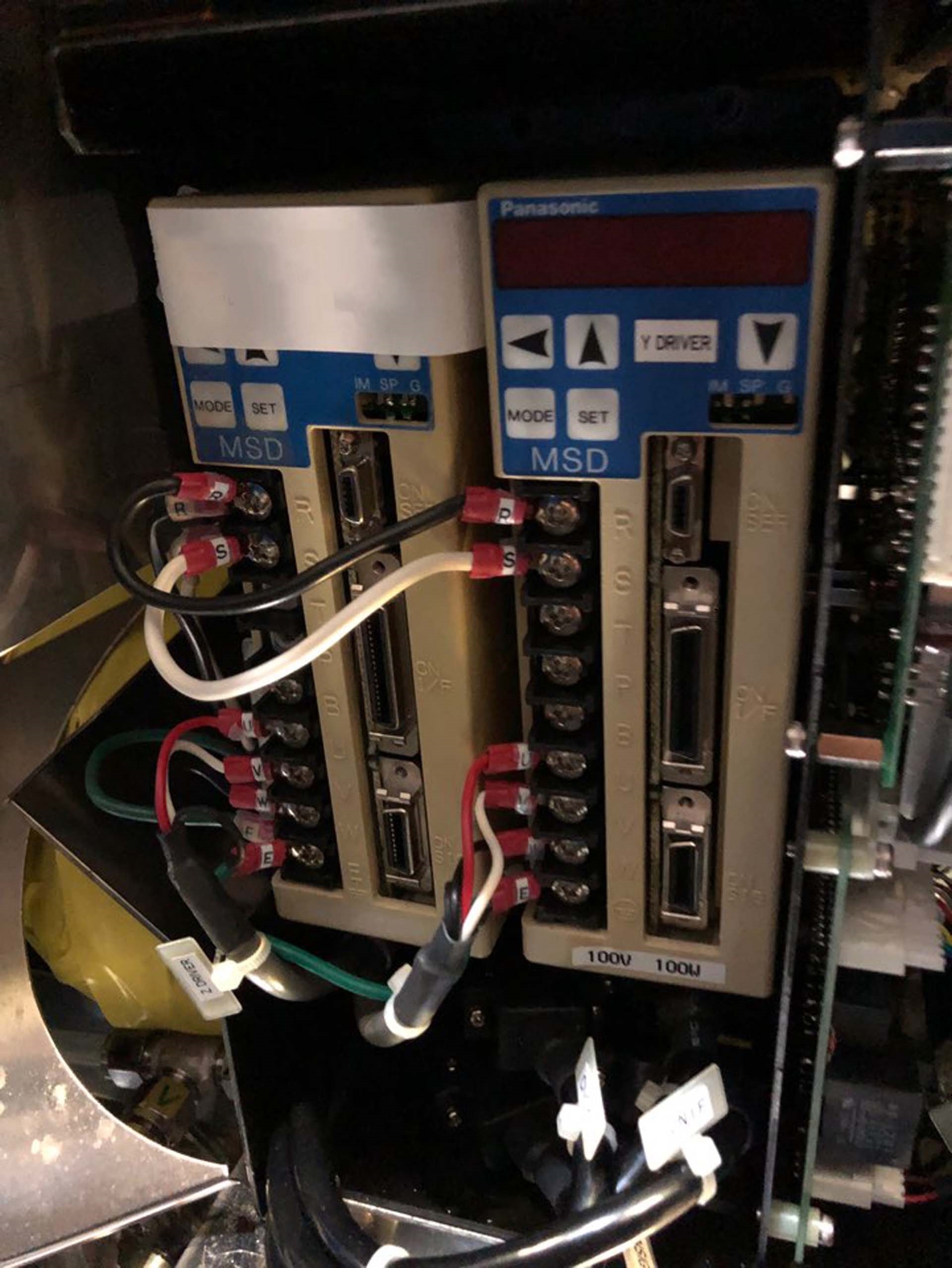

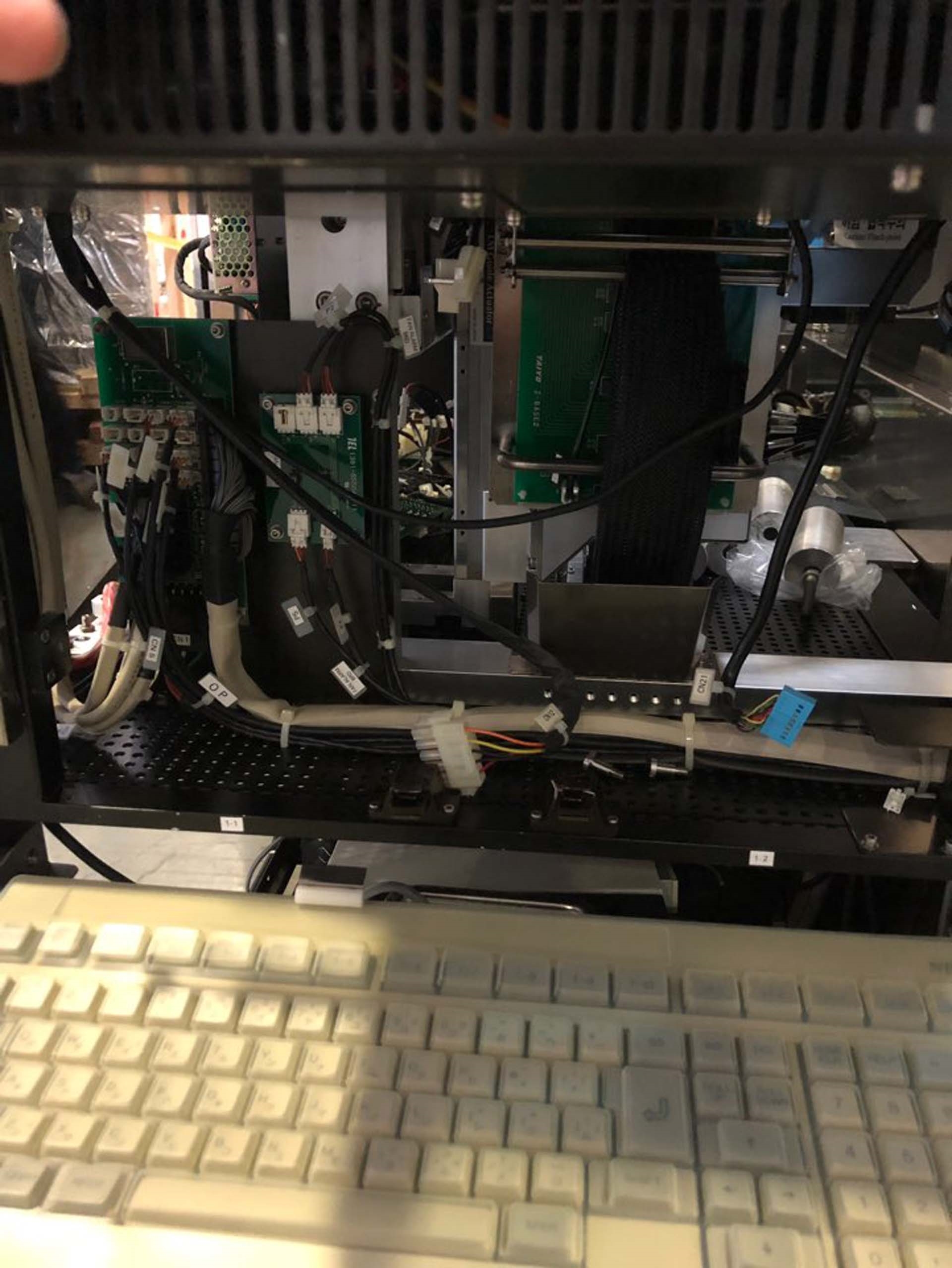

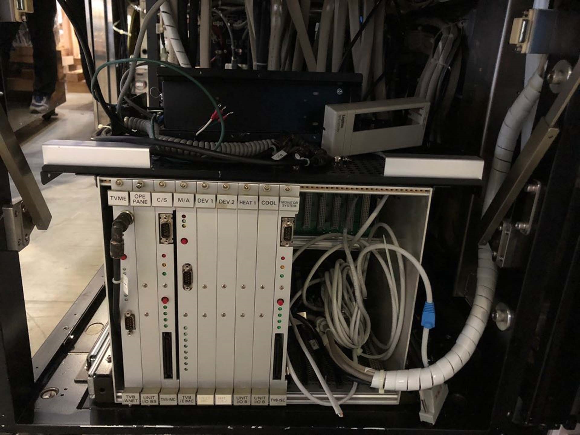

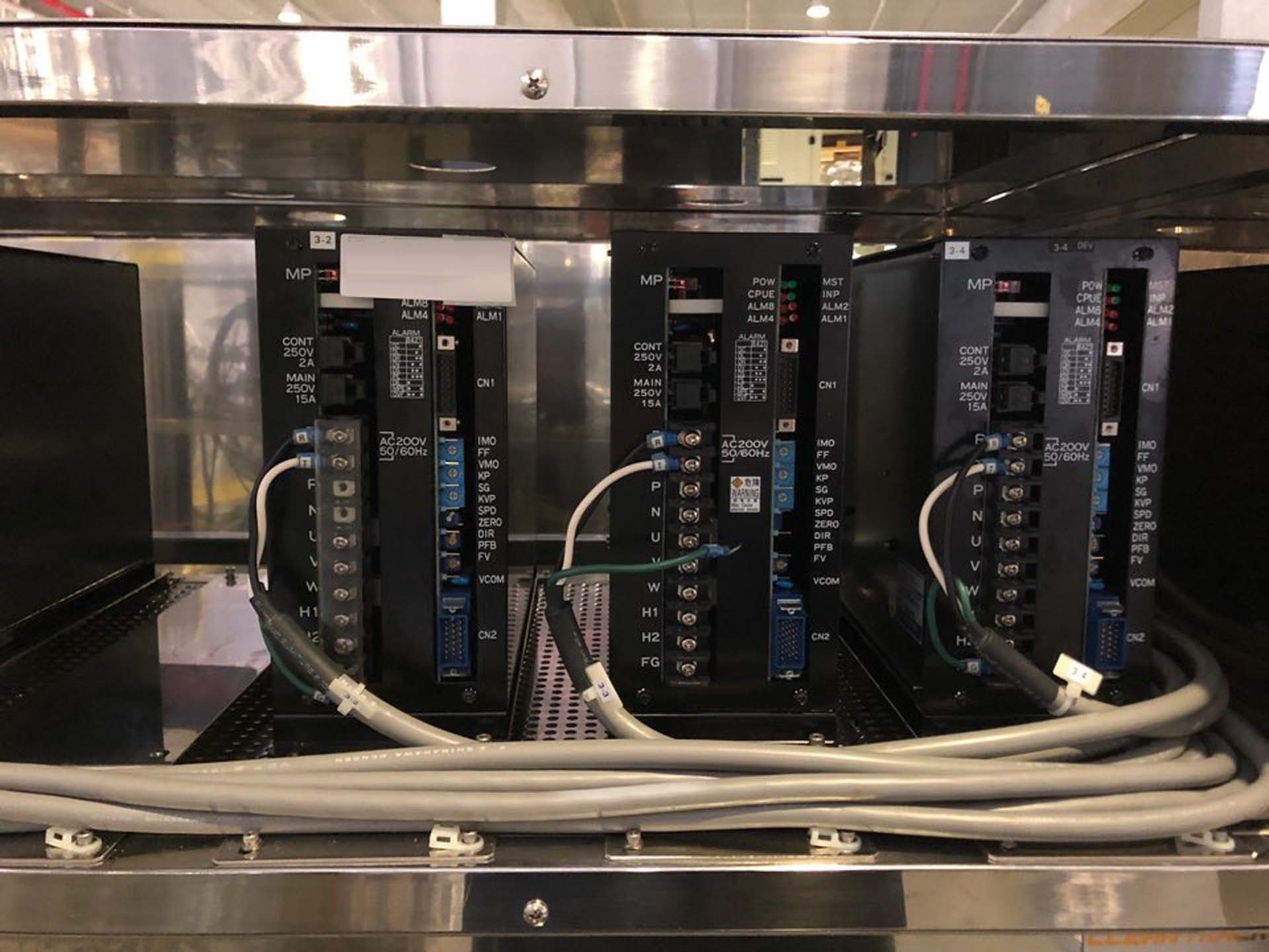


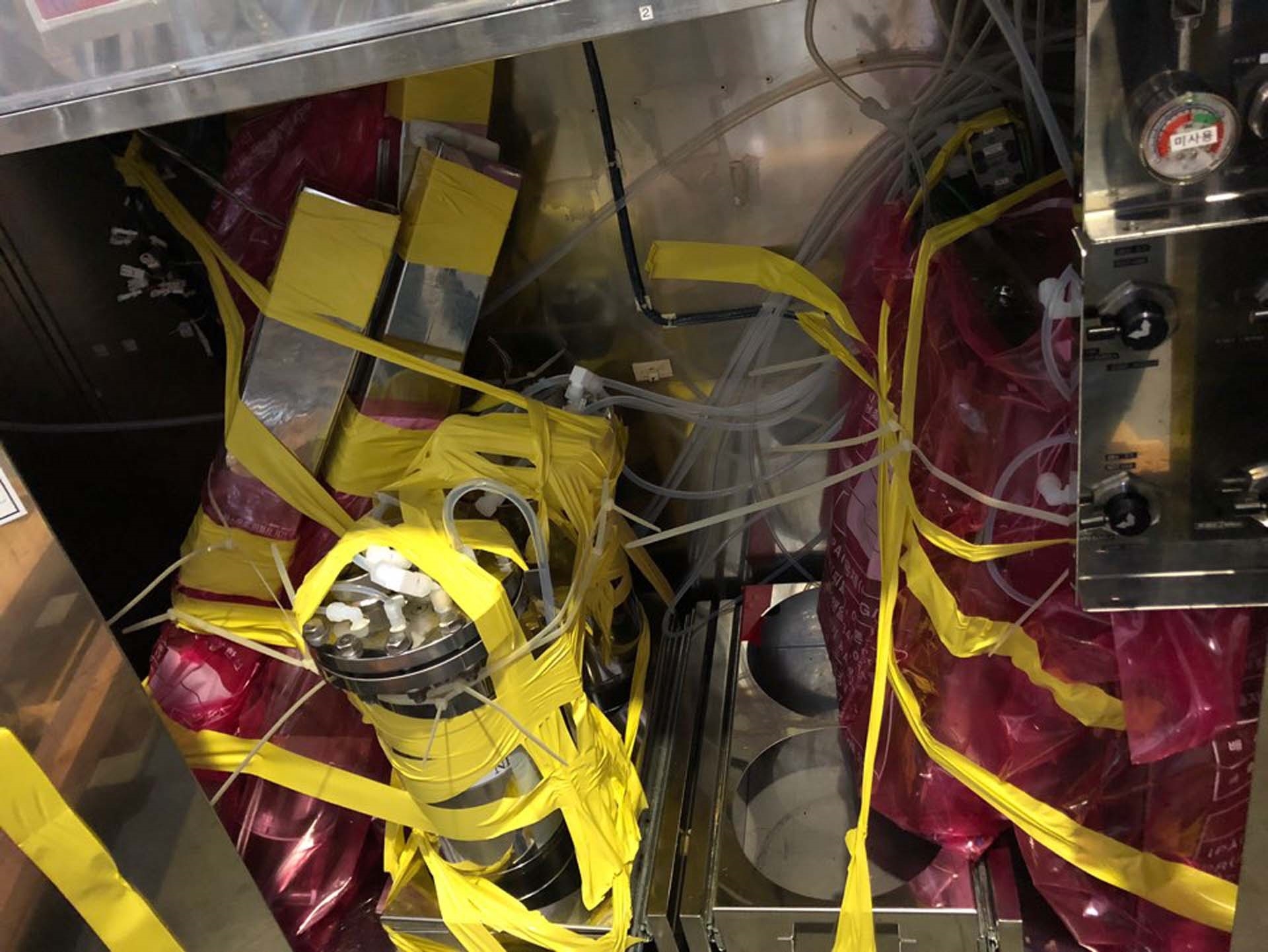

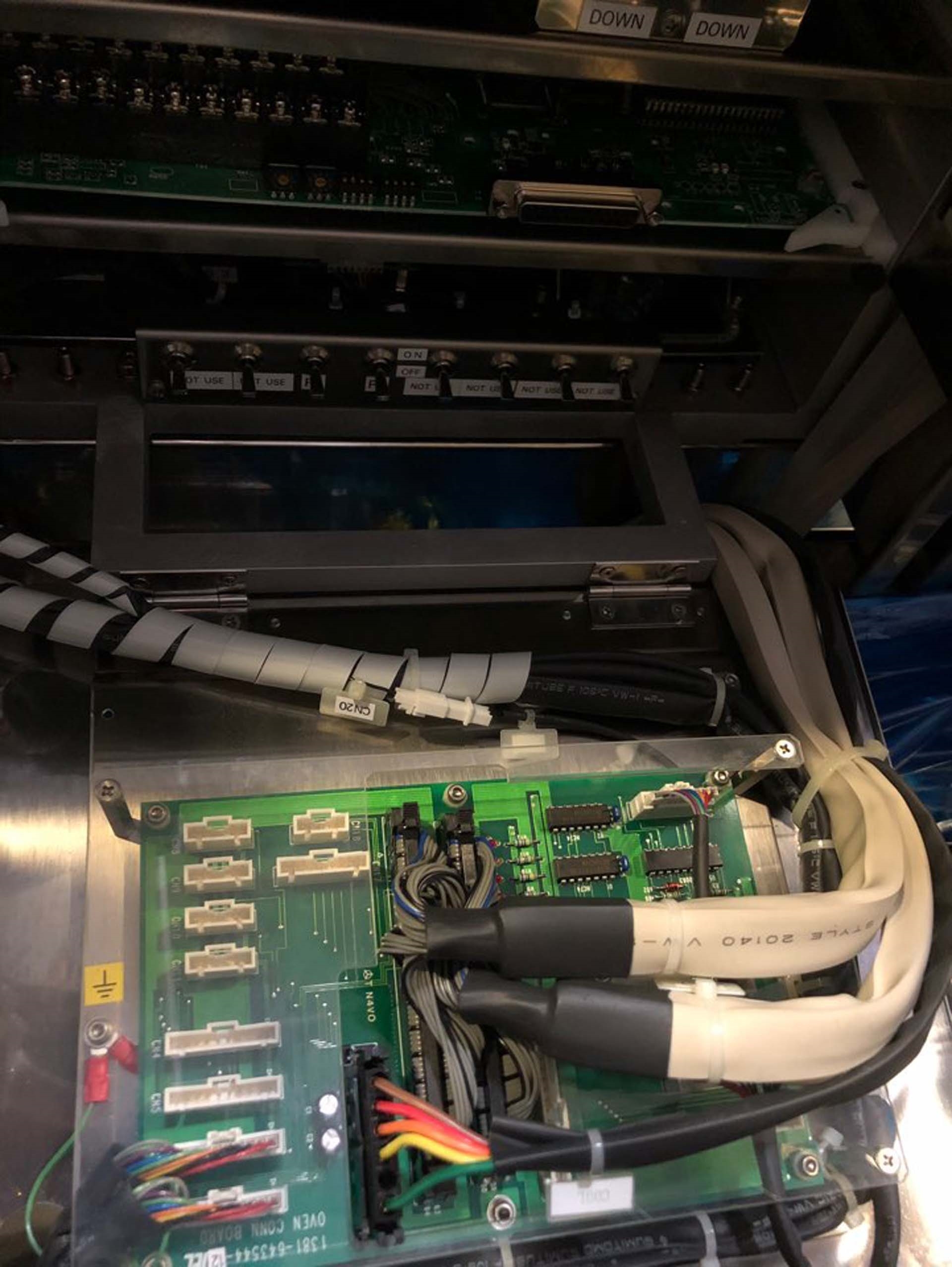




ID: 9241222
Wafer Size: 8"
Vintage: 1995
(5) Developer system, 8"
Dual block
1995 vintage.
TEL (TE) TEL / TOKYO ELECTRON Mark 7 Photoresist Equipment is a device used in semiconductor manufacturing for the deposition and patterning of thin-film layers of photoresist. It is designed to meet the advanced requirements of today's semiconductor industry and is capable of producing high-resolution images and patterns with accurate aspect ratios. The system consists of three primary components - the controller, the stable table, and the optics chamber. The controller is the main component for unit control and operation, which makes use of real-time computing, data analysis, and feedback signals to meet stringent process requirements. The stable table ensures accurate placement of a substrate during the coating and patterning processes. The optics chamber is responsible for the imaging process and features precise control of the path length and positioning of laser beams used for patterning. TEL MARK7 also features several features to enhance performance and accuracy. A low-temperature plasma activation layer is used to ensure a uniform resist layer thickness and improved adhesion of the resist to the substrate surface. The use of a high-resolution binary stepper and advanced optics chamber gives precise control of light exposure in order to create high-resolution patterns. In addition, the machine has a feature to fine tune the process to obtain the desired final pattern. Using TOKYO ELECTRON MARK-7, users can achieve precise micro-fabrication of thin-film layers with sizes as small as 0.125 micrometers. With the ability to accurately control light exposure, users can create layers with various shapes and feature sizes. The tool also supports a wide range of operational parameters, including pulse frequency, spot size, and exposure energy. This makes MARK7 a suitable asset for creating processing of complex shapes and feature sizes. TEL / TOKYO ELECTRON MARK-7 provides users with a simple and intuitive user interface, allowing for simple set-up and operation of the model. The equipment also comes with a comprehensive diagnostic and control system, which allows users to monitor each step of the process and make necessary adjustments. In conclusion, the TE TOKYO ELECTRON MARK7 Photoresist Unit provides an effective and efficient platform for the deposition and patterning of photoresist. Its combination of advanced features, advanced optics, and comprehensive machine control allows the user to produce high-resolution patterns with precise aspect ratios and feature sizes. These features make TOKYO ELECTRON Mark 7 an ideal tool for fabrication of thin-film devices and applications.
There are no reviews yet


