Used TEL / TOKYO ELECTRON Mark 7 #9352304 for sale
URL successfully copied!
Tap to zoom
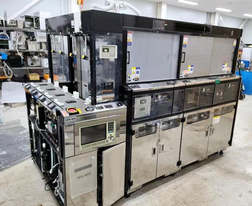


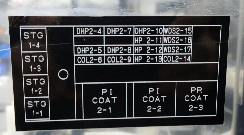

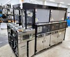
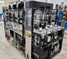
TEL / TOKYO ELECTRON Mark 7 is a scanning photoresist equipment which prepares wafers for microfabrication. This tool is essential in providing a surface layer in order to create semiconductor circuits and has become especially useful in the manufacture of modern electronic devices. TEL MARK7 system is typically used to deposit a photoresist film on a wafer. This layer of photoresist helps define the pattern required for subsequent processing steps such as photolithography, etching, and deposition. TOKYO ELECTRON MARK-7 unit employs a computer-controlled scanning slit mechanism to transfer the photoresist from a roll to the wafer surface. A light source is used to vertically illuminate the substrate and the photoresist, while the slit mechanism operates horizontally, allowing the photoresist to be deposited evenly over the entire wafer. This process can be optimized to accommodate thin layers of photoresist. MARK7 also features an integrated vision machine to provide further control as well as scanning to detect local defects. The photoresist on Mark 7 is highly accurate due to the excellent precision of the slit mechanism. This helps ensure uniformity of the required pattern on the wafer. Additionally, the tool offers high dose accuracy, with the wide slit allowing for more accurate deposition of photoresist than that achieved by a single nozzle asset. Overall, TOKYO ELECTRON Mark 7 is an effective solution for processing wafers. Its advanced technology ensures precise photoresist coverage and provides excellent thickness control. This ensures uniformity and accuracy for the production of high-quality semiconductors and electronic devices.
There are no reviews yet
