Used TEL / TOKYO ELECTRON Mark 8 #293608111 for sale
URL successfully copied!
Tap to zoom
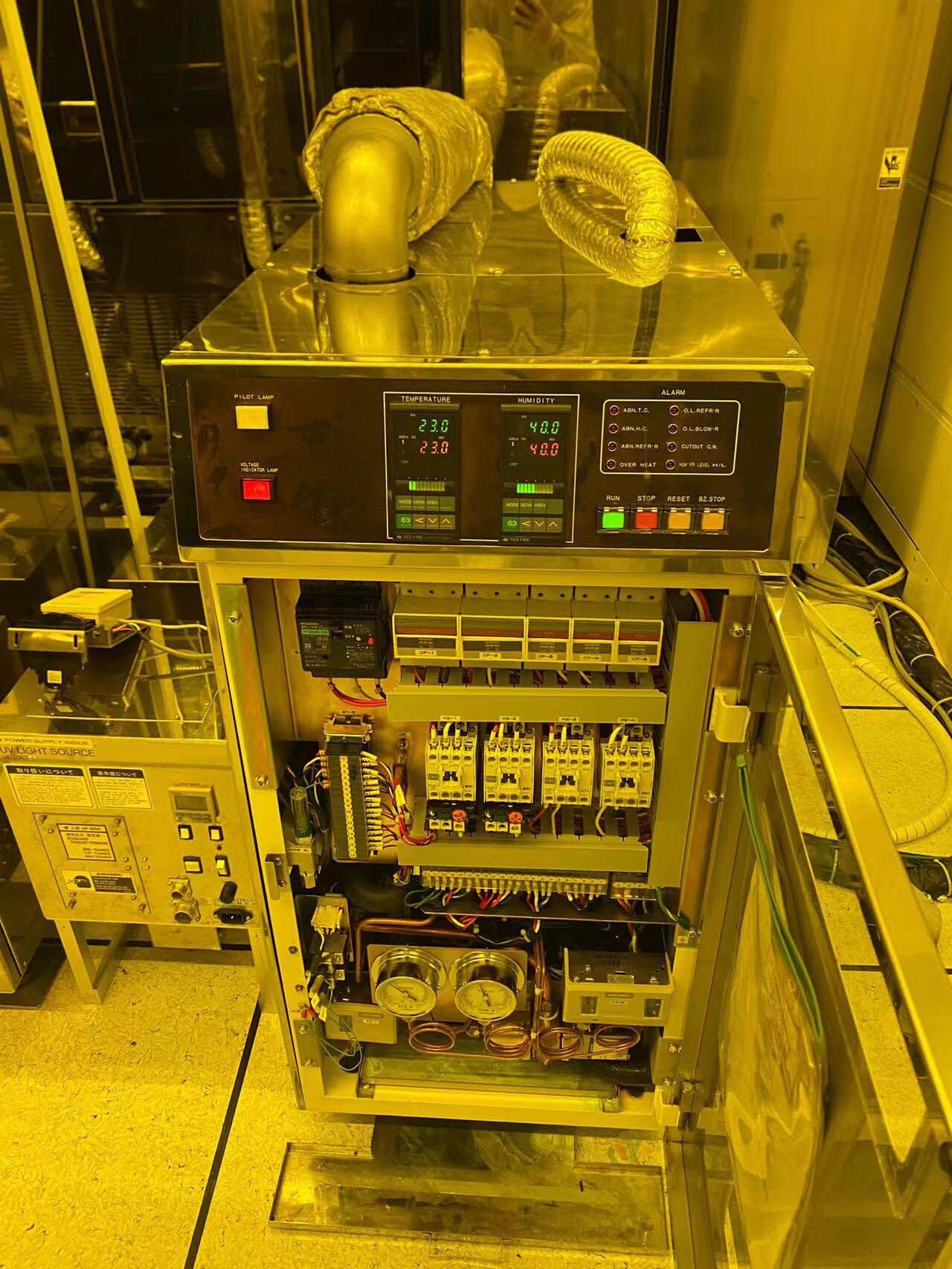


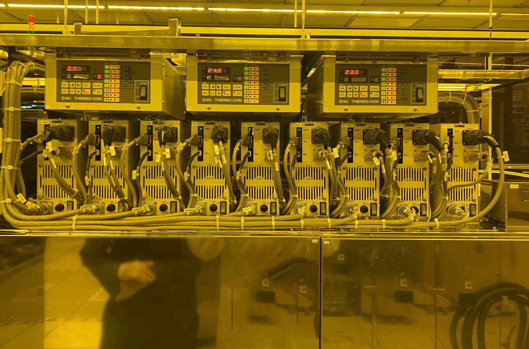

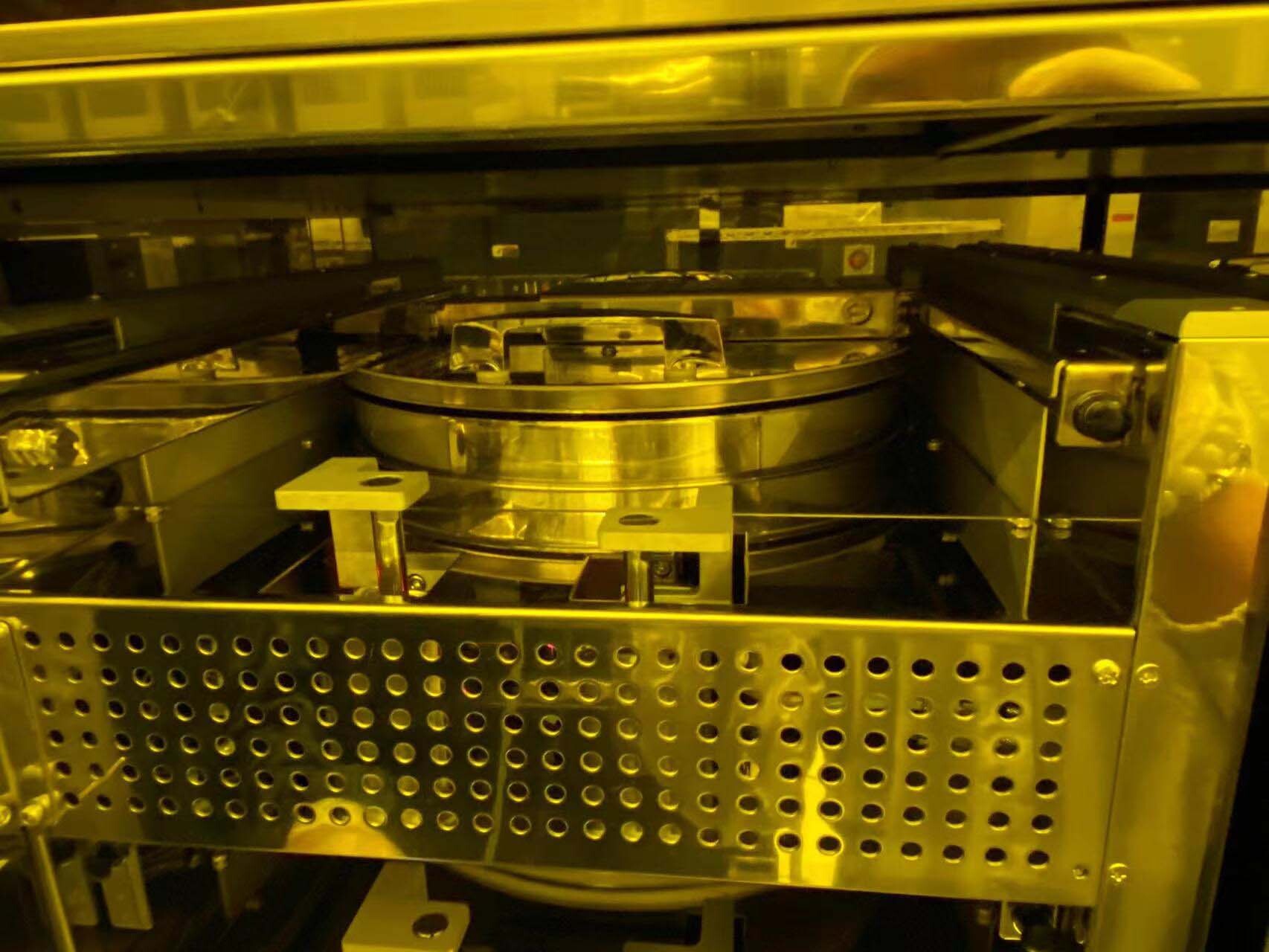

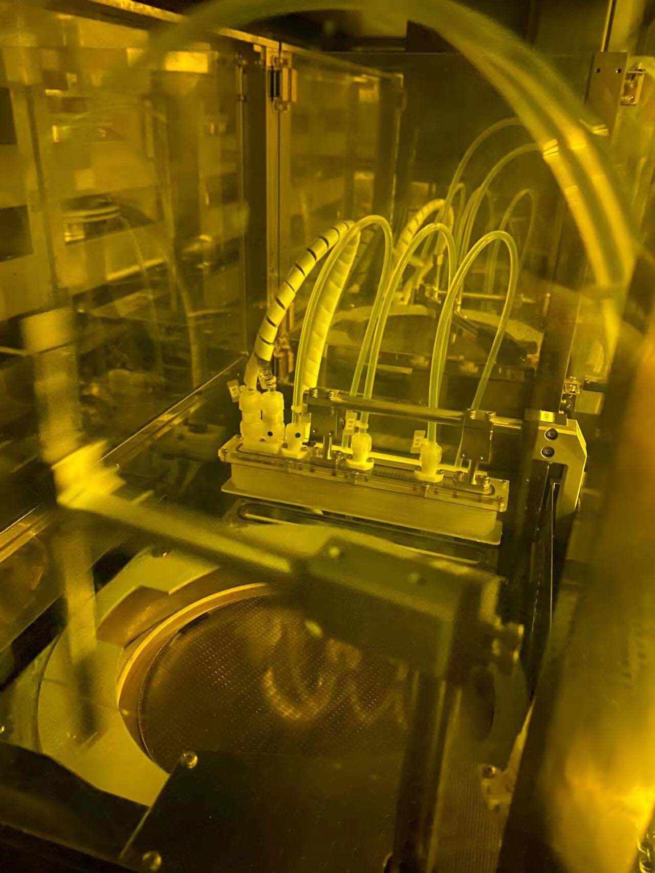

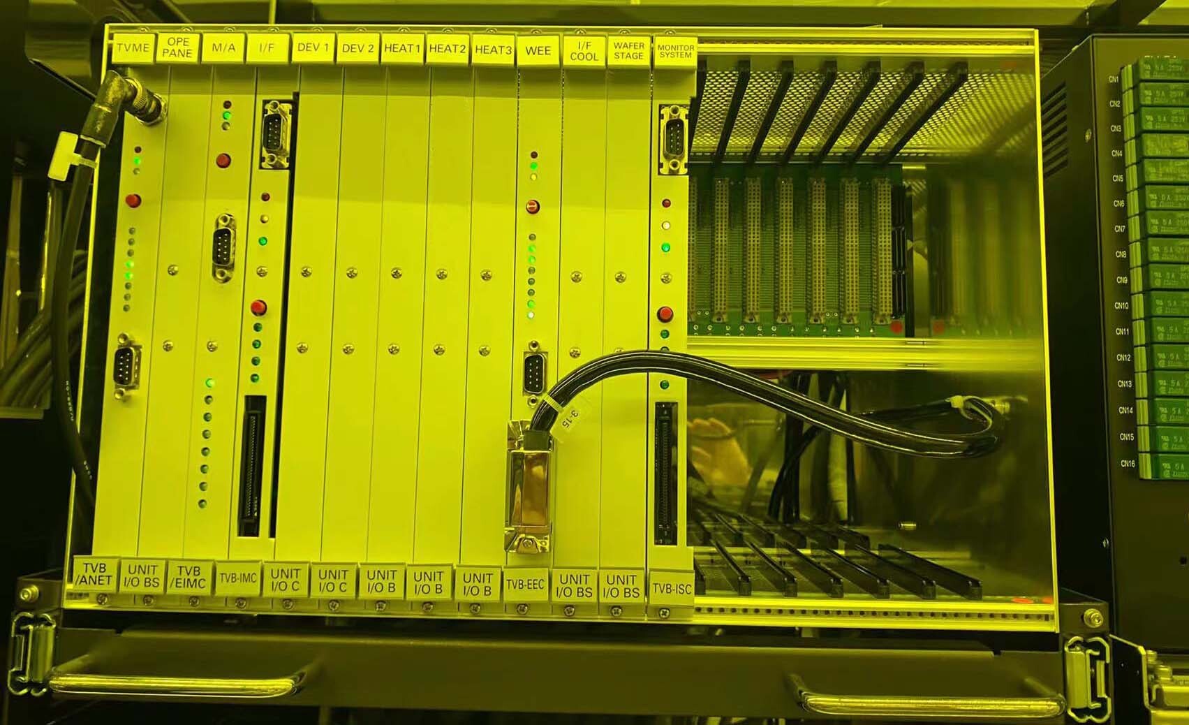

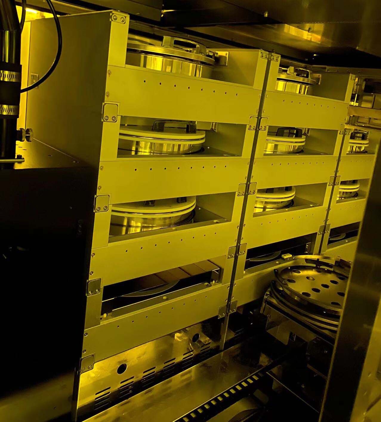

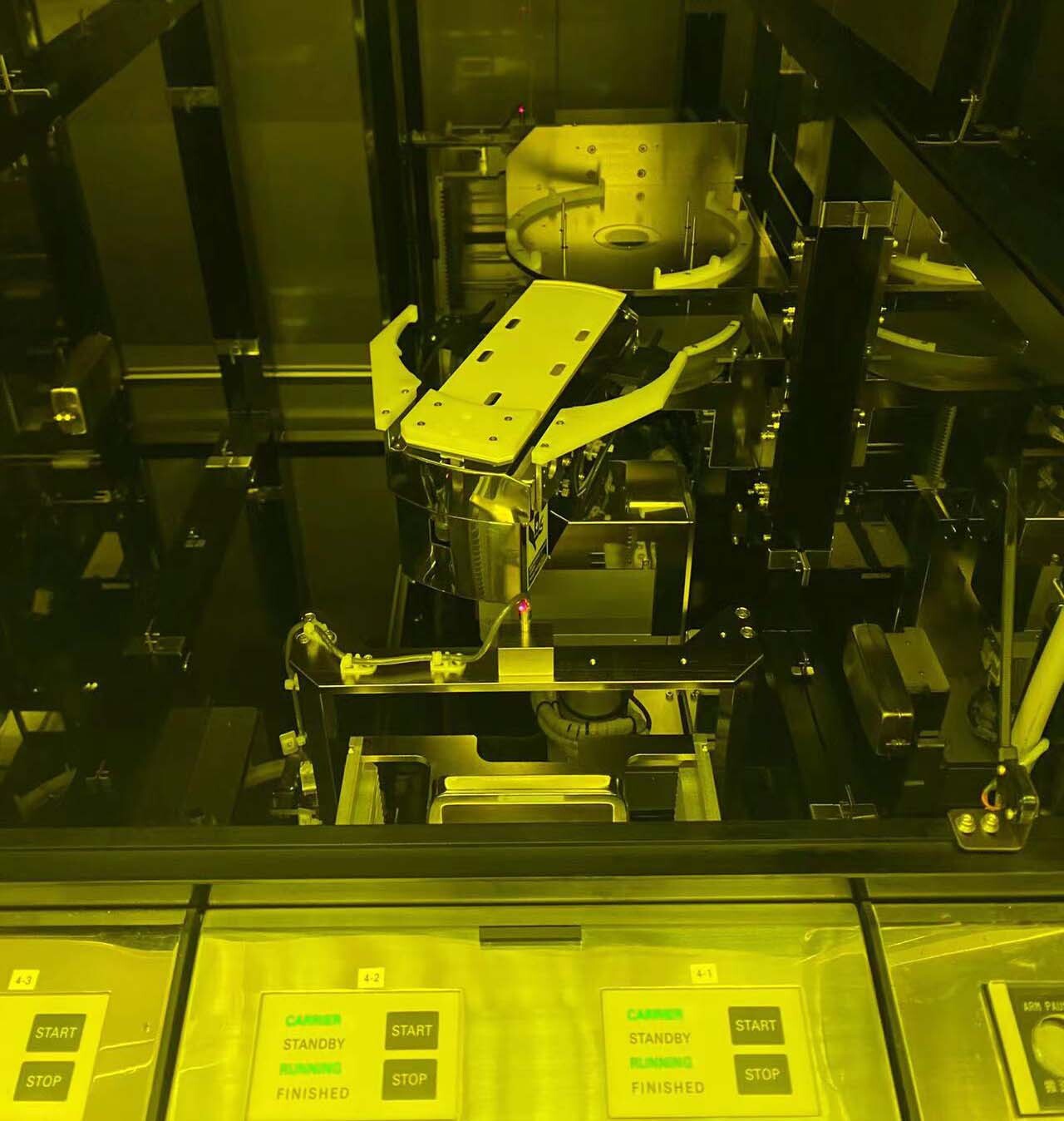

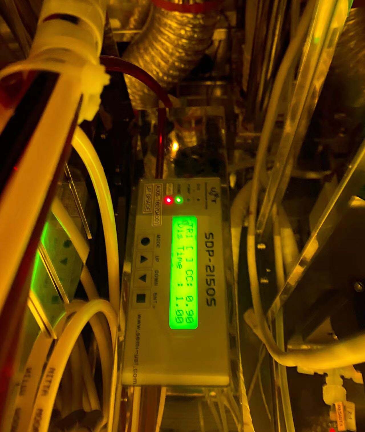

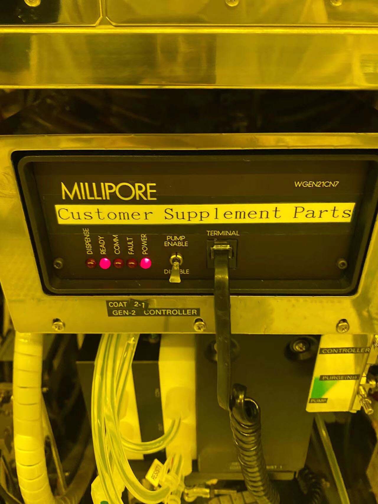


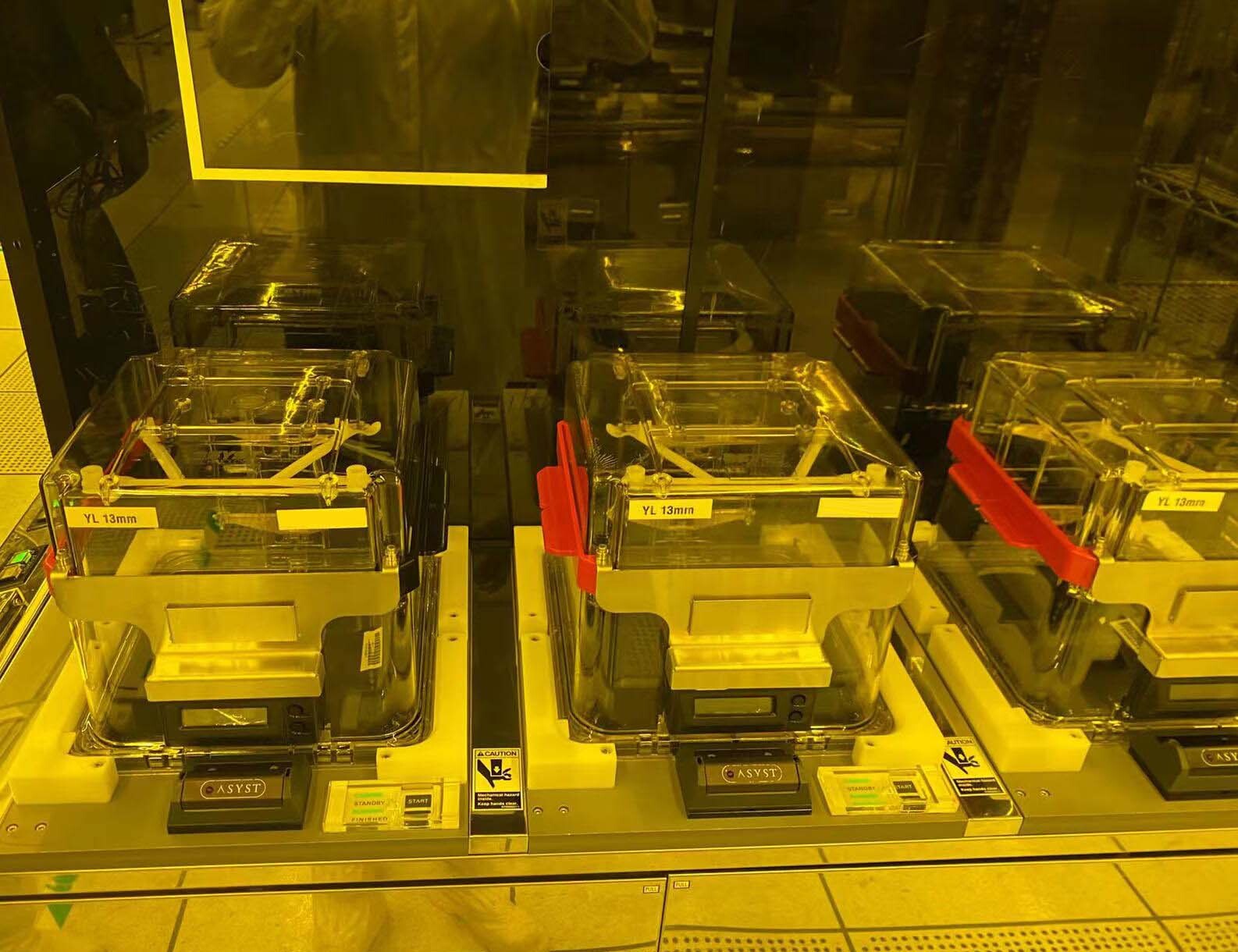

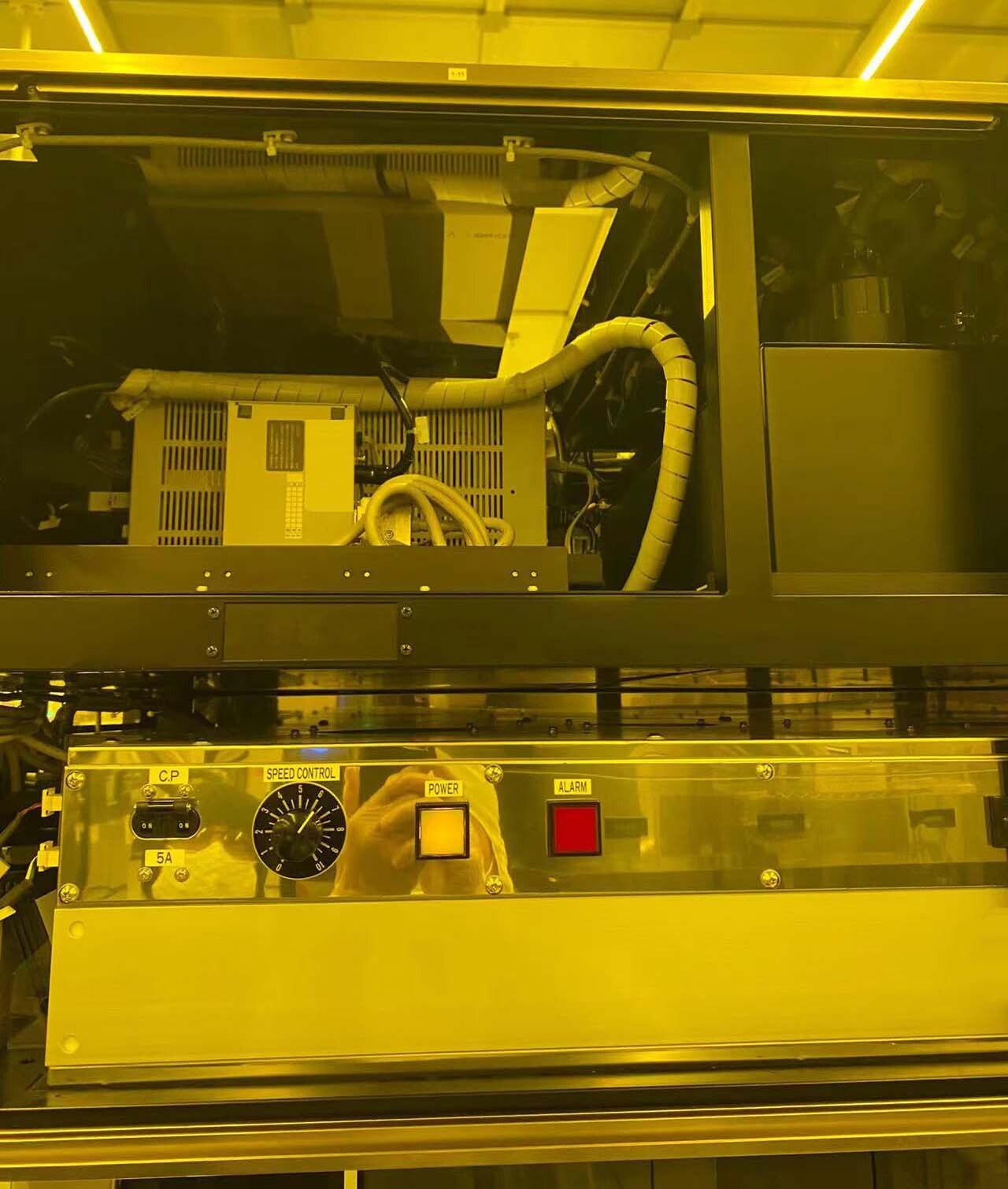

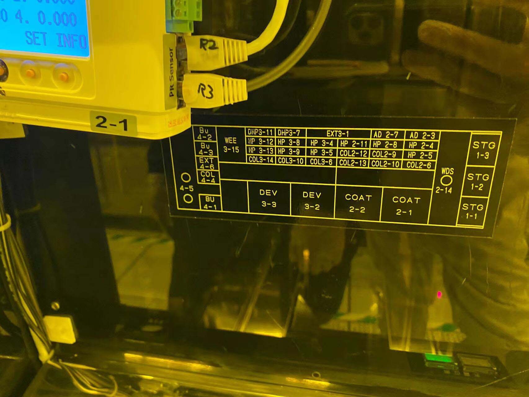

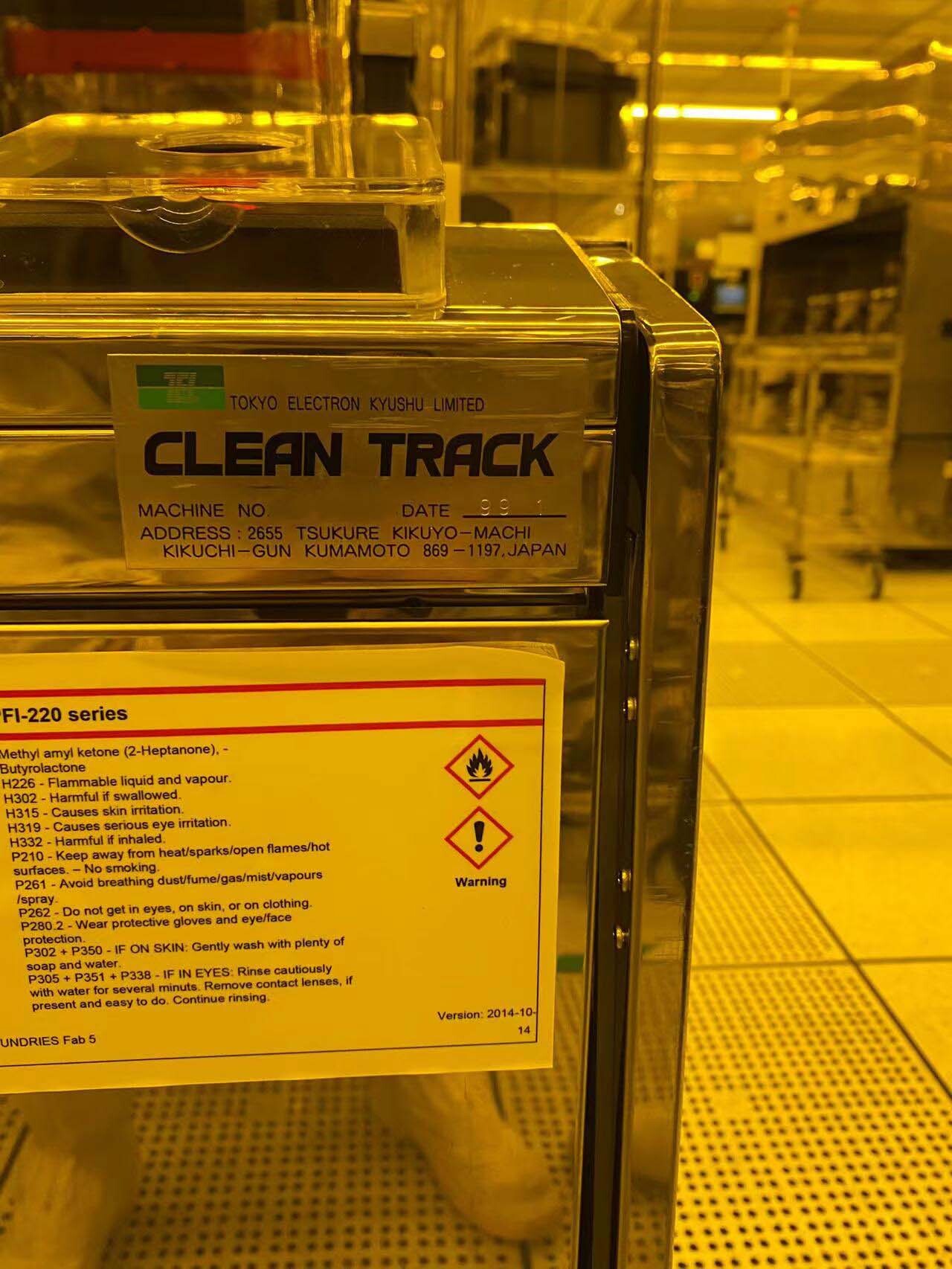

TEL (TOKYO ELECTRON) TEL / TOKYO ELECTRON Mark 8 is an advanced photoresist equipment for semiconductor fabrication. It is used for photolithographic processes such as exposing semiconductor chips or other substrates to light patterns in order to create patterns on the substrate. TEL MARK8 is capable of producing high-resolution images with up to two micron-level precision. TOKYO ELECTRON MARK-8 utilizes a computer controlled, projected imaging system which uses ultraviolet light to produce images on the substrate. This unit projects microscopic patterns of light onto the substrate, allowing exact control of where semiconductor devices will be placed on the substrate. TEL Mark 8 supports a variety of resolution levels and scan angles, allowing complete control of the images produced. TEL / TOKYO ELECTRON MARK8 is also equipped with several safety features, such as an emergency stop machine which can shut down the entire tool in case of an emergency, and an automatic shut down asset which will shut down the model automatically in case it senses an environmental condition change. This ensures a safe and secure operation of the equipment. Mark 8 also provides photoresist processing support for the creation of various types of devices. It can create applications such as the selective etching of patterns, precise pattern placement of devices, deposition of resist polymers, and through-hole filling. These capabilities, along with other advanced photoresist processing capabilities, give TOKYO ELECTRON Mark 8 the ability to produce precise images with great accuracy and repeatability. Additionally, MARK8 also supports a range of advanced image processing and analysis capabilities including image registration, alignment, recognition, and verification. These features allow TOKYO ELECTRON MARK8 to perform automated alignment and precise control when exposing a substrate with a precise pattern. This makes TEL / TOKYO ELECTRON MARK-8 ideal for the production of devices that require accurate patterns and device placement. TEL MARK-8 provides an ideal platform for quickly creating, exposing, and analyzing complex substrates. With its advanced capabilities, MARK-8 allows users to quickly create high-resolution images with precise control, accuracy, and repeatability. The system also provides a range of image processing and analysis capabilities, making it an ideal unit for semiconductor fabrication.
There are no reviews yet

