Used TEL / TOKYO ELECTRON Mark 8 #293626805 for sale
URL successfully copied!
Tap to zoom
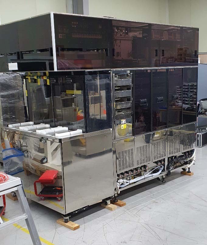


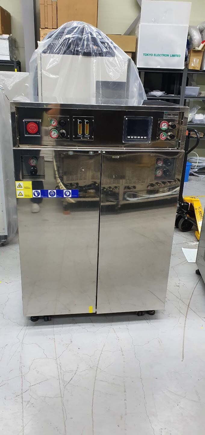

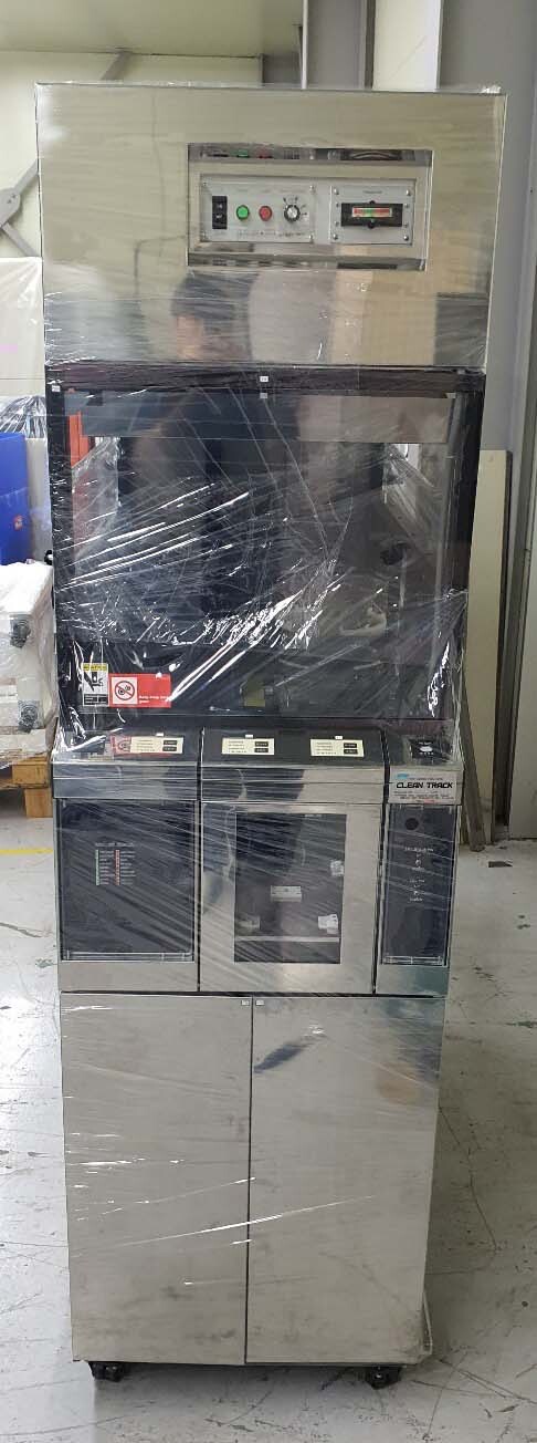

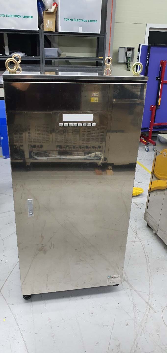


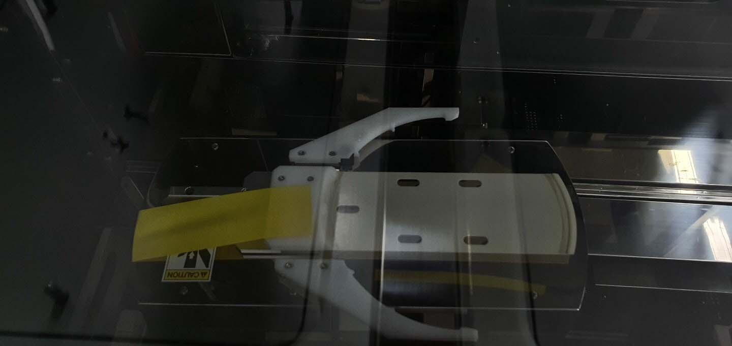

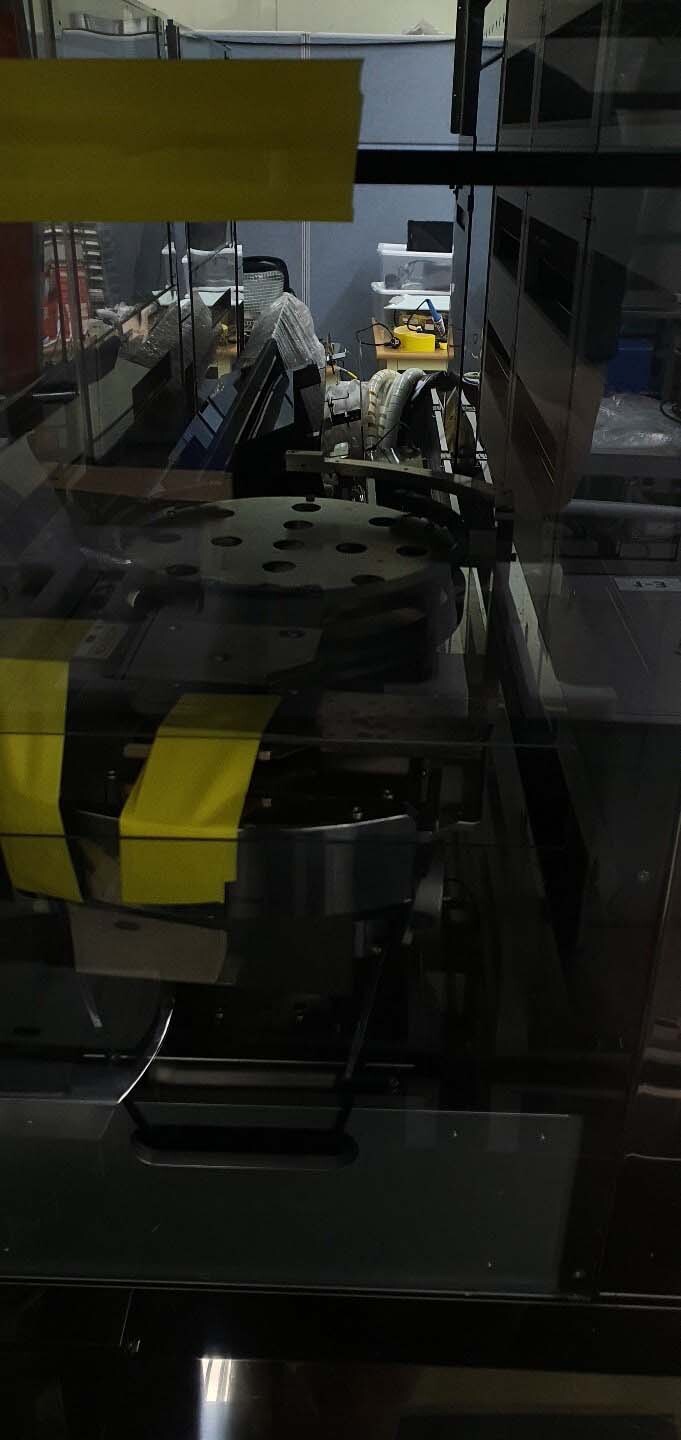

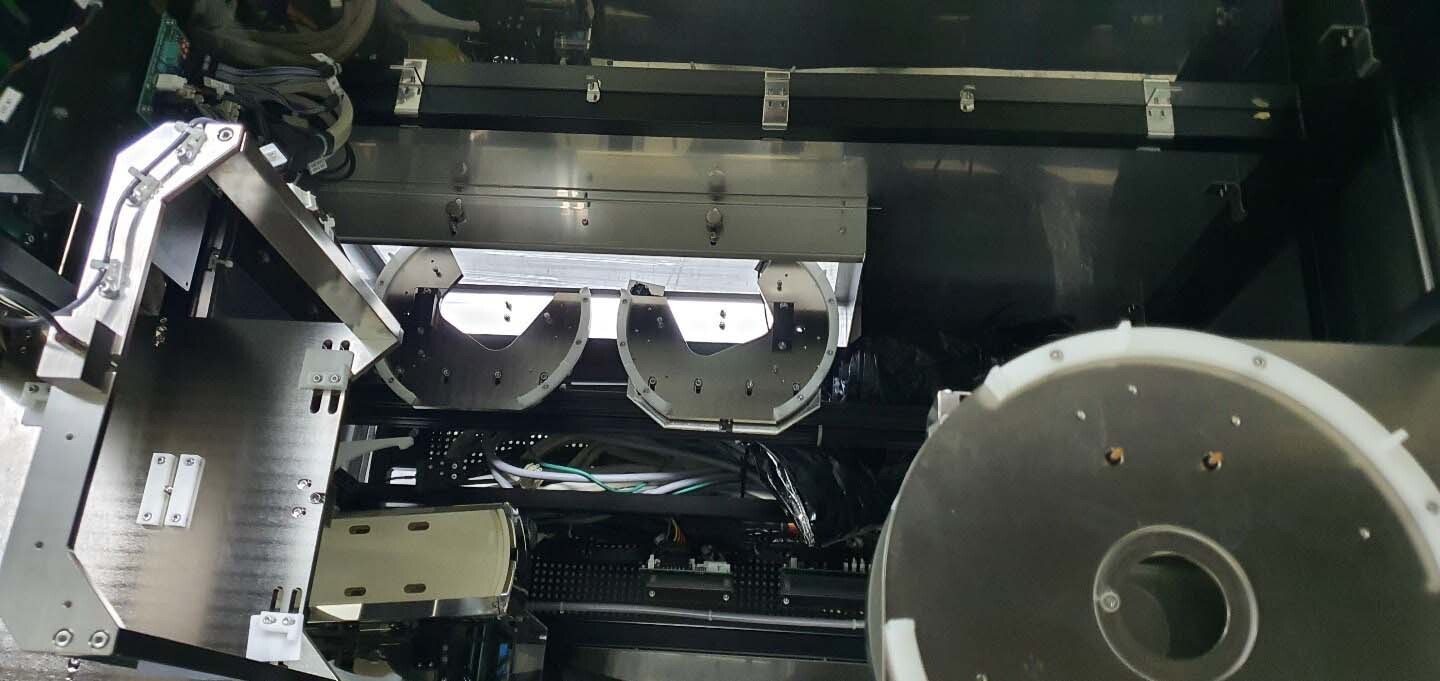

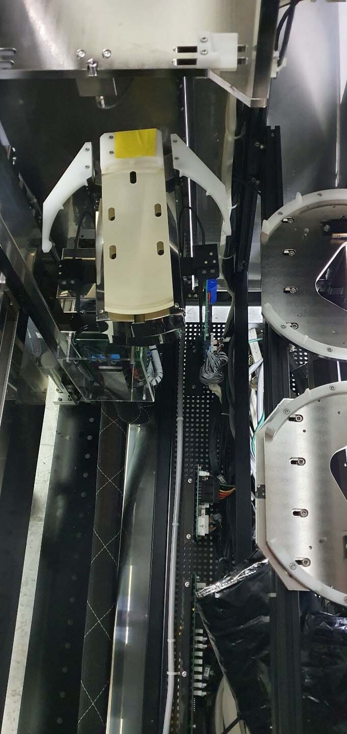

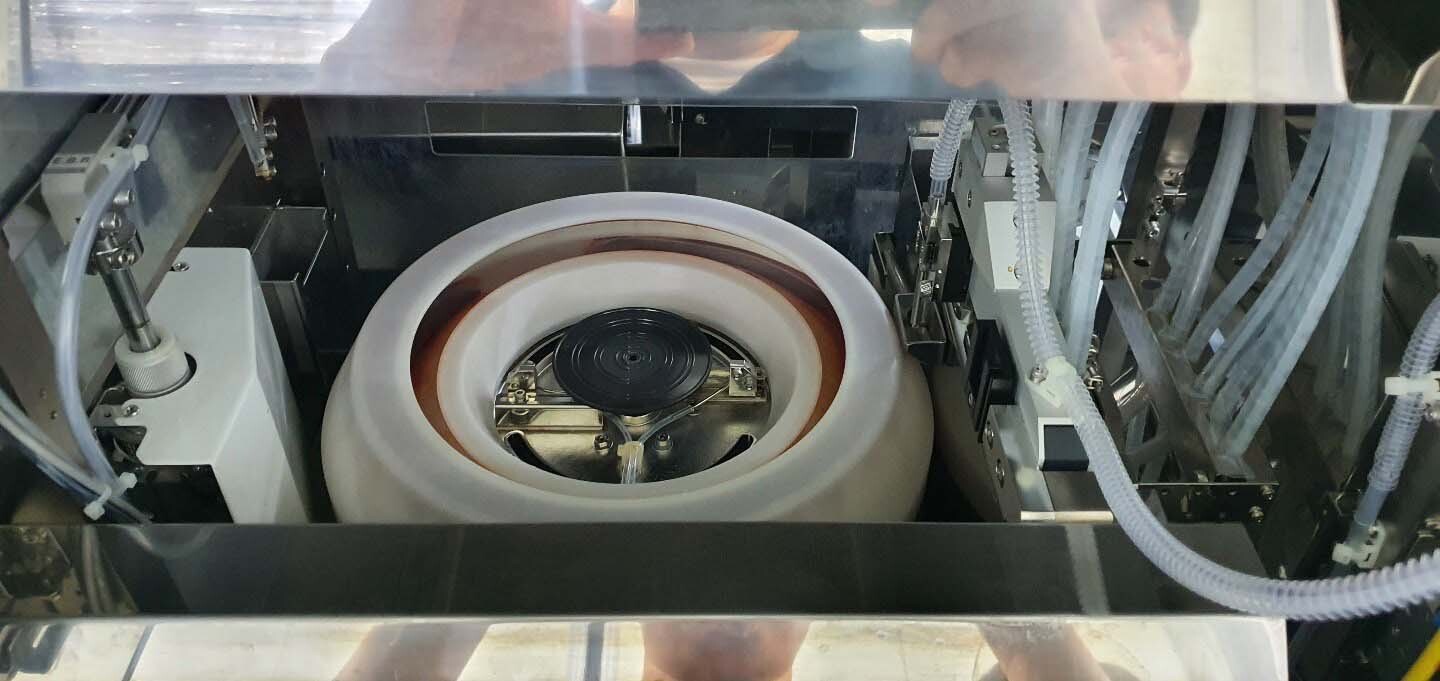

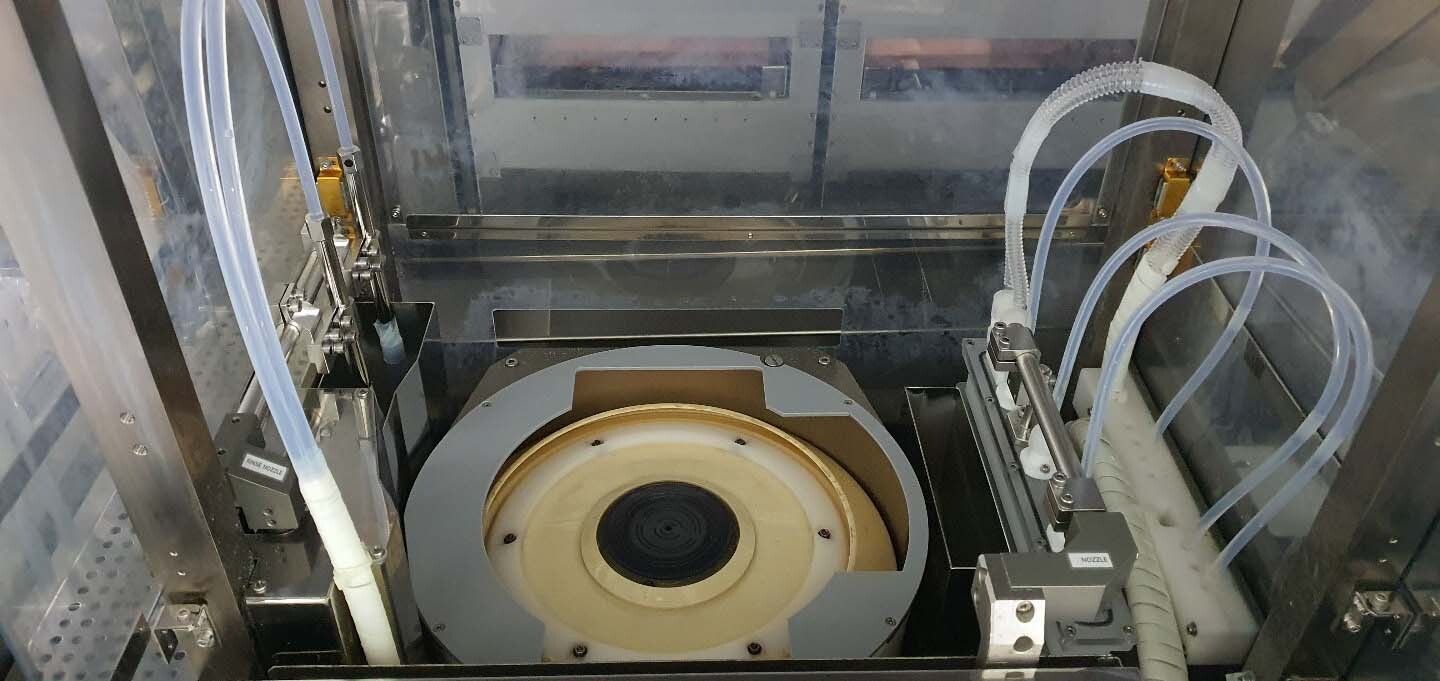


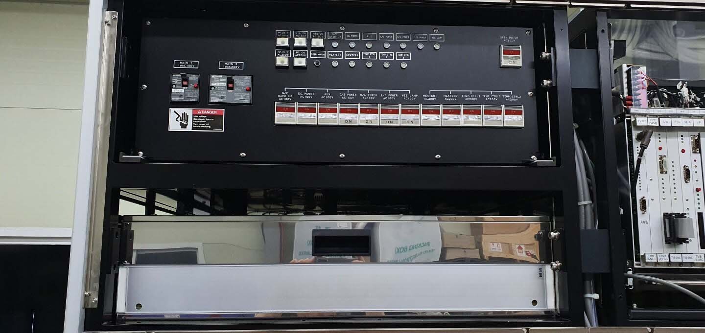

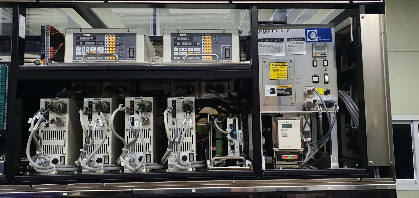

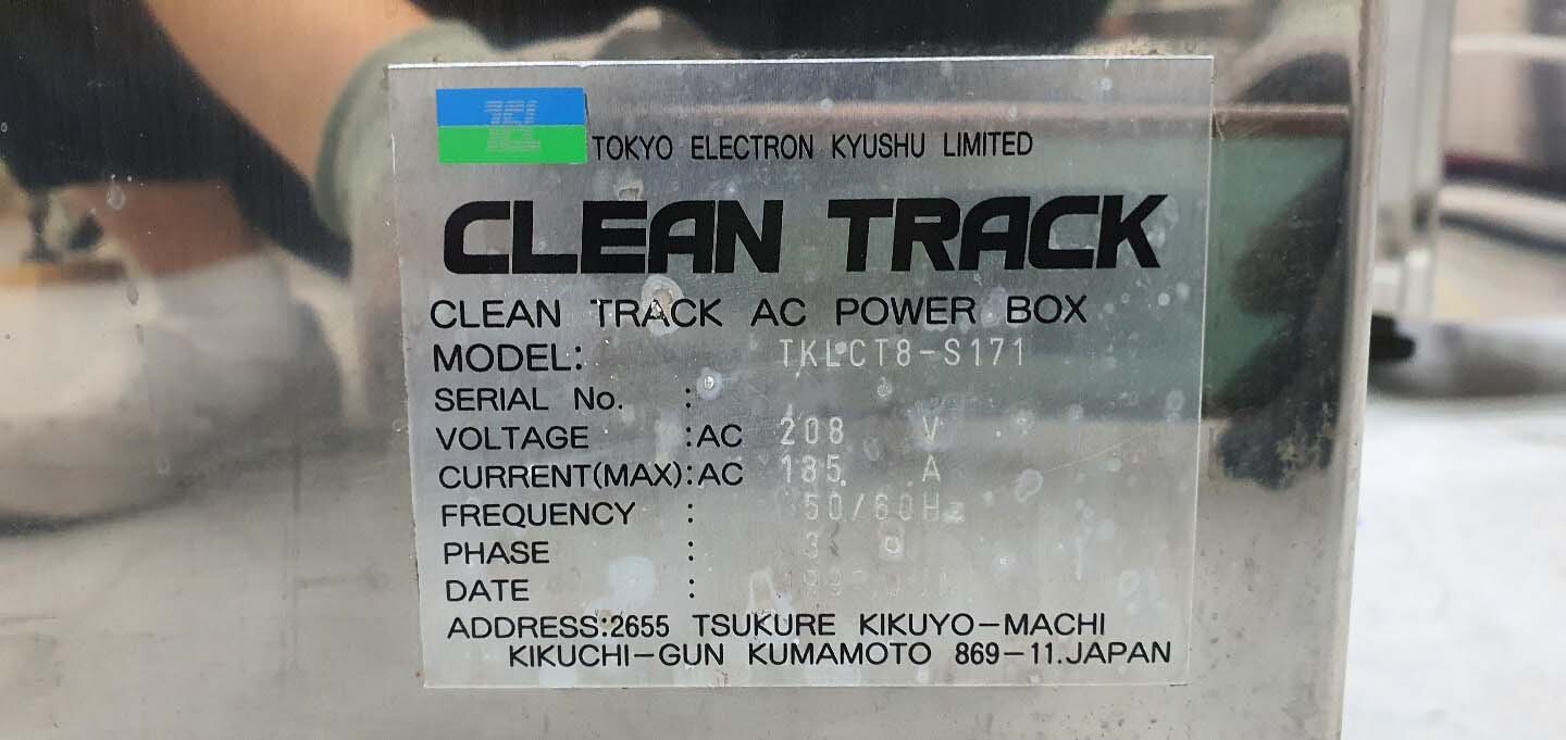

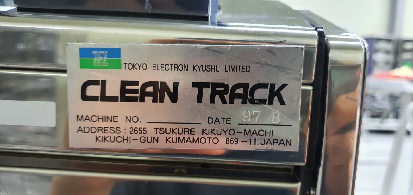

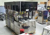
TEL / TOKYO ELECTRON Mark 8 Photoresist Equipment is a lithography system used in the production of semiconductor circuit components. It is equipped with integrated control, advanced diagnostics and monitoring, as well as an advanced automation unit to ensure accuracy and repeatability with each production. The machine has a user interface that can be used for easy manipulation of the tool parameters. The asset is designed to expose a photoresist material (particularly a photoresist film) to ultraviolet radiation, which is combined with a photomask pattern to determine the pattern on the device. This process is often used for imaging and etching the device for fine line lithography. It also has a maskless alignment model which is designed to horizontally align the wafer during exposure and increase the yield of good devices. TEL MARK8 Photoresist Equipment has a high optical resolution of 2.3 micron to 3.8 micron, which gives a high accuracy of exposing features of the photoresist film. It is also capable of patterning devices at 8x speed or faster, allowing shorter processing times. It can also support 6 inch and 8 inch wafer sizes. The system also has a particle detector to record defects or ambient conditions outside the unit. This is done to maintain its performance and extend service life of the unit. It also has special optics to minimize its outgassing, preventing contamination of the film during exposure. TOKYO ELECTRON MARK-8 Photoresist Machine also has a specially designed auto-focus tool which is used to auto-adjust the focus length of the lens for better performance. It also has an auto-dose mechanism which automatically adjusts the dose of radiation for each layer of the substrate. This ensures that the right amount of energy is applied to the substrate at each layer. In addition, TOKYO ELECTRON Mark 8 Photoresist Asset has a highly accurate wafer stage and advanced software tools that provide repeatable and reliable performance. This ensures that the production results are consistent and repeatable, providing a greater level of reliability for critical processes that make semiconductor devices. Overall, Mark 8 Photoresist Model is the ideal tool for lithographic processes in the semiconductor industry, providing exceptional accuracy and repeatability for production lines.
There are no reviews yet

