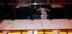
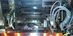
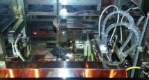
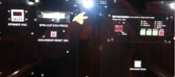
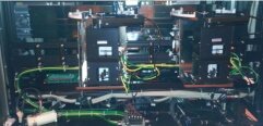
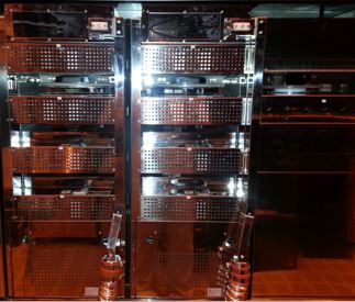
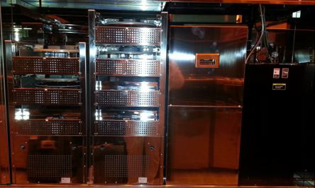
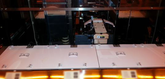
Used TEL / TOKYO ELECTRON Mark 8 #9155211 for sale
URL successfully copied!
Tap to zoom





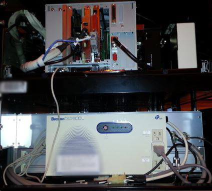


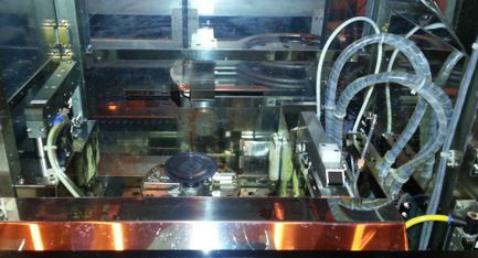

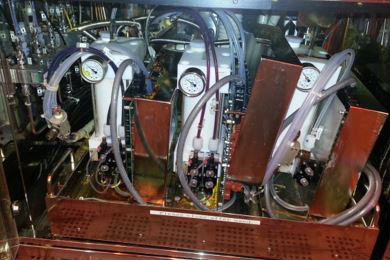

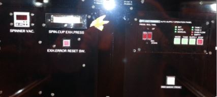


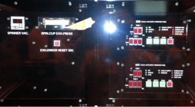


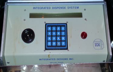


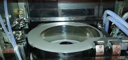


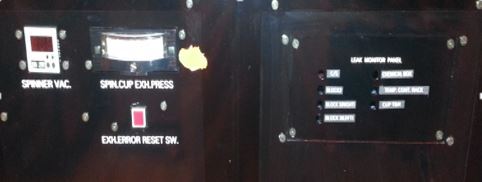











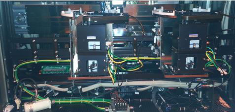

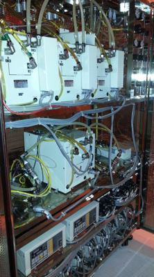

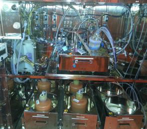

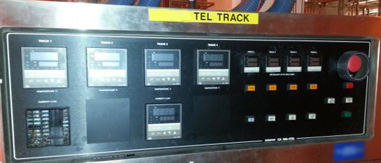

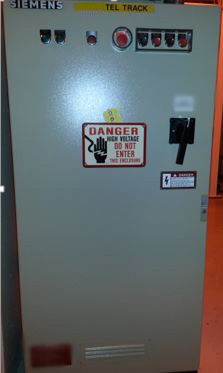


ID: 9155211
Wafer Size: 8"
Vintage: 1995
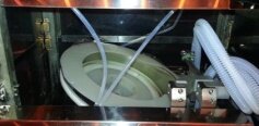
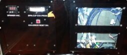
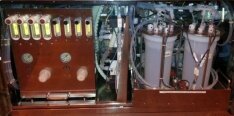
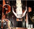
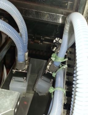
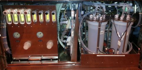
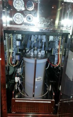
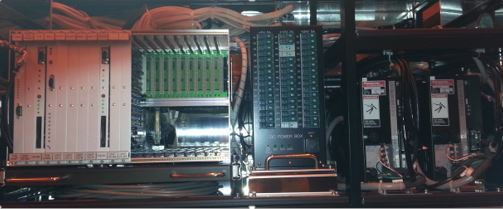
Wafer coater, 8"
Carrier station type: Open cassette
Wafer loading type: Right to Left
Software version: MK8H2.78(MC) M8B9083D.00 (Block)
Coater unit:
Pump model: RRC
Nozzle count: 3
Development unit:
Dev nozzle: H-Nozzle
Dev nozzle Count: 2
Up/Down move: Cylinder
Rinse nozzle: Stream
1995 vintage.
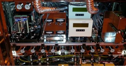
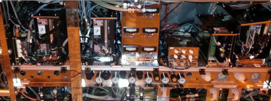
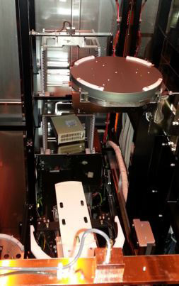
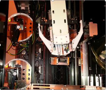
TEL / TOKYO ELECTRON Mark 8 Photoresist Equipment is an advanced lithography system designed for photoresist deposition and processing. It uses an advanced mask projection technology that enables the projection of a microstructured photoresist film onto a pattern on a silicon wafer. This makes it ideal for applications such as MEMS, optical, and microfluidic devices. The unit consists of a substrate stage, mask projection machine, and resist coating tool. The substrate stage is used to hold the substrate in place and is capable of controlling the substrate's temperature and humidity. The mask projection asset is the main component of the model and it consists of a laser projector, alignment optics, and optical cleaning and maintenance equipment. The laser projector utilizes a 327 nm laser line and is capable of projecting a high-resolution pattern onto the substrate. The alignment optics are used to align the laser beam to the mask field and the optics provide a high-level of precision for the photoresist pattern. The optical cleaning and maintenance system helps to remove contamination during deposition. The resist coating unit is used to apply the photoresist material onto the substrate. The machine utilizes a high-pressure spray tool that applies a thin uniform layer of photoresist to the surface of the substrate. The spray asset is equipped with multiple nozzles and a computer-controlled program to ensure the photoresist is deposited uniformly and accurately. TEL MARK8 Photoresist Model has a guaranteed 15-year lifetime accuracy of 0.1μm and provides reliable and accurate results. It is suitable for high-precision photoresist deposition applications. It has been widely used in the industry for applications such as 3D printing, MEMS, optical, and microfluidic devices.
There are no reviews yet

