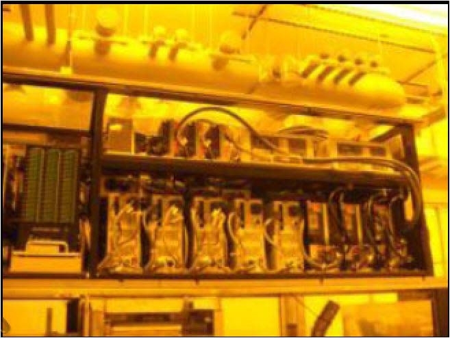
Used TEL / TOKYO ELECTRON Mark 8 #9190379 for sale
It looks like this item has already been sold. Check similar products below or contact us and our experienced team will find it for you.
Tap to zoom


Sold
ID: 9190379
Wafer Size: 8"
Vintage: 1997
(3) Coaters / (2) Developers system, 8"
Flow: Right to left
Dual block
Type: Standard
System:
AC Cable length: 10 m
Signal cable length: 8 m
Tubing length: 8 m
EMO Signal logic: Normal close
Signal tower: (3) Colors (Red, green, yellow)
Coater:
Filter (Resist, solvent) status: ENTEGRIS
Pump type/status: 2-1 Coater R1, R2
Drain pipe connector type (PR Line): 1" (SUS)
Developer:
Developer dispense piping/tubing status:
3-2: 1/4" (Stream)
3-3: 1/4" (Spray)
DI Water dispense piping/tubing status: 3-2, 3-3: 1/4" (Stream)
Filter(DI,DEV) status: ENTEGRIS
Drain pipe connector type: PVC(¢ 32 x 25)
In-line with stepper/Scanner type: NSR
Thermo controller type: SMC (INR-244-112B)
Chemical box:
Solvent supply: Local
Developer supply: Local
EXH supply:
GEN
(12) SOL
Facility:
Power supply: AC 100/200 V, 60/75 A, 50/60 Hz, 1 Phase
1997 vintage.
TEL / TOKYO ELECTRON Mark 8 is an advanced photoresist processing equipment developed by TEL. It is designed to provide efficient and precise control throughout photolithography processes in the microelectronics industry. TEL MARK8 offers automated wafer transfer mechanisms, high-quality exposure and development functions, as well as a large selection of post-exposure processes. TOKYO ELECTRON MARK-8's advanced semi-automatic loading system allows for fast and accurate changing of lenses and features the capability to supplement precision during exposure. Its advanced wafer loading unit features a specific wafer geometry and enables maximum chip coverage along with a low-bend profile during loading and unloading. MARK8's cutting-edge exposure machine provides key accuracy and precision for photolithography processes. Through high-accuracy and high-precision LSI stepper systems, the tool is capable of exposing patterns that require submicron resolutions with a high-performance laser onto photoresist. This allows for accurate patterns to be exposed on wafers. Overall, TEL Mark 8's exposure asset is highly efficient and allows for more production throughput and less downtime. TEL MARK-8 also offers an advanced post-exposure treatment model, which includes pas use processes, such as etching, baking, ashing, and confirming. The equipment is able to automate a wide range of post-exposure processes, allowing for repeated use and fine-tuning for a range of customer needs. This ultimately allows for higher quality and precise results with shorter cycle times. MARK-8 is built to provide maximum repeatability while ensuring a high degree of accuracy. The system's key functions, including the exposure and post-exposure treatments, are designed to work in harmony, providing the best possible results without sacrificing safety. Overall, Mark 8 is a highly advanced and efficient photoresist processing unit. It provides fast, accurate exposures, automated wafer transfer capabilities, and post-exposure treatment machine, allowing for high-quality results with fewer cycle times. This makes it an excellent choice for microelectronics and semiconductor fabrication.
There are no reviews yet