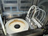
Used TEL / TOKYO ELECTRON Mark 8 #9215817 for sale
URL successfully copied!
Tap to zoom


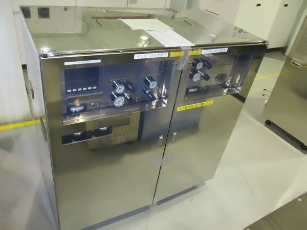

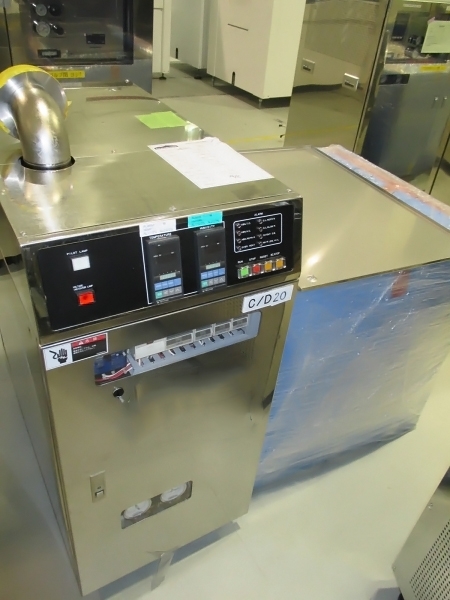

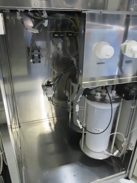

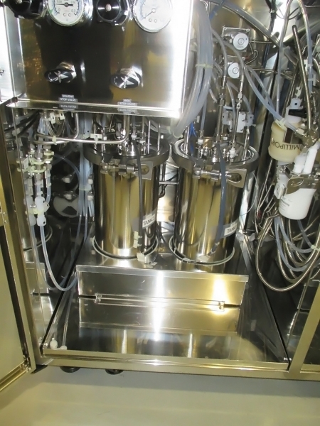

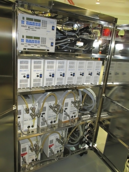

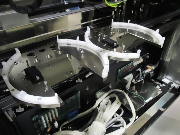


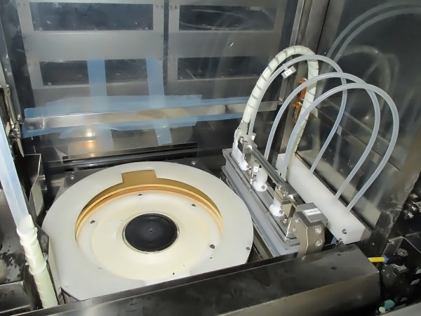

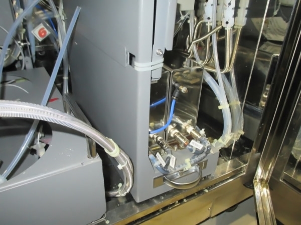

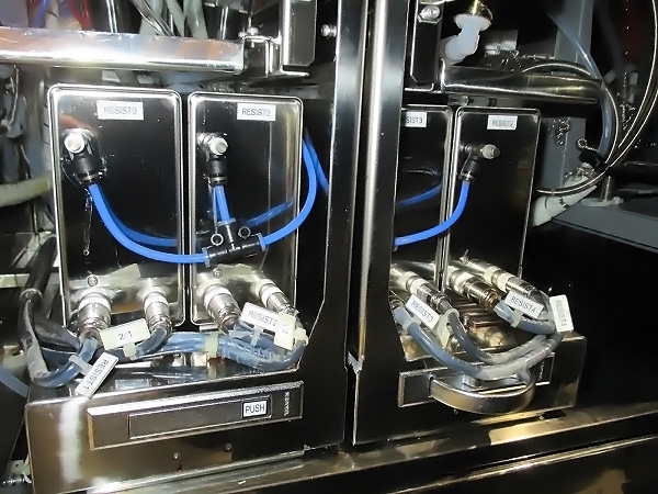

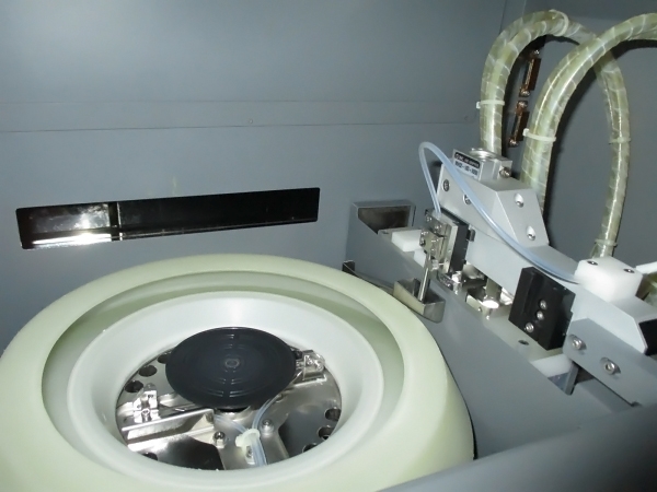

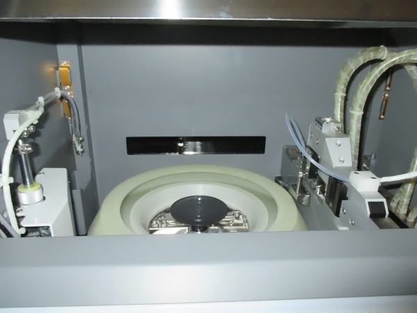

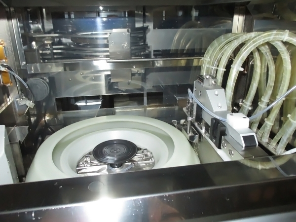


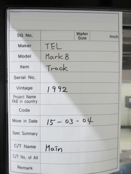

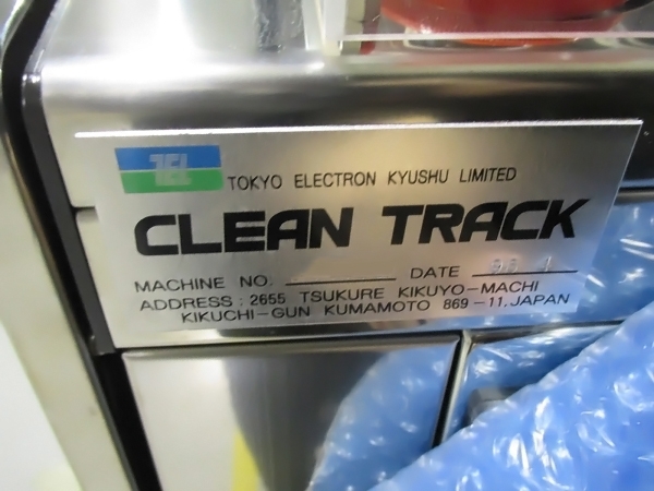

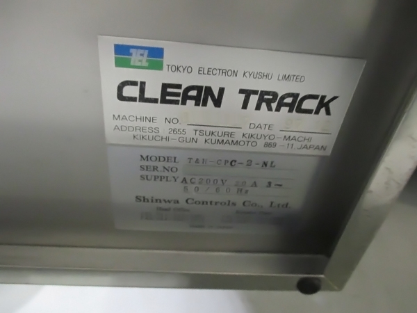

ID: 9215817
Wafer Size: 8"
Vintage: 1996
(2) Coater / (2) Developer system, 8"
4 HP
(4) CP
(3) DHP
(3) 2-1 RRC
EBR Stepping
(2) 2-2 RRC
DEV Flowmeter digital type
E2
I/F NIKON
THC
C/B (3L x4)
LtR
1996 vintage.
TEL / TOKYO ELECTRON Mark 8 is a type of photoresist equipment which utilizes advanced lithographic techniques to facilitate the etching of circuits or other intricate patterns and shapes into substrate materials such as silicon or metal. Specifically, TEL MARK8 photoresist system can be used to insulate the substrate against etching by specifically permitting only selected parts of the substrate to be etched and employing the photoresist layer to protect other parts of the substrate from the chemical etching process. TOKYO ELECTRON MARK-8 photoresist unit involves a two-step process which begins with the deposition of a very thin coating of photoresist onto the substrate. After the application of photoresist, MARK-8 machine then exposes the photoresist to light of a predetermined wavelength, thereby causing a chemical change to occur within the photoresist which enables it to either resist or permit the etching process depending on the thickness of the photoresist coating. The subsequent etching of a pattern into the substrate is then carried out with high-precision beam focusing which is made possible thanks to the state-of-the-art technologies employed by MARK8 photoresist tool. Substrate materials can be protected from etching to a very high degree of accuracy, even with complex patterns and shapes such as those found in integrated circuits and microelectronic devices. Additionally, TOKYO ELECTRON MARK8 asset offers the user a wide range of choice in photoresist solutions, enabling the user to precisely tailor their application for optimal results. In summation, TEL / TOKYO ELECTRON MARK8 is a top-tier photoresist model which allows for the precise etching of intricate patterns and shapes onto substrates such as silicon or metal. The two-step process of photoresist deposition and light exposure results in a chemical transformation of the photoresist layer which either permits or protects against etching, while the advanced beam-focusing capabilities of TEL Mark 8 ensures that the etching process proceeds with a very high level of accuracy. With its comprehensive range of photoresist solutions, Mark 8 is the preferred choice for users looking for reliable, high-precision etching of their substrates.
There are no reviews yet


