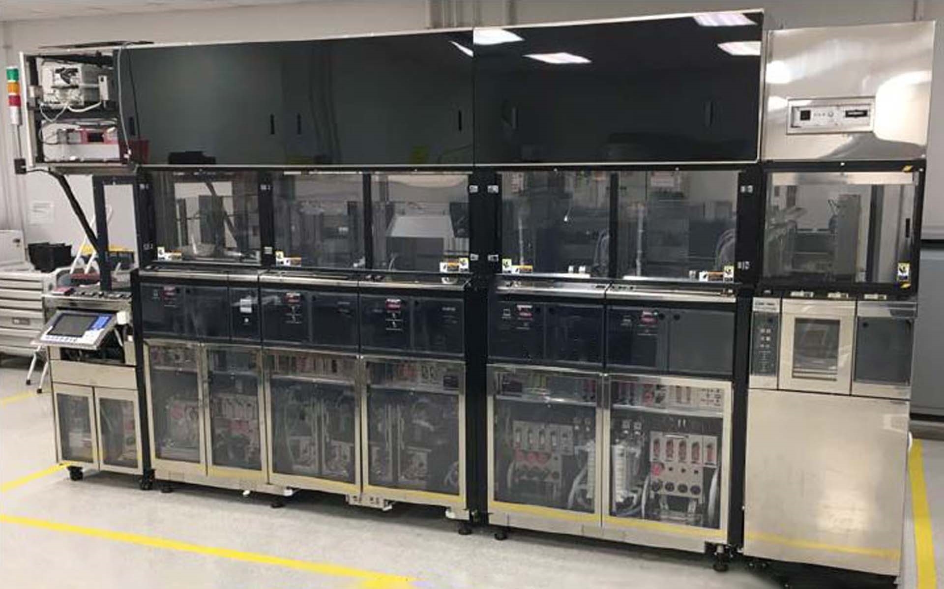
Used TEL / TOKYO ELECTRON Mark 8 #9233994 for sale
It looks like this item has already been sold. Check similar products below or contact us and our experienced team will find it for you.
Tap to zoom


Sold
ID: 9233994
Wafer Size: 8"
System, 8"
Configuration:
SCR
(2) Coater
(2) Developer
DUV Capable
NIKON Stepper interface
(4) RRC (IWAKI T‐100) pumps per coater
(2) E2 Nozzles per developer
(2) Chemical cabinets / TC Racks
SHINWA T&H Unit.
TEL / TOKYO ELECTRON Mark 8 Photoresist Equipment is a state-of-the-art piece of laboratory equipment used for thin film deposition processes commonly seen in the semiconductor industry. The system features an automatic wafer loader that holds up to 200 wafers at a time and a scanning table that enables wafer rotation and accurate wafer positioning. Additionally, TEL MARK8 is equipped with a timer for precise deposition adjustment, a high resolution microscope for monitoring the deposition process in real time, and a wide range of photoresist reservoirs for establishing intricate combinations of thin film structures at the microscopic level. Through a combination of laser-guided sensor technology and mechanized processes, TOKYO ELECTRON MARK-8 Photoresist Unit is able to accurately and efficiently deposit thin films of photoresist material on semiconductor wafers. In order to achieve the desired results, the machine utilizes an array of deposition guns within a vacuum chamber to precisely deposit the photoresist material in a single layer on the wafer. The guns are adjusted so that they use vacuum pressure, precise angles of attack, and varying speeds to provide high levels of accuracy and repeatability when depositing the photoresist material. The vacuum chamber used by TEL / TOKYO ELECTRON MARK8 tool gives users the ability to achieve optimal deposition uniformity and temperature control during the deposition process. Additionally, TEL MARK-8 is able to provide a uniform coating thickness across the wafer by using adjustable nozzle speeds and software-controllable shutter mechanisms for each of the deposition guns. As a result of this precise deposition technology, TEL / TOKYO ELECTRON MARK-8 Photoresist Asset can produce high-quality chipsets and integrated circuits used in digital devices, computers, and other consumer electronics. MARK-8 Photoresist Model provides an extensive set of tools and resources that enable efficient and reliable thin film deposition processes. With its ability to accurately optimize deposition speed and thickness, as well as to precisely monitor the growth of semiconductor wafers, TOKYO ELECTRON MARK8 equipment offers excellent repeatability and variances that are smaller than 0.1 nanometers. This system provides a reliable and cost effective way of optimizing semiconductor lithography and deposition processes, resulting in the production of higher quality chipsets and electronic components.
There are no reviews yet