Used TEL / TOKYO ELECTRON Mark 8 #9275964 for sale
URL successfully copied!
Tap to zoom
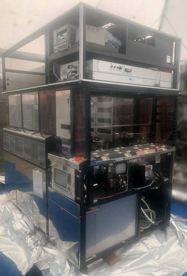

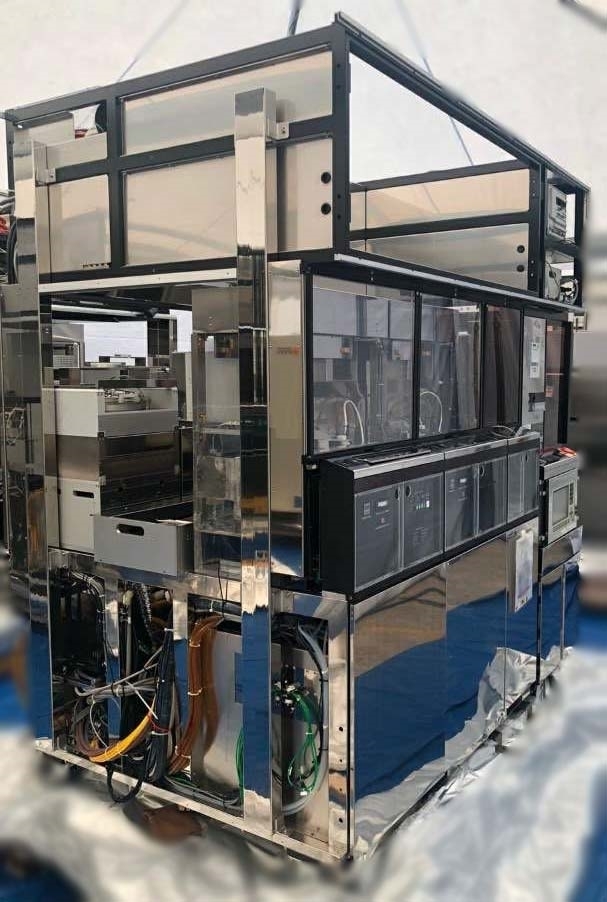

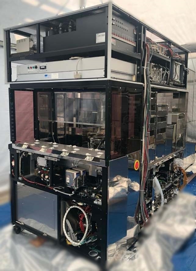

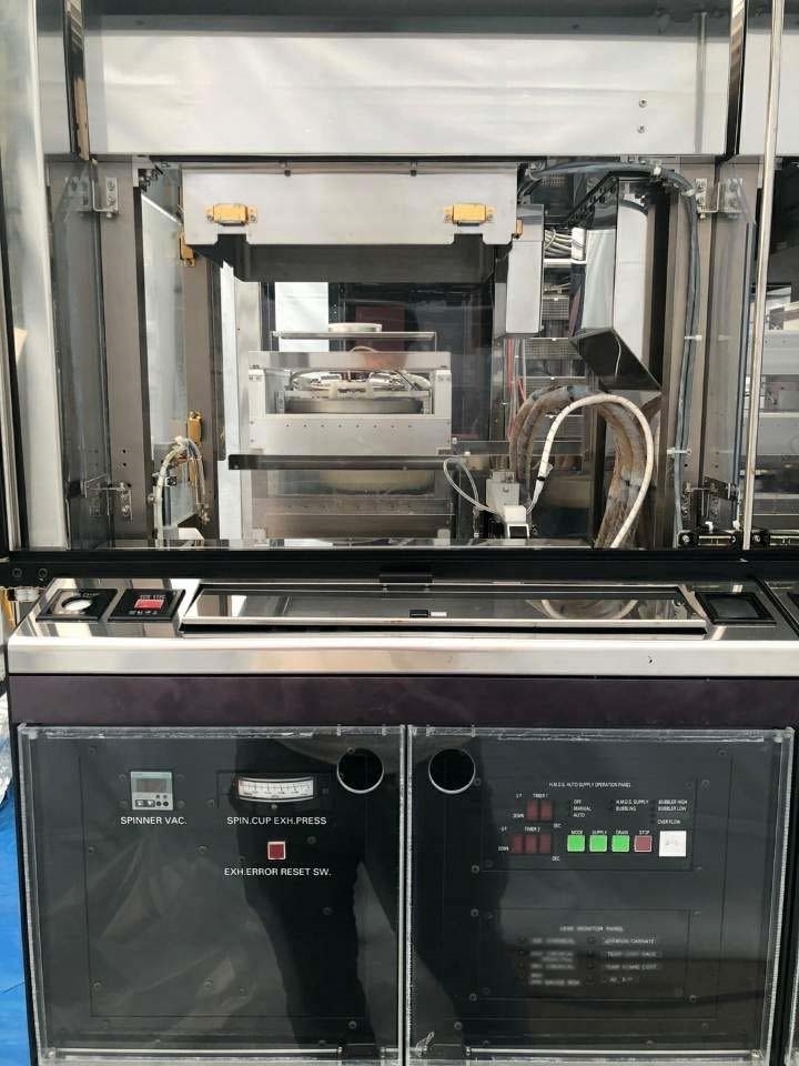

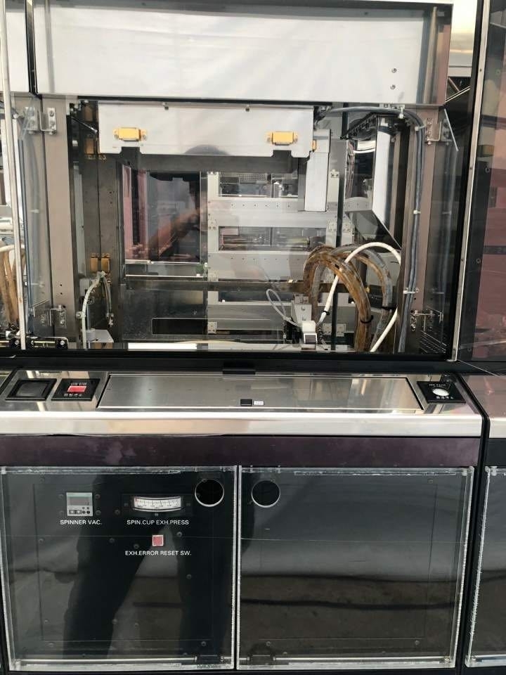

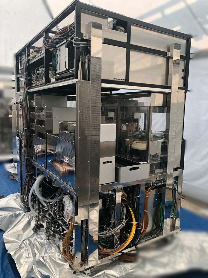

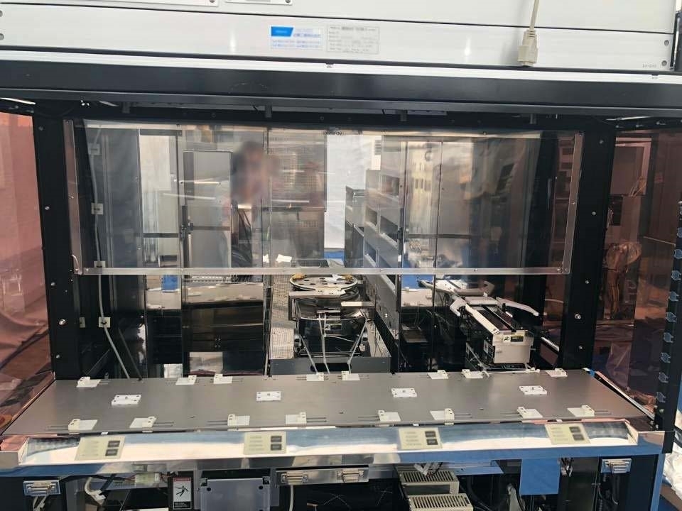

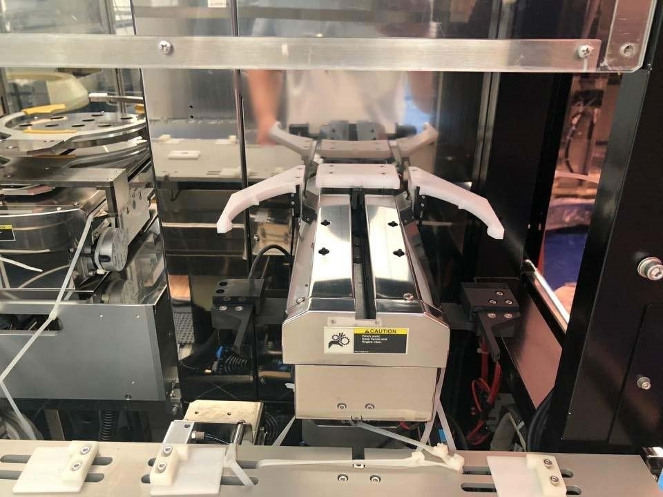

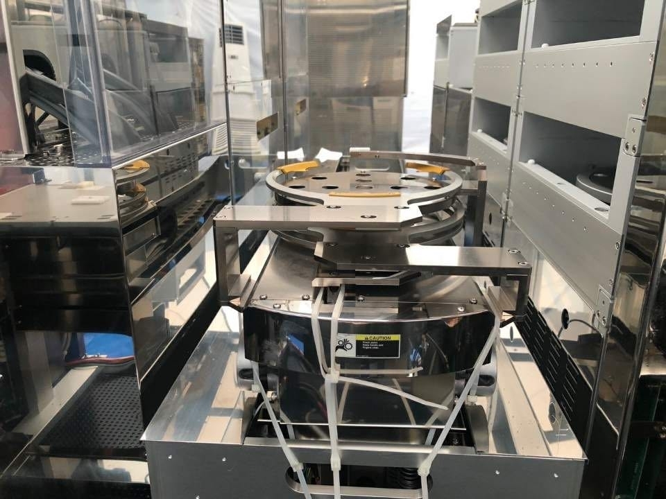

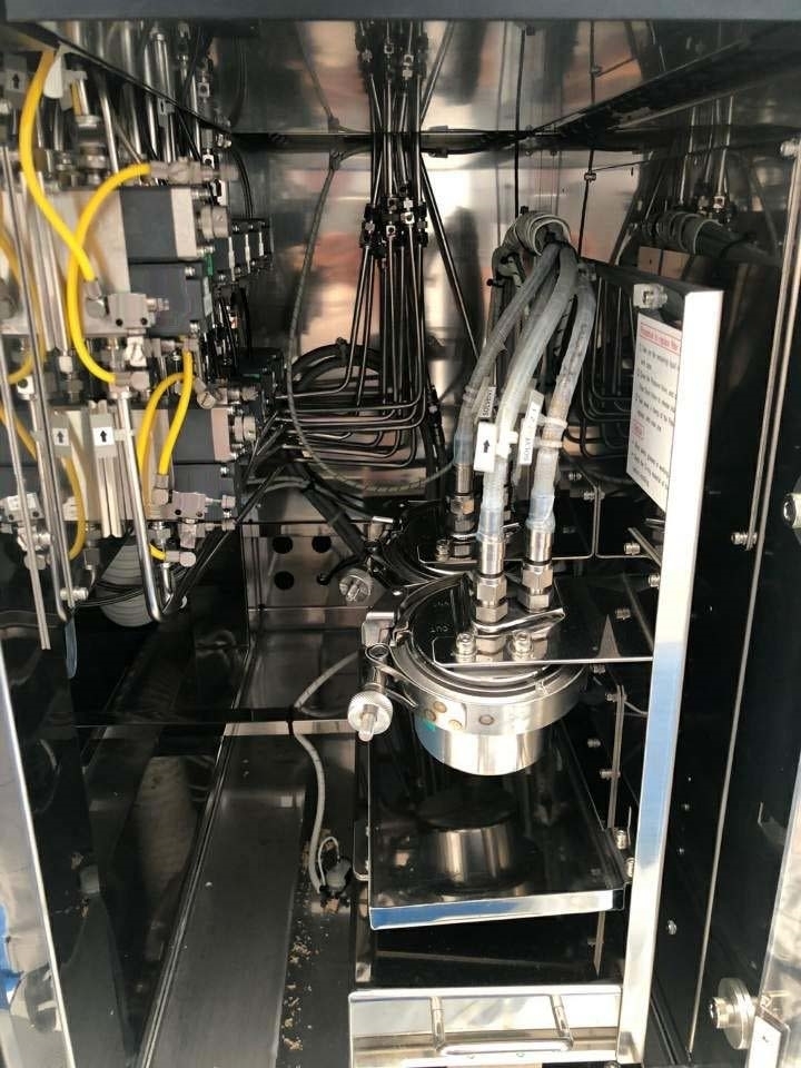

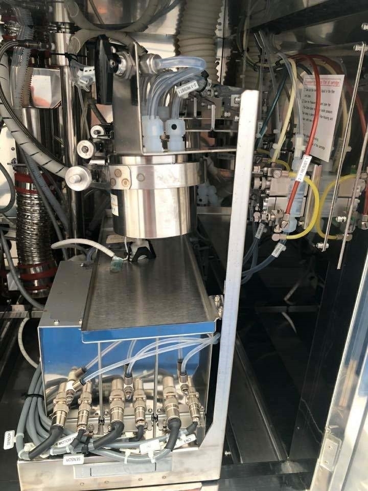

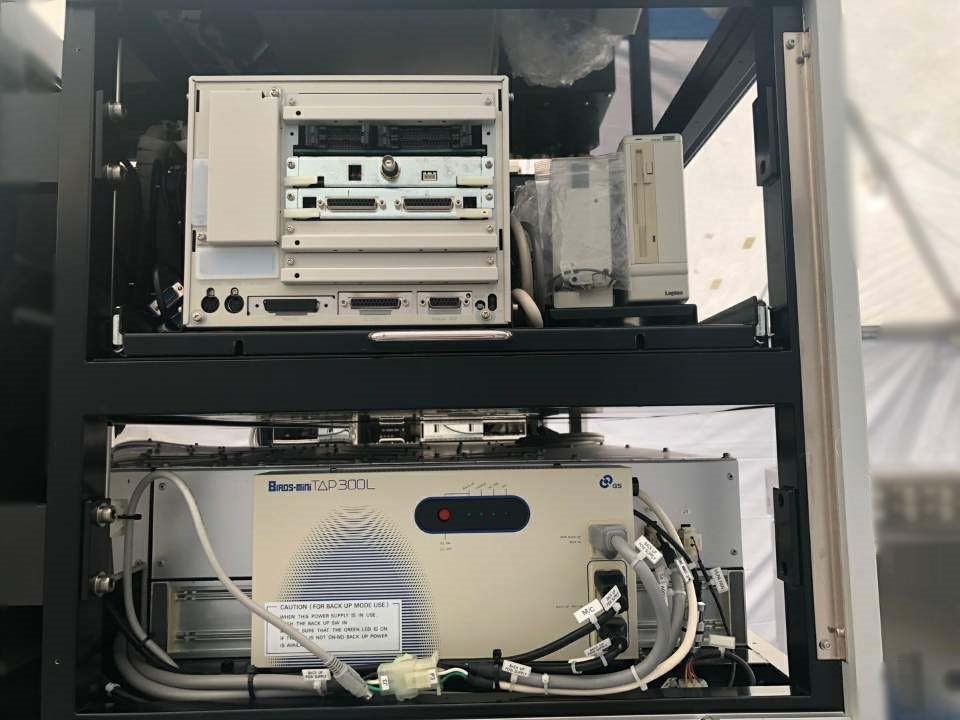

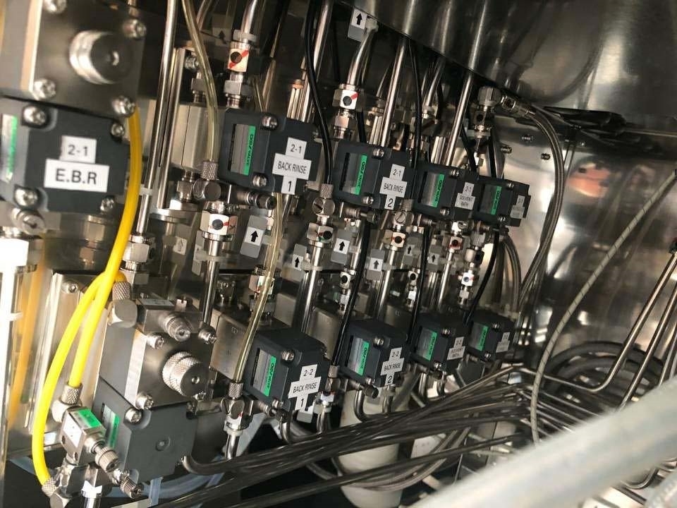


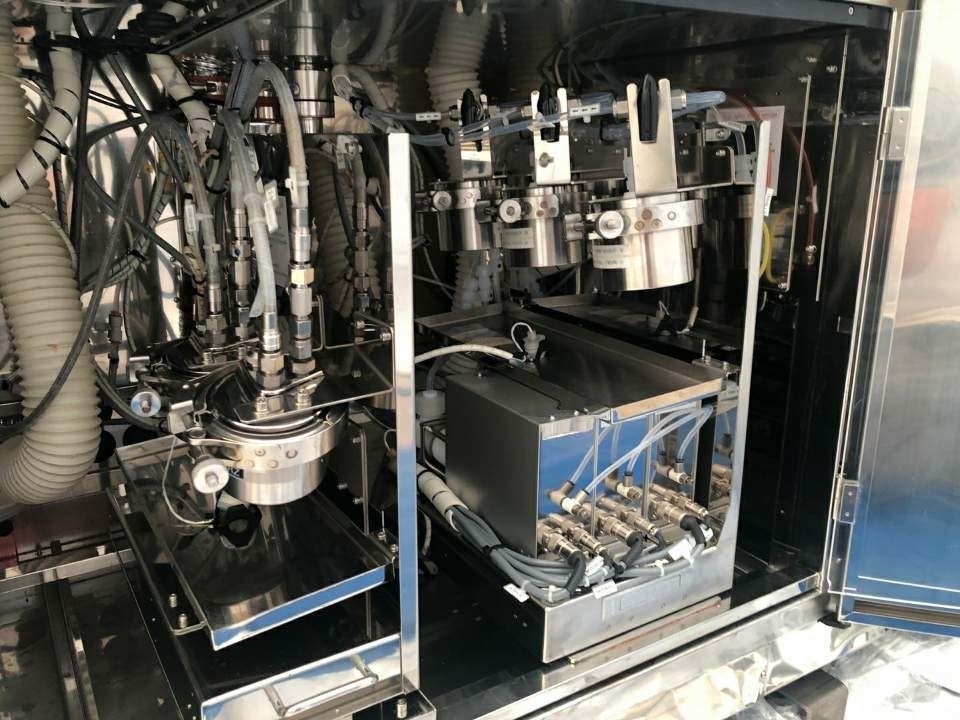

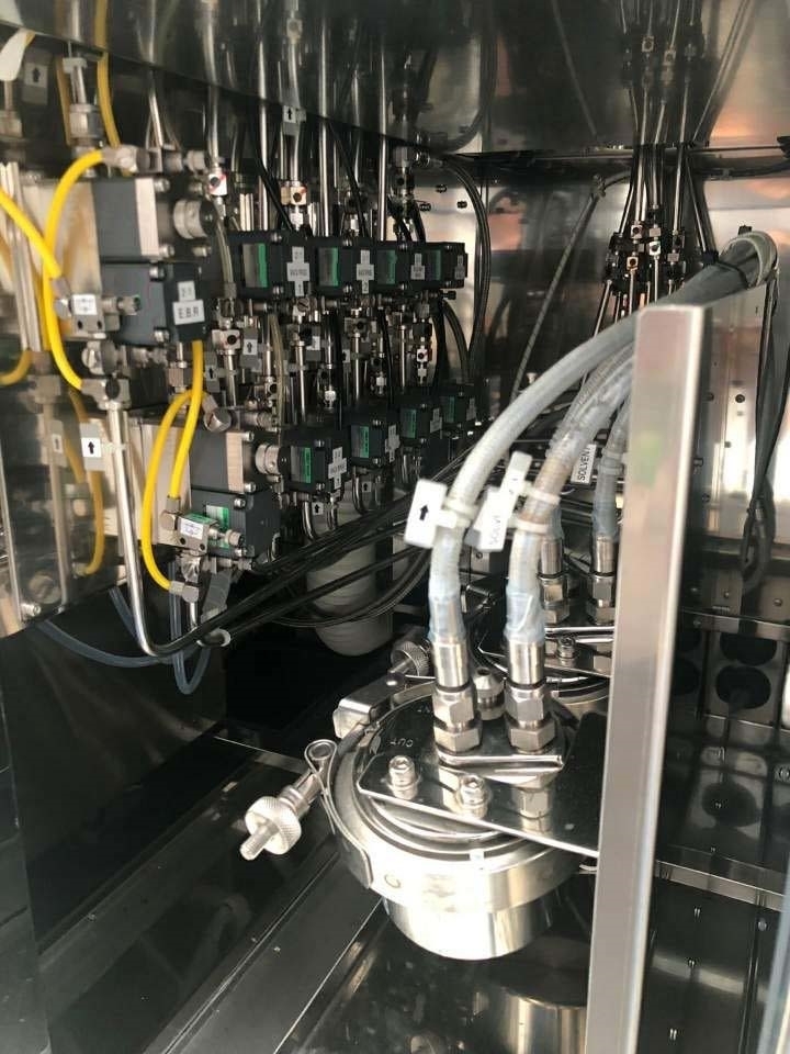

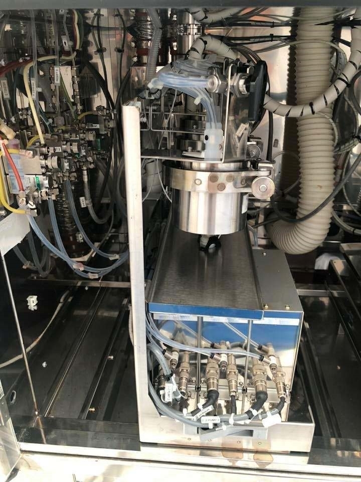

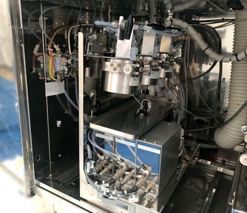

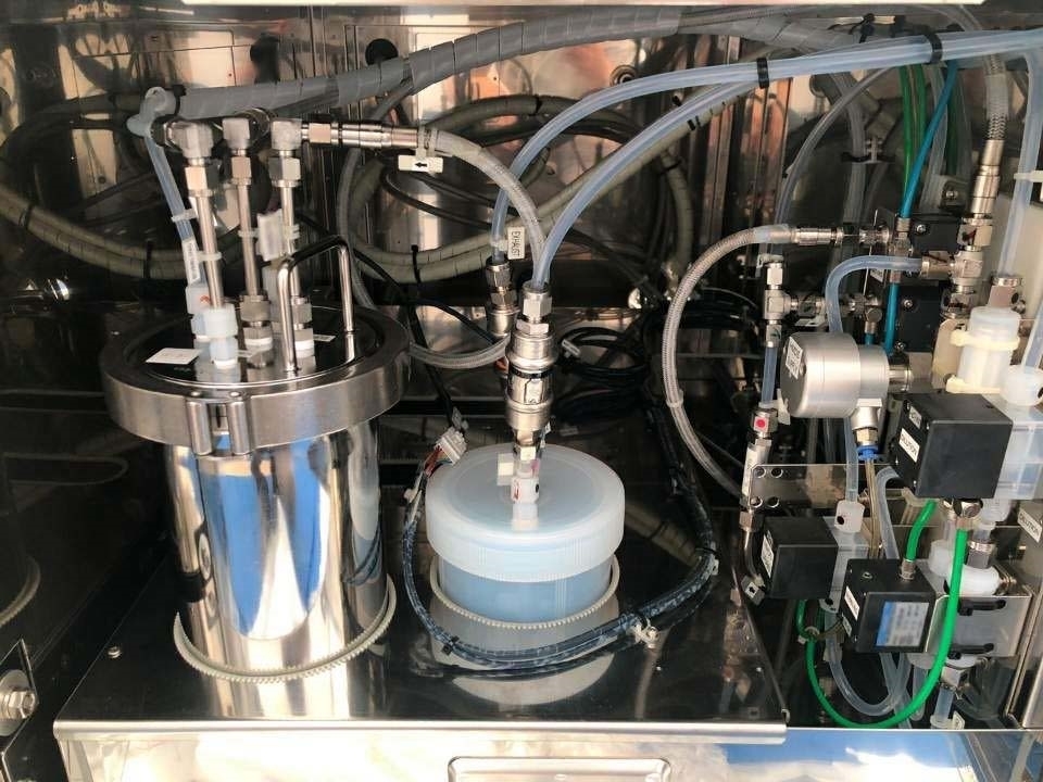

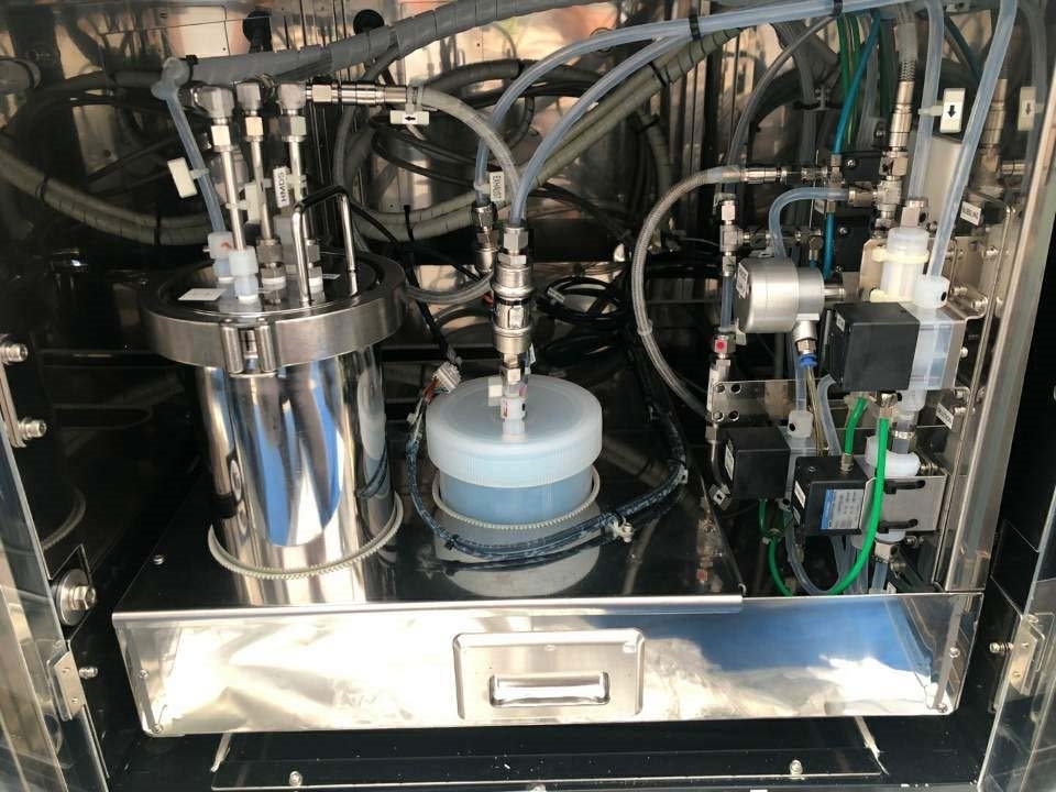

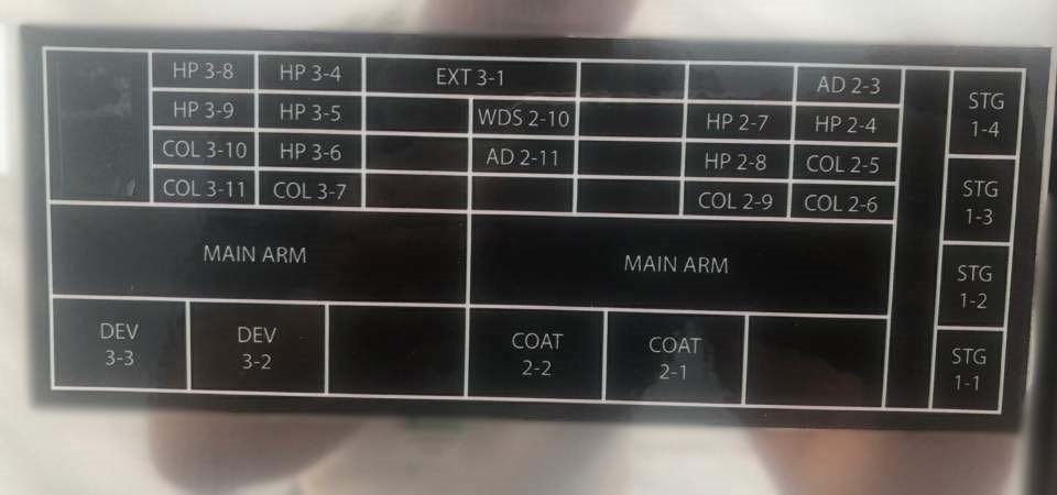

TEL / TOKYO ELECTRON Mark 8 is a photoresist equipment designed for circuit patterning in the fabrication of semiconductor chips. It uses a UV light source to expose a photosensitive film mask over the chip substrate, where the desired circuitry pattern is to be created. The exposed photoresist film is then etched with a chemical developer, removing the unnecessary material to create the circuit pattern on the underlying substrate. TEL MARK8 features a high-resolution laser source, able to provide line widths of 0.3 microns or better. The imaging system of TOKYO ELECTRON MARK-8 employs a multiple-column projection unit with several columns, allowing most line patterns to be accurately and quickly created. A wide variety of mask shapes and patterns can be used with TEL / TOKYO ELECTRON MARK8, and these masks can be changed quickly and easily for different substrate patterns. TEL Mark 8 uses a variety of tools to help ensure the highest quality of the fabricated device. These tools include a scanning electron microscope, which helps scan the exposed substrate to detect defects. Automatic exposure control allows for automatic correction of exposure characteristics, ensuring high-accuracy in the exposure process. The automatic alignment machine enables precise alignment of the mask with the substrate, and the tool can be easily aligned in either X or Y directions. TEL / TOKYO ELECTRON MARK-8 can be used for a wide range of applications, such as semiconductor logic, memory, analog, and power ICs. With a tight control on the fabrication process, TOKYO ELECTRON Mark 8 provided high-quality results with smaller line size and excellent lithography accuracy. The photoresist asset is reliable, repeatable, and easy to use, making it a preferred choice for semiconductor manufacturing.
There are no reviews yet


