Used TEL / TOKYO ELECTRON MARK II #293592869 for sale
URL successfully copied!
Tap to zoom
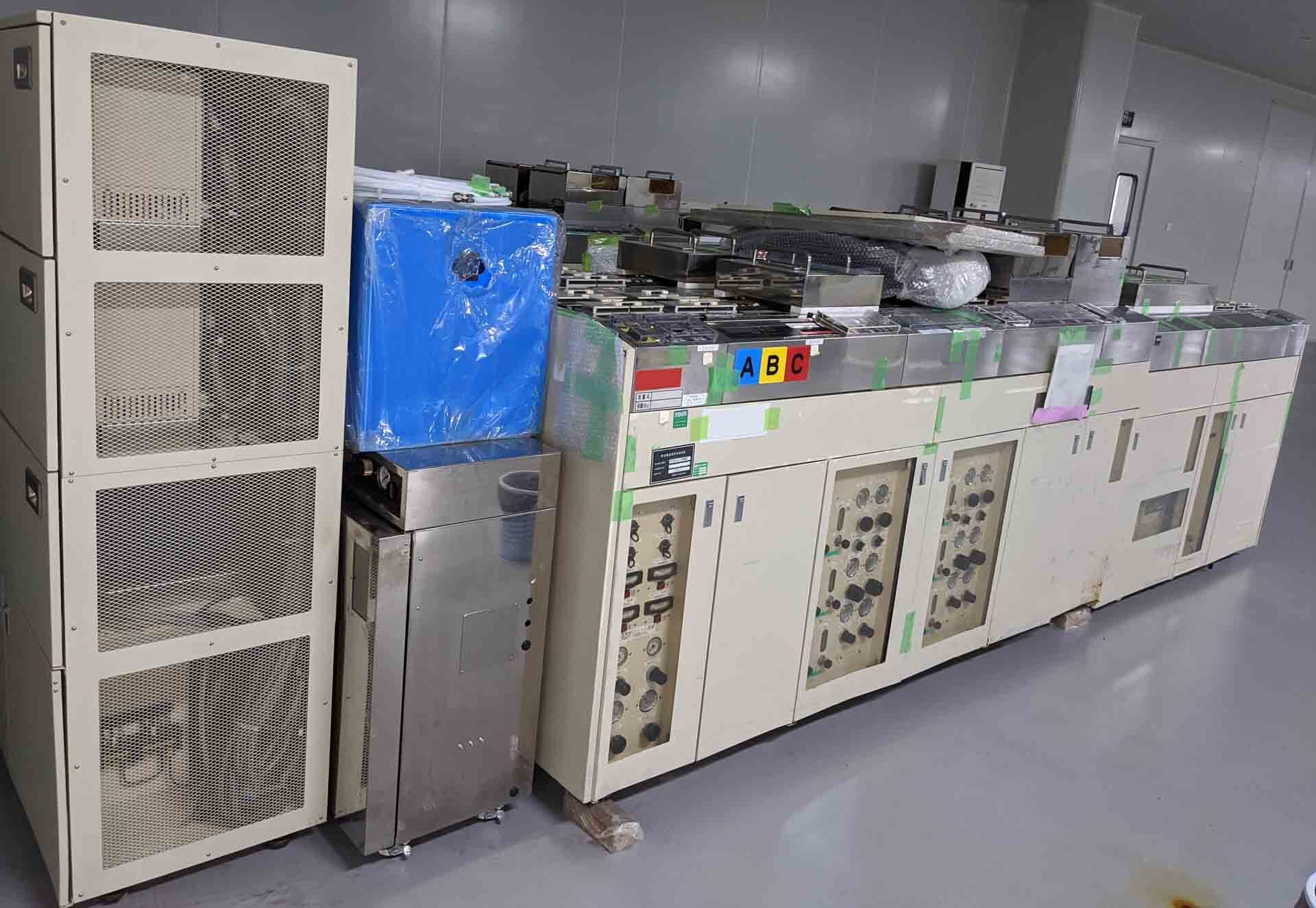

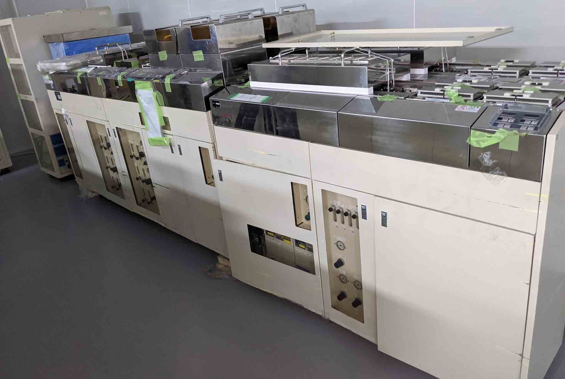

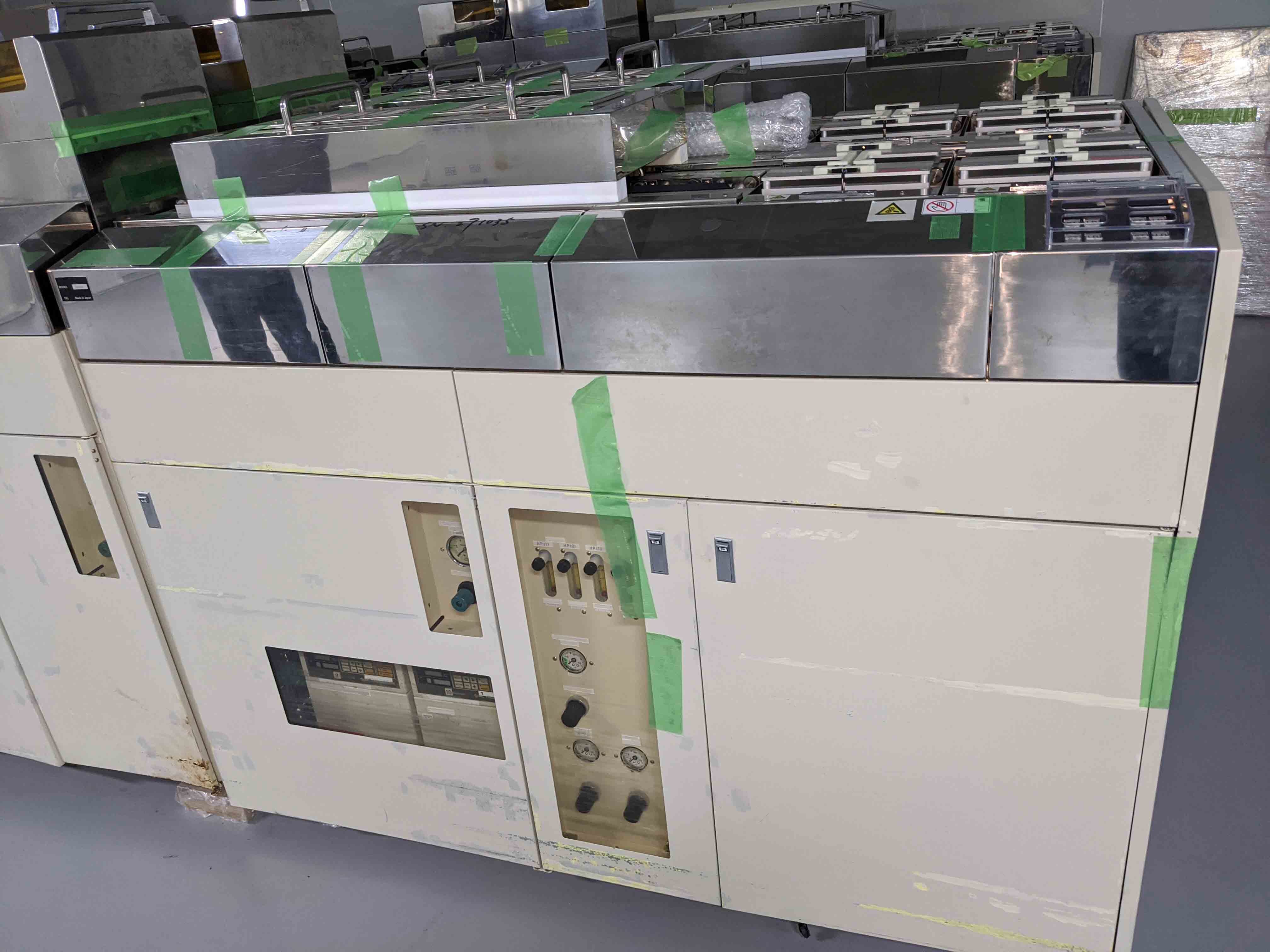

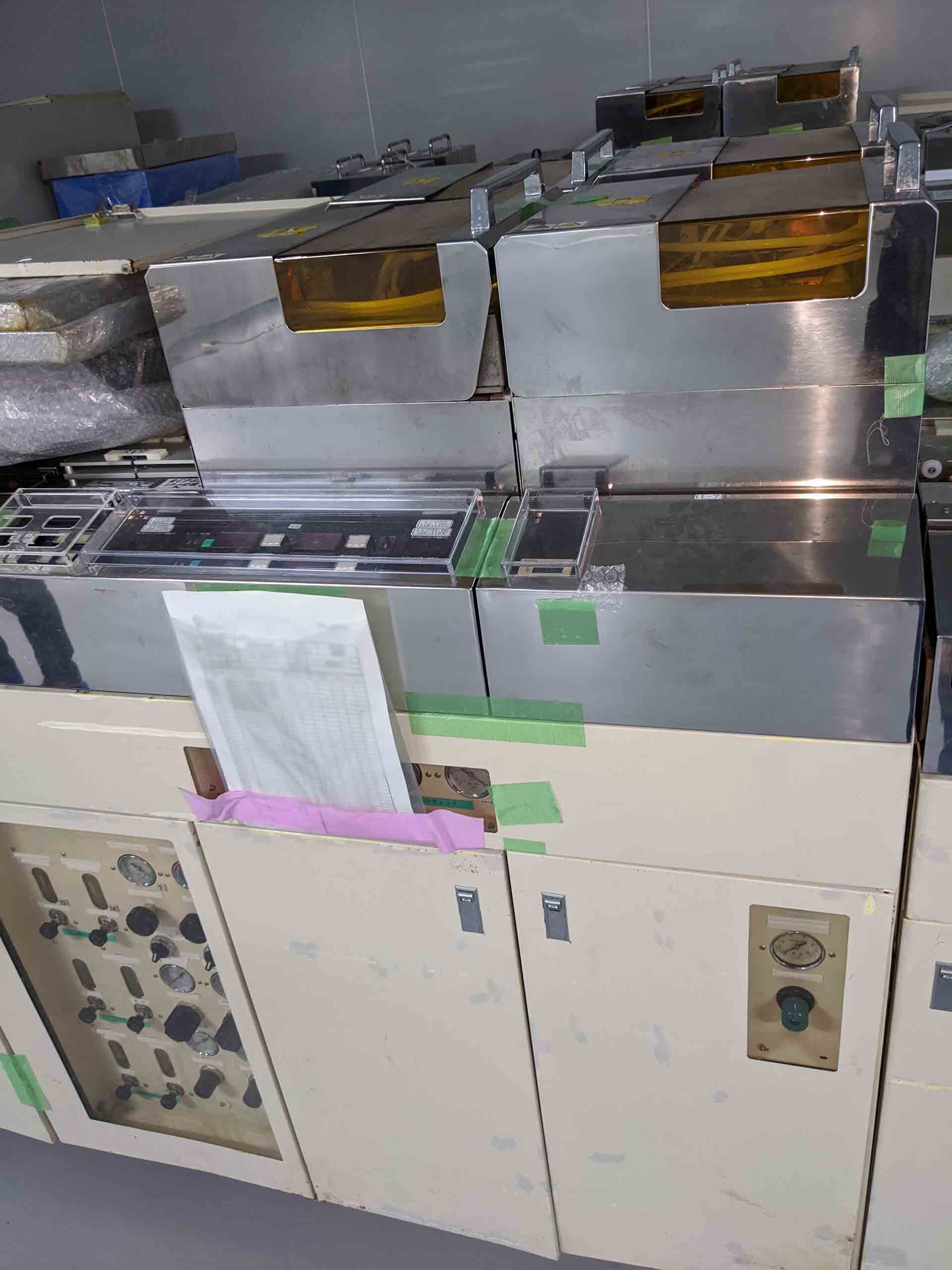

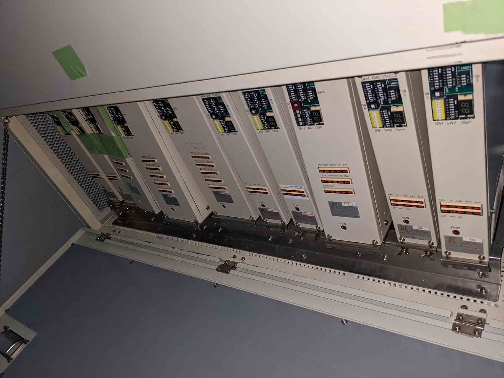

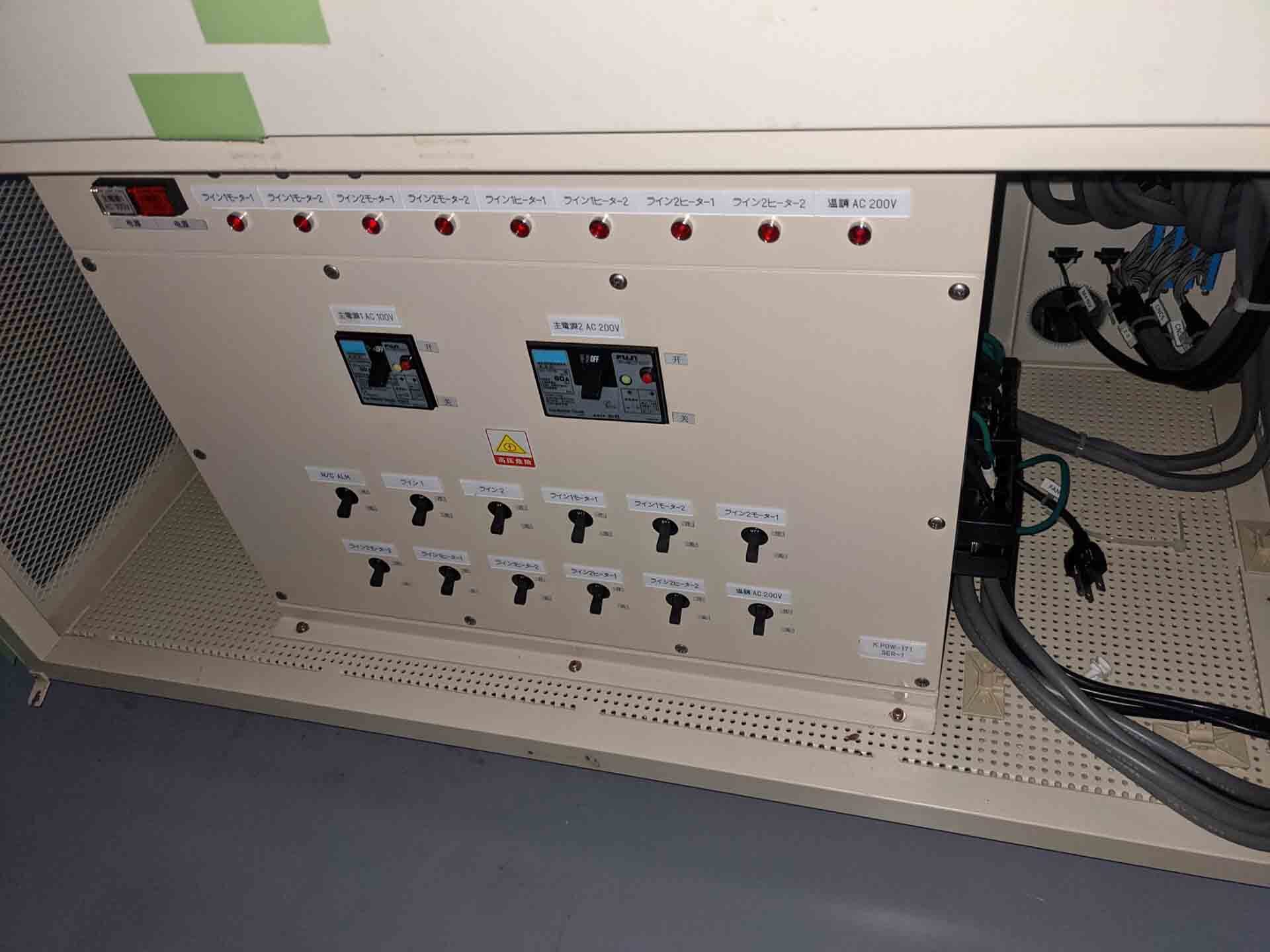

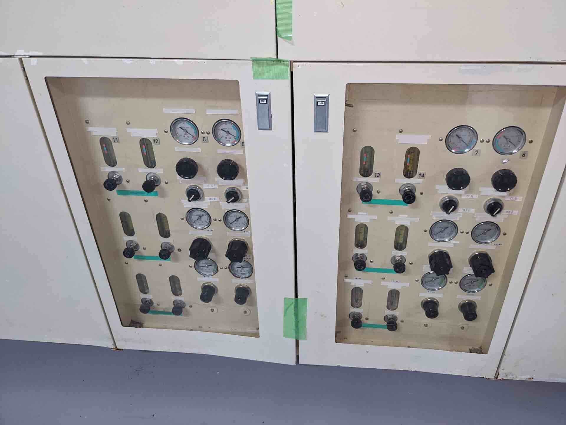

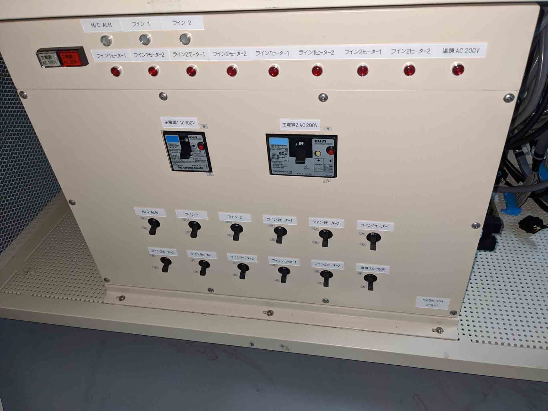

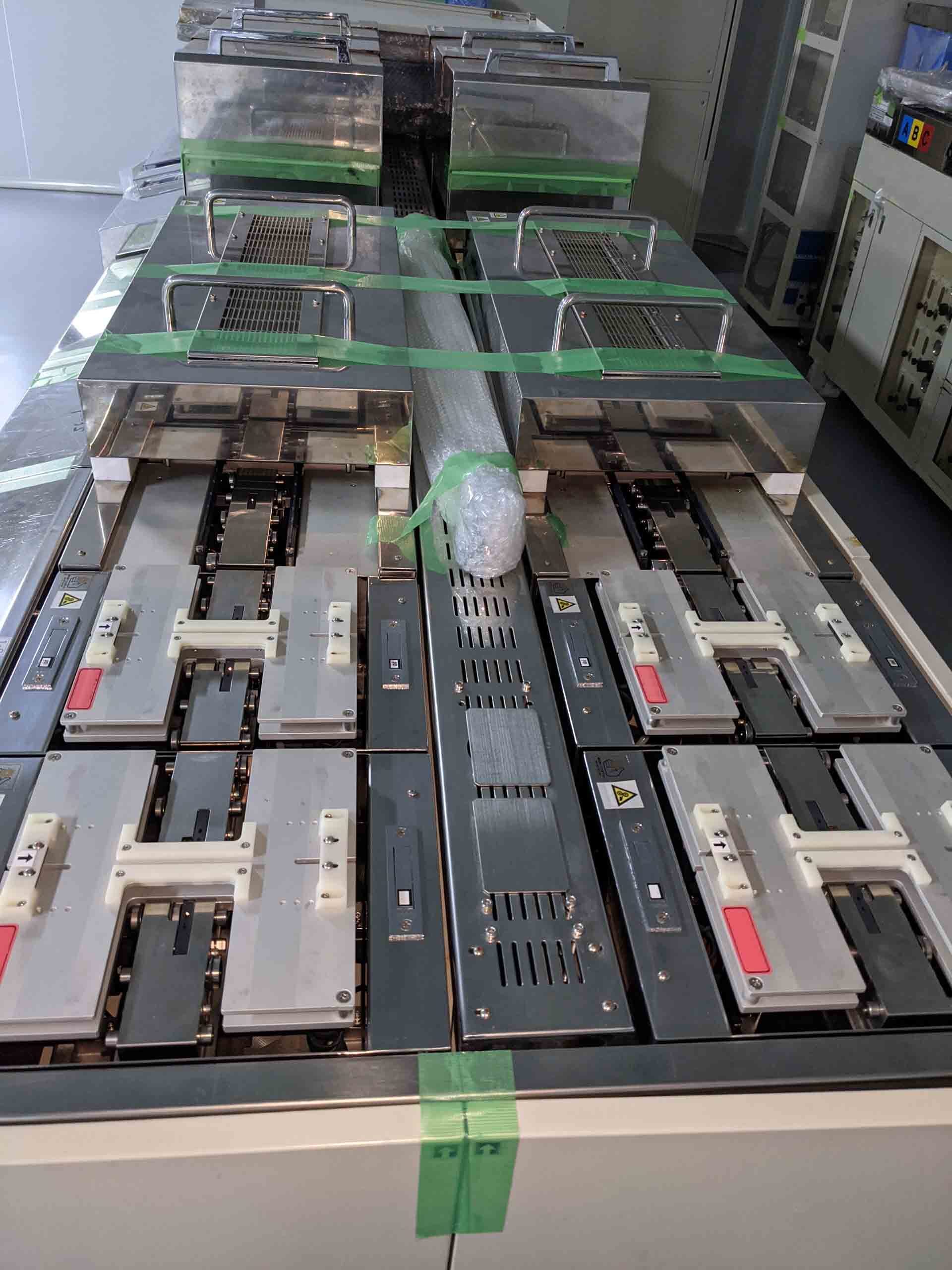

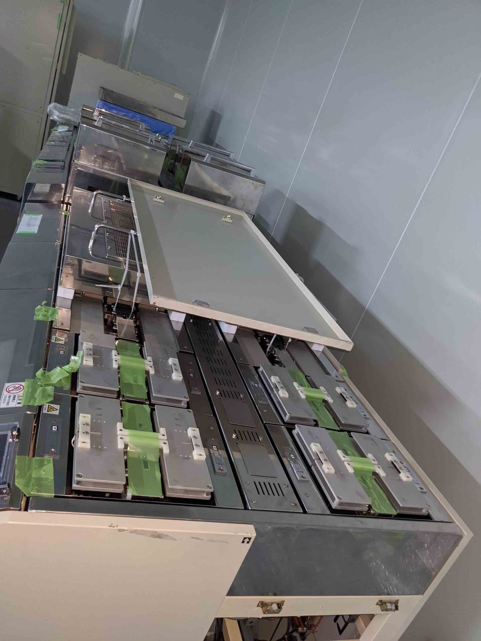

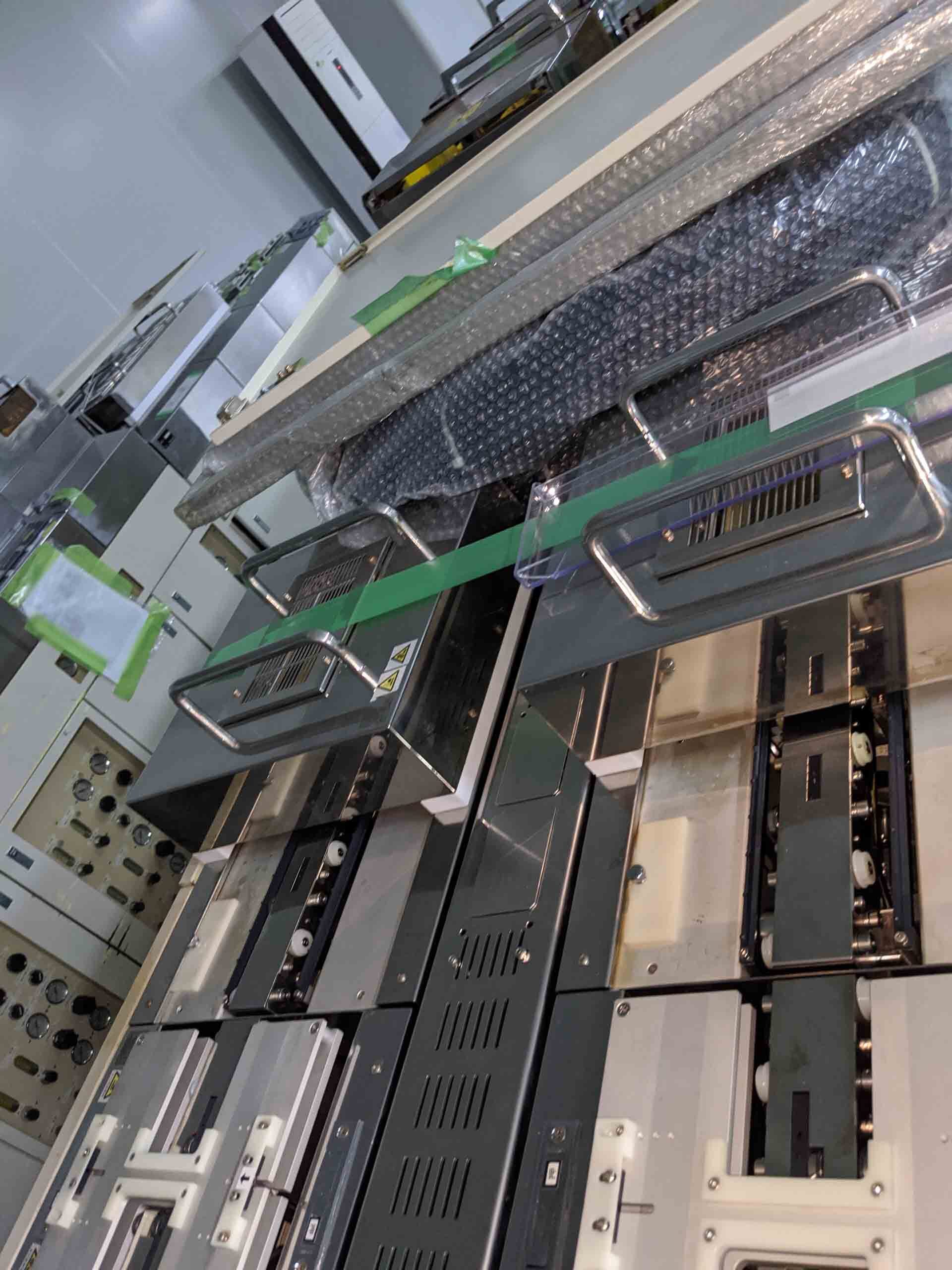

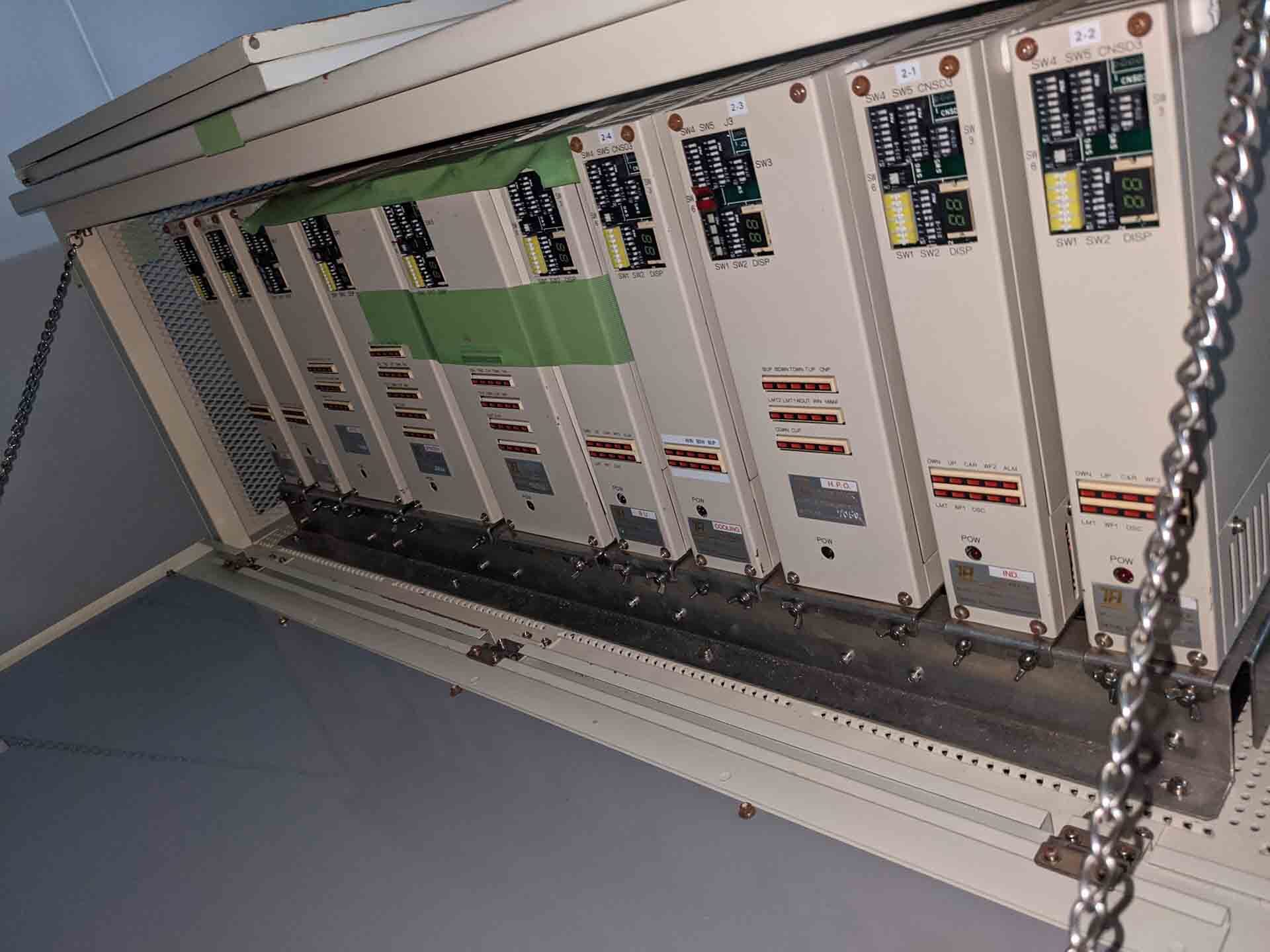

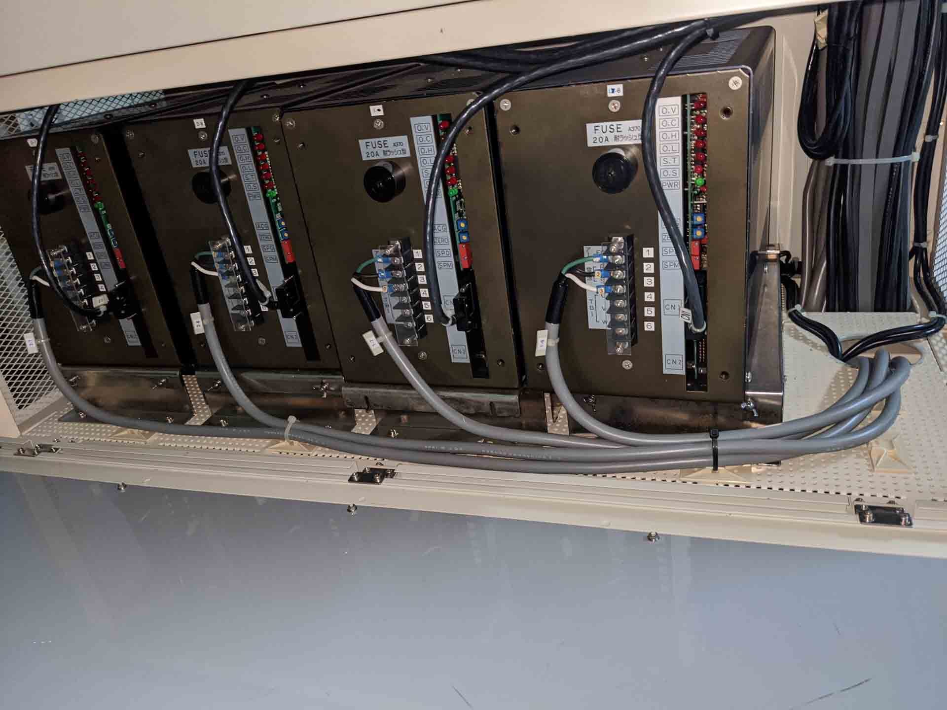

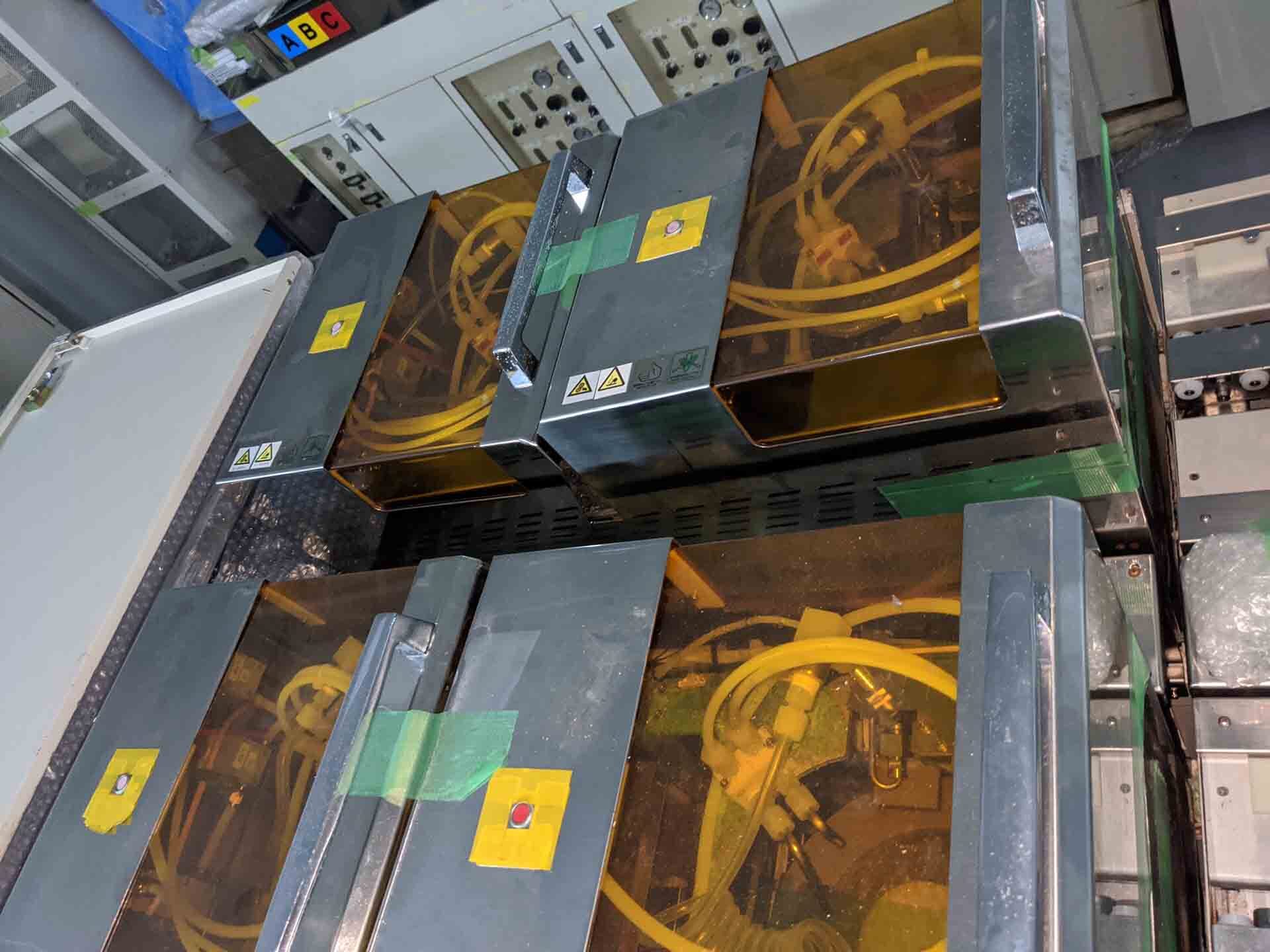


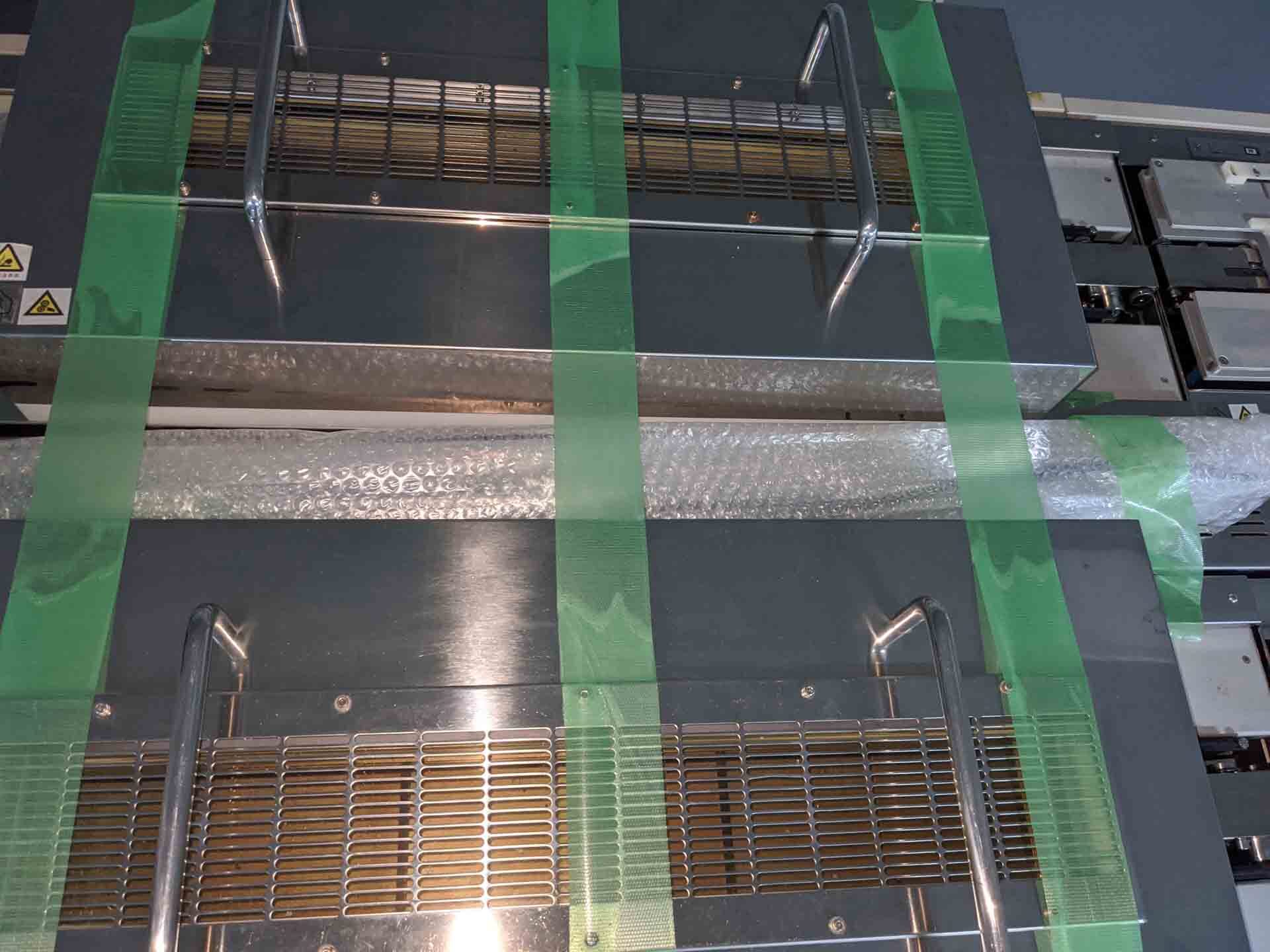

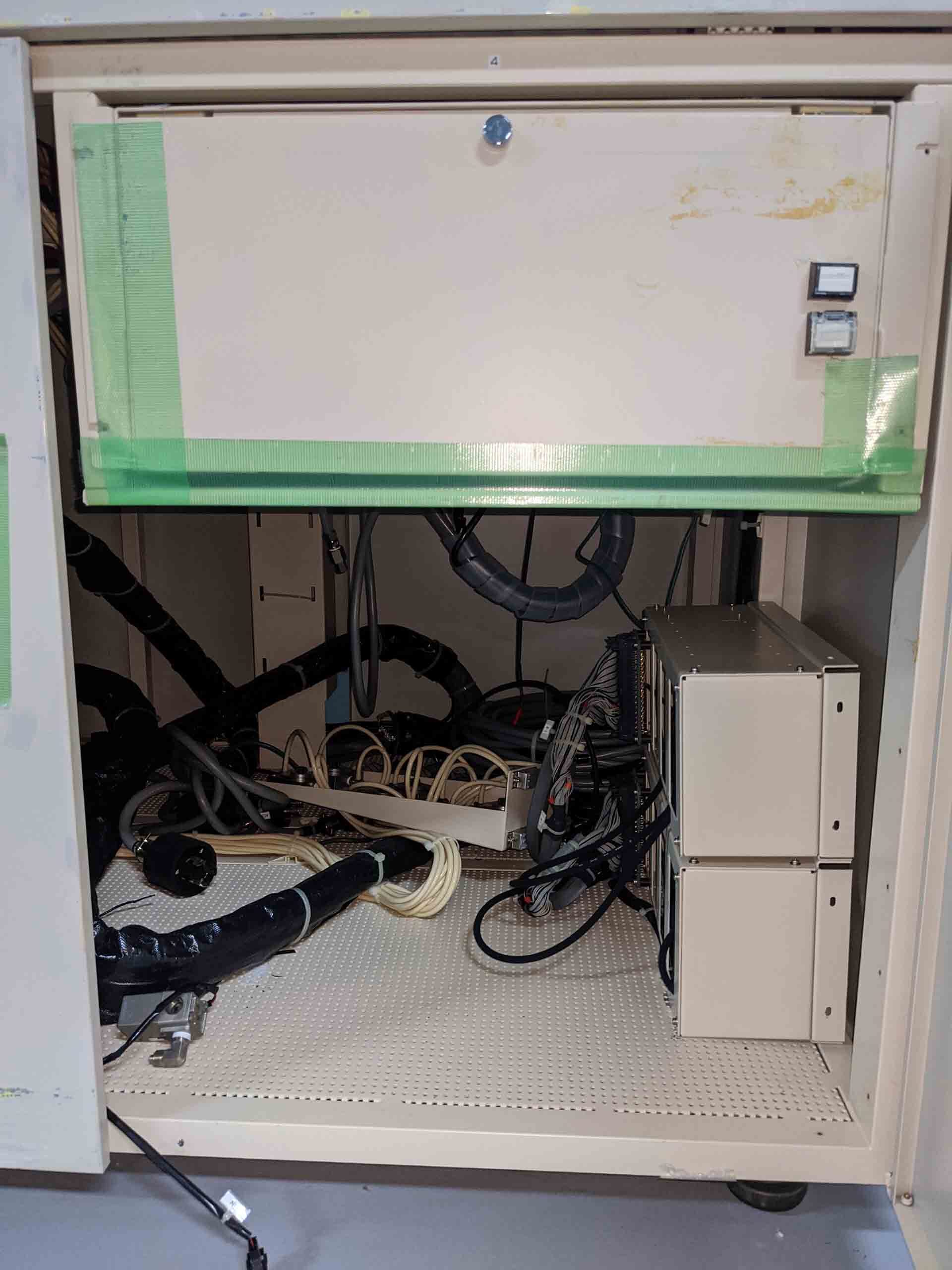


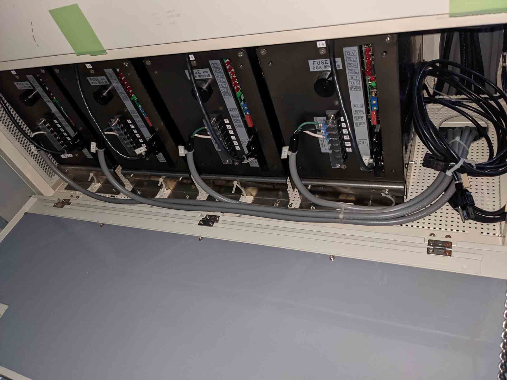

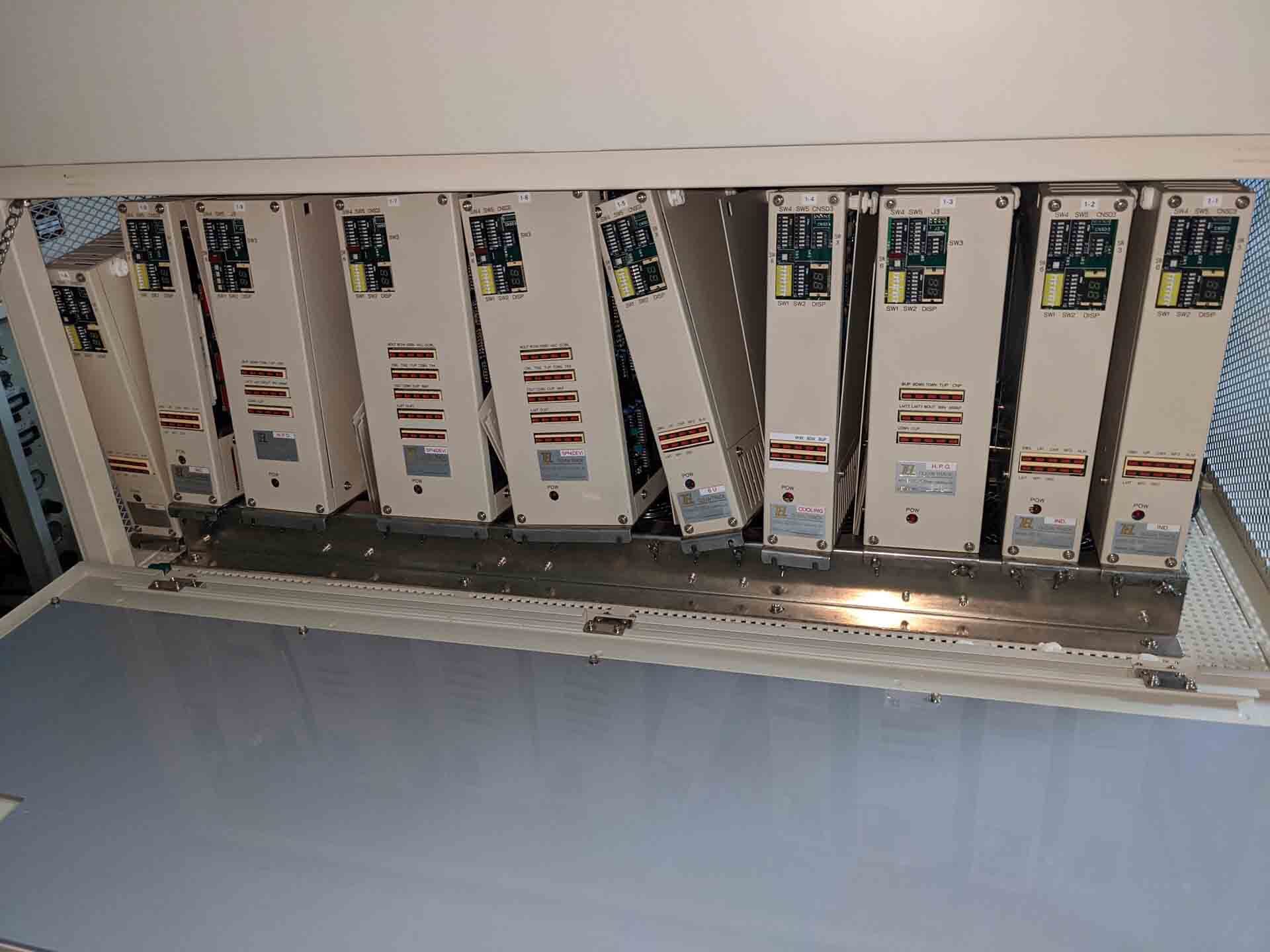

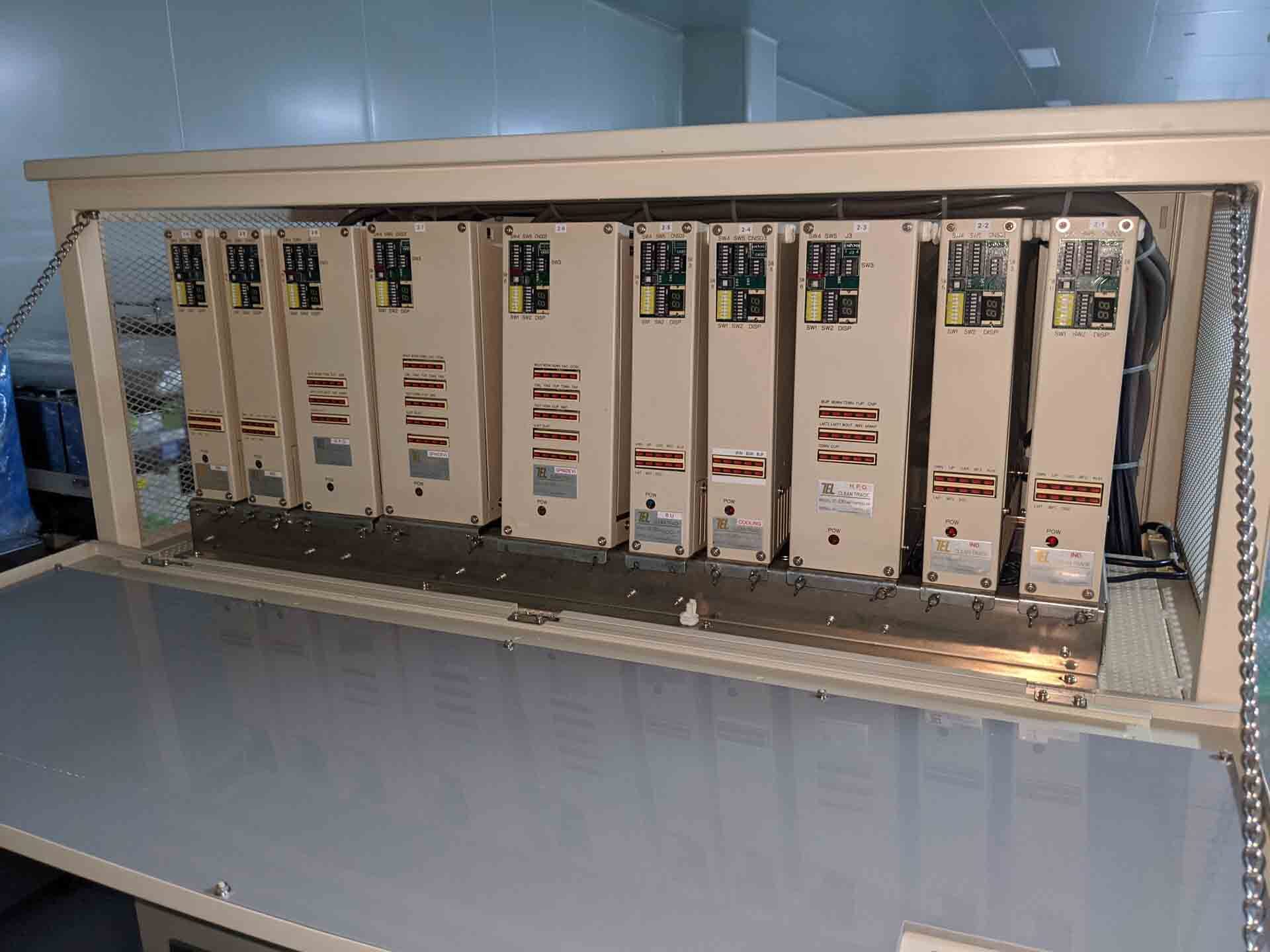


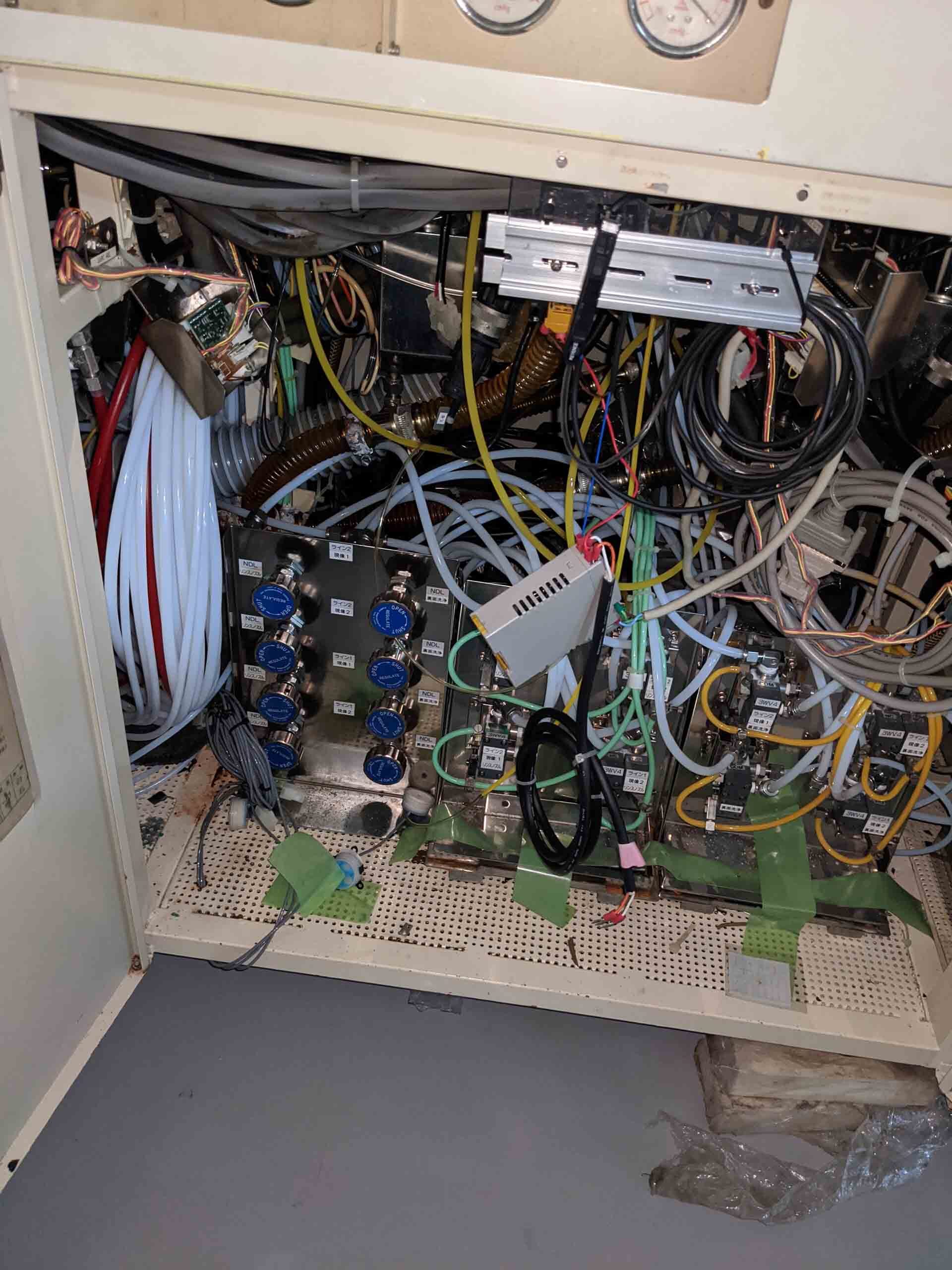



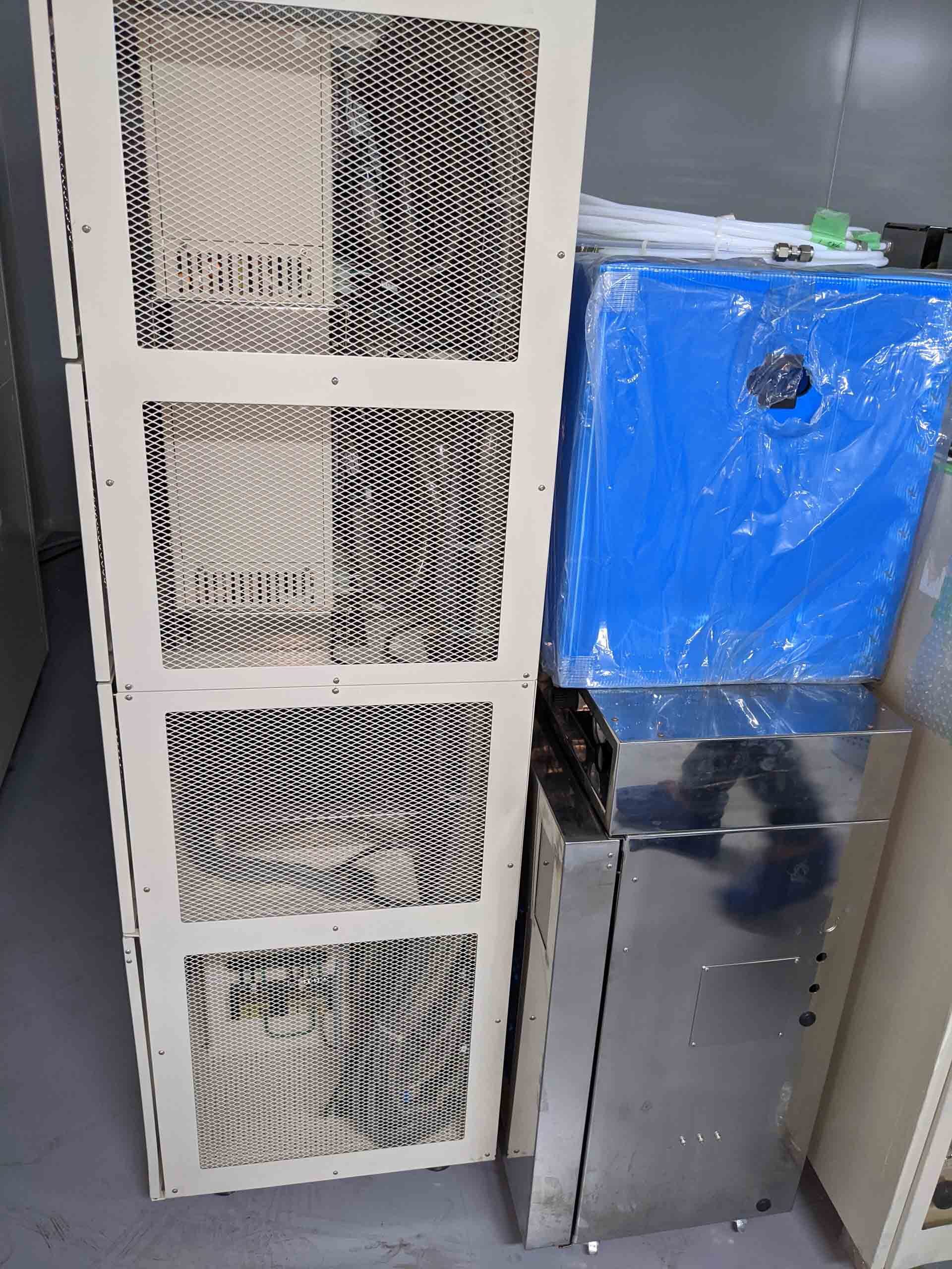

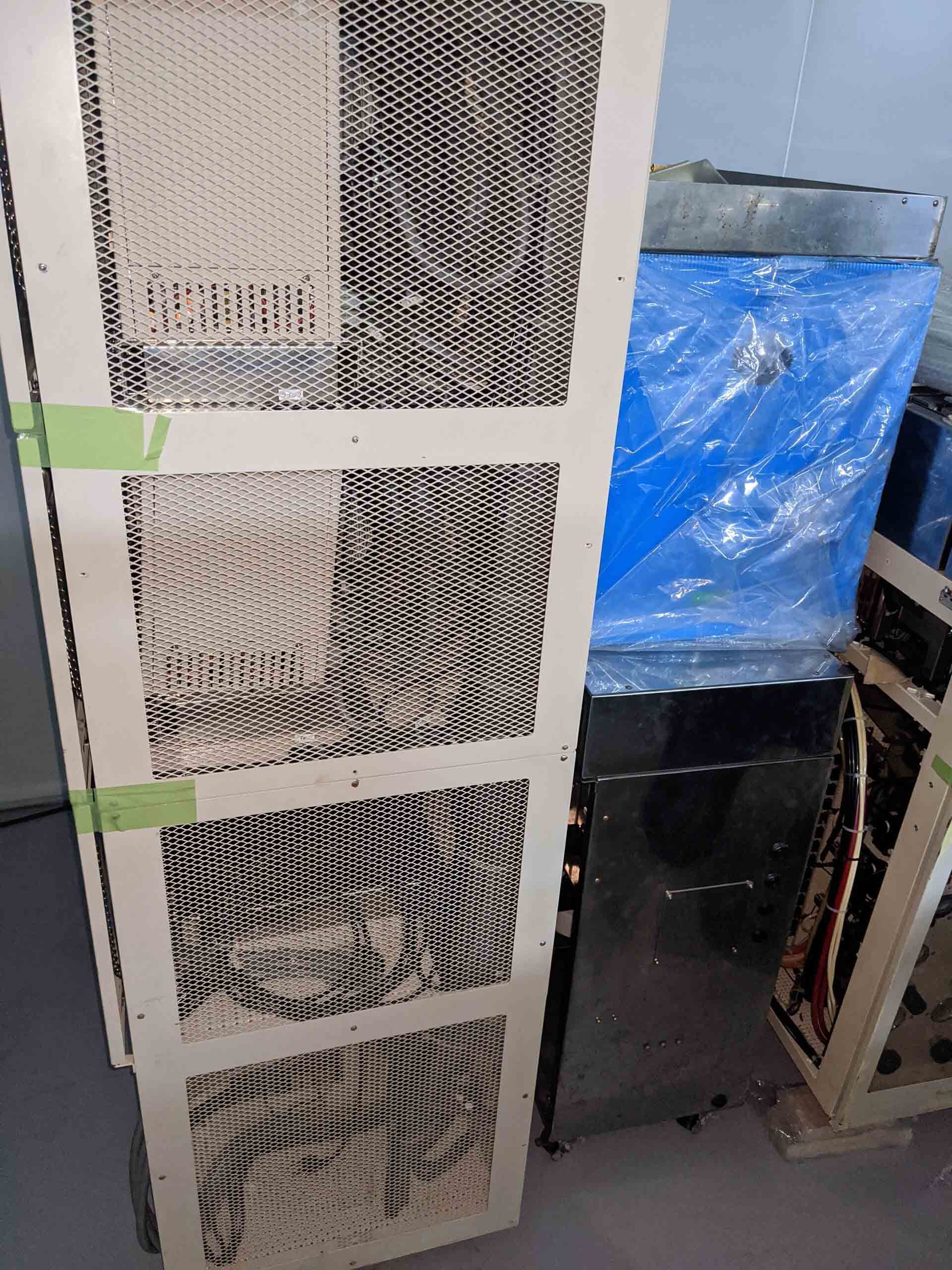

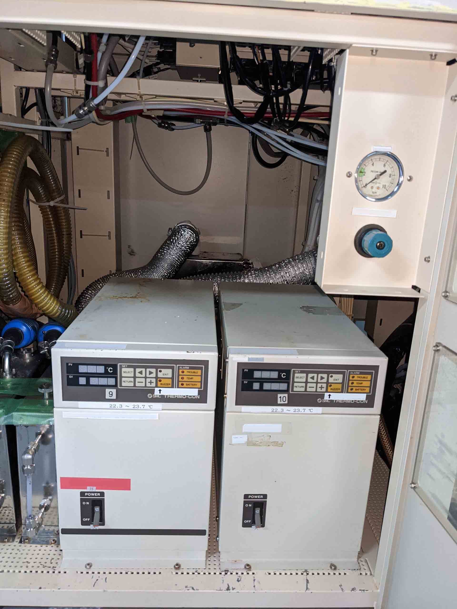

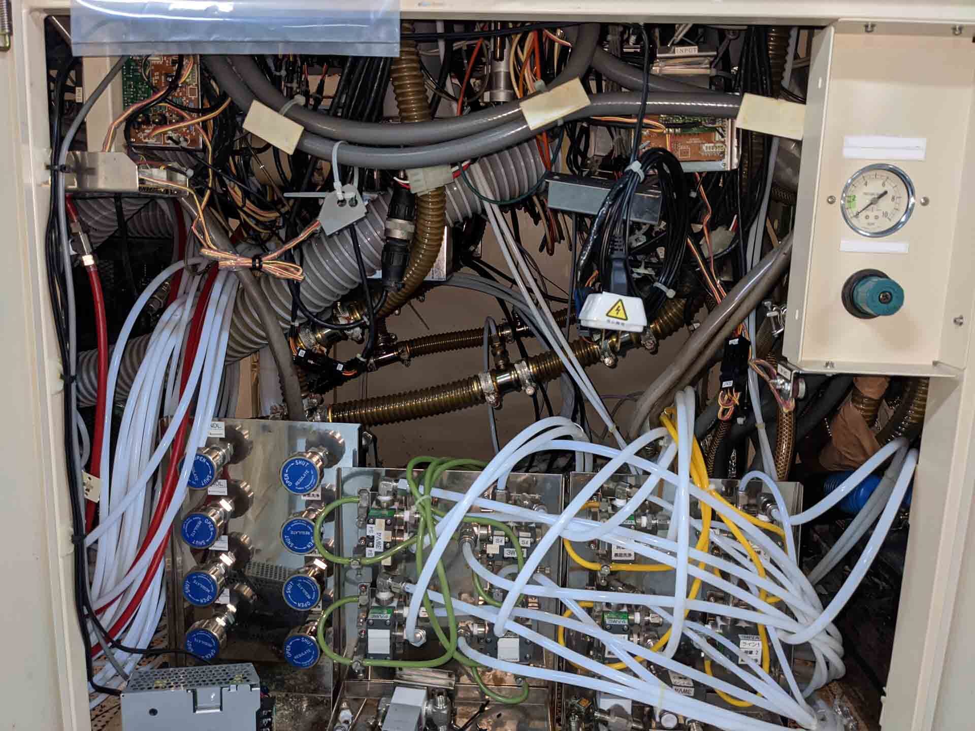

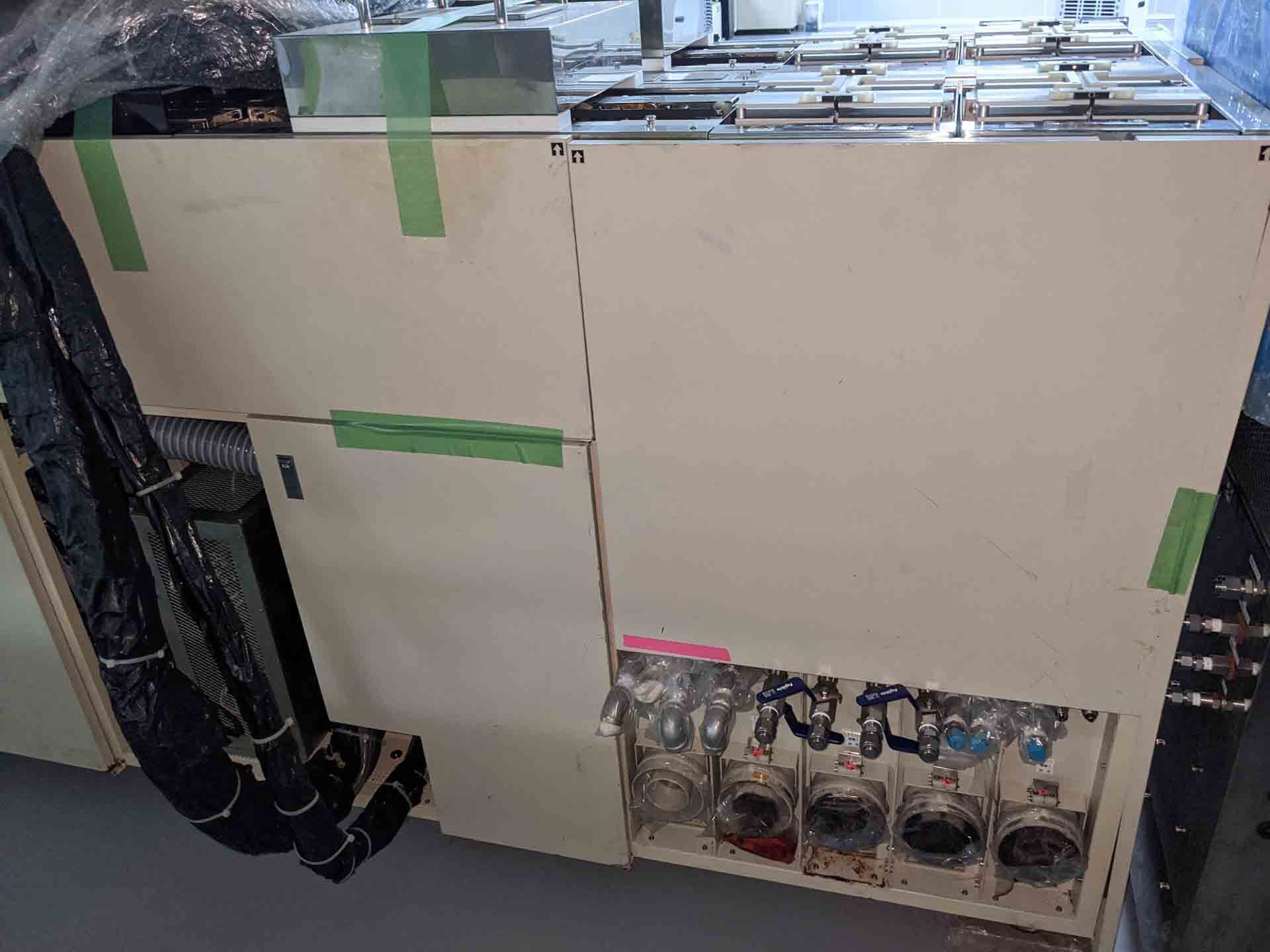

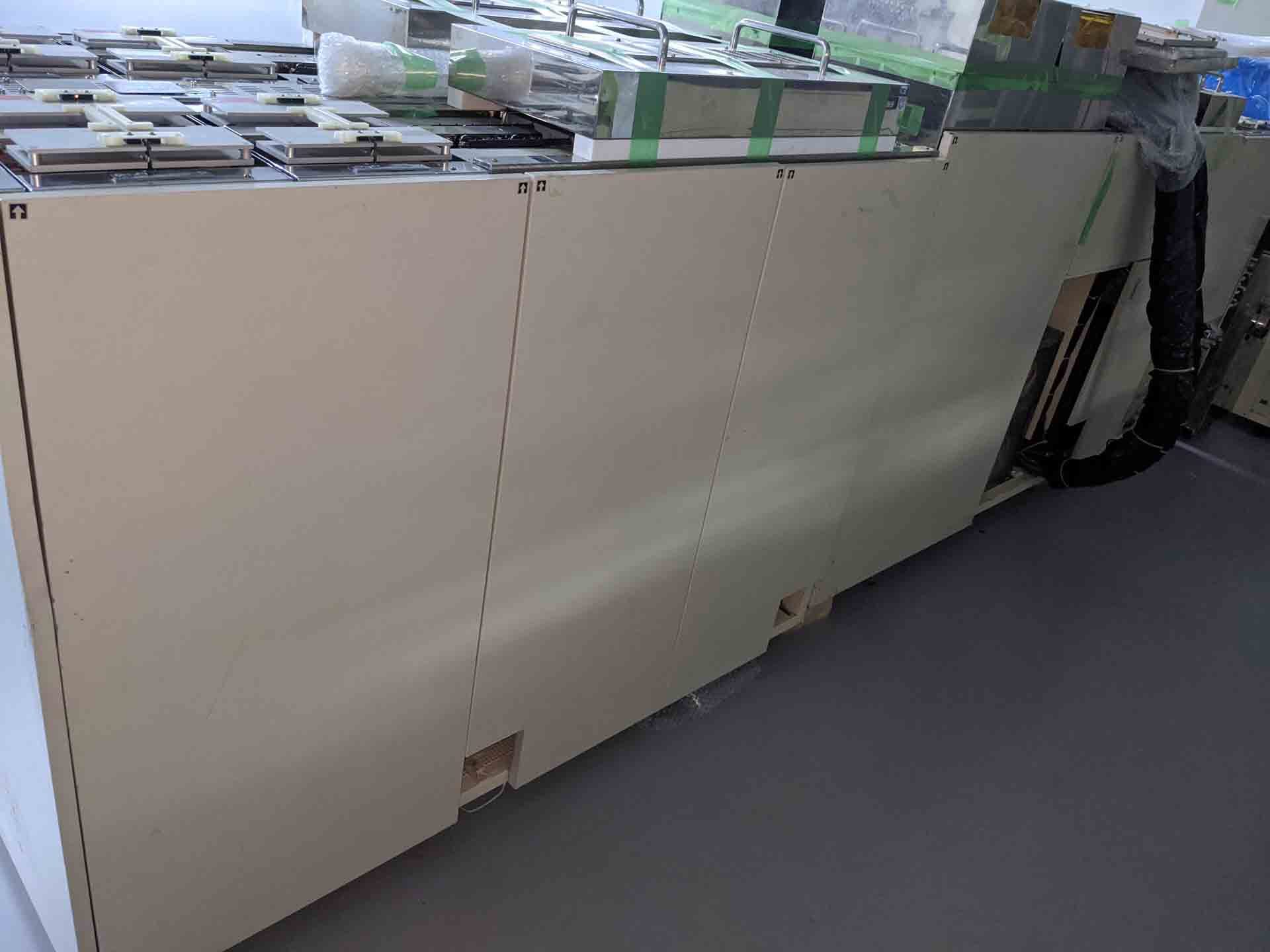

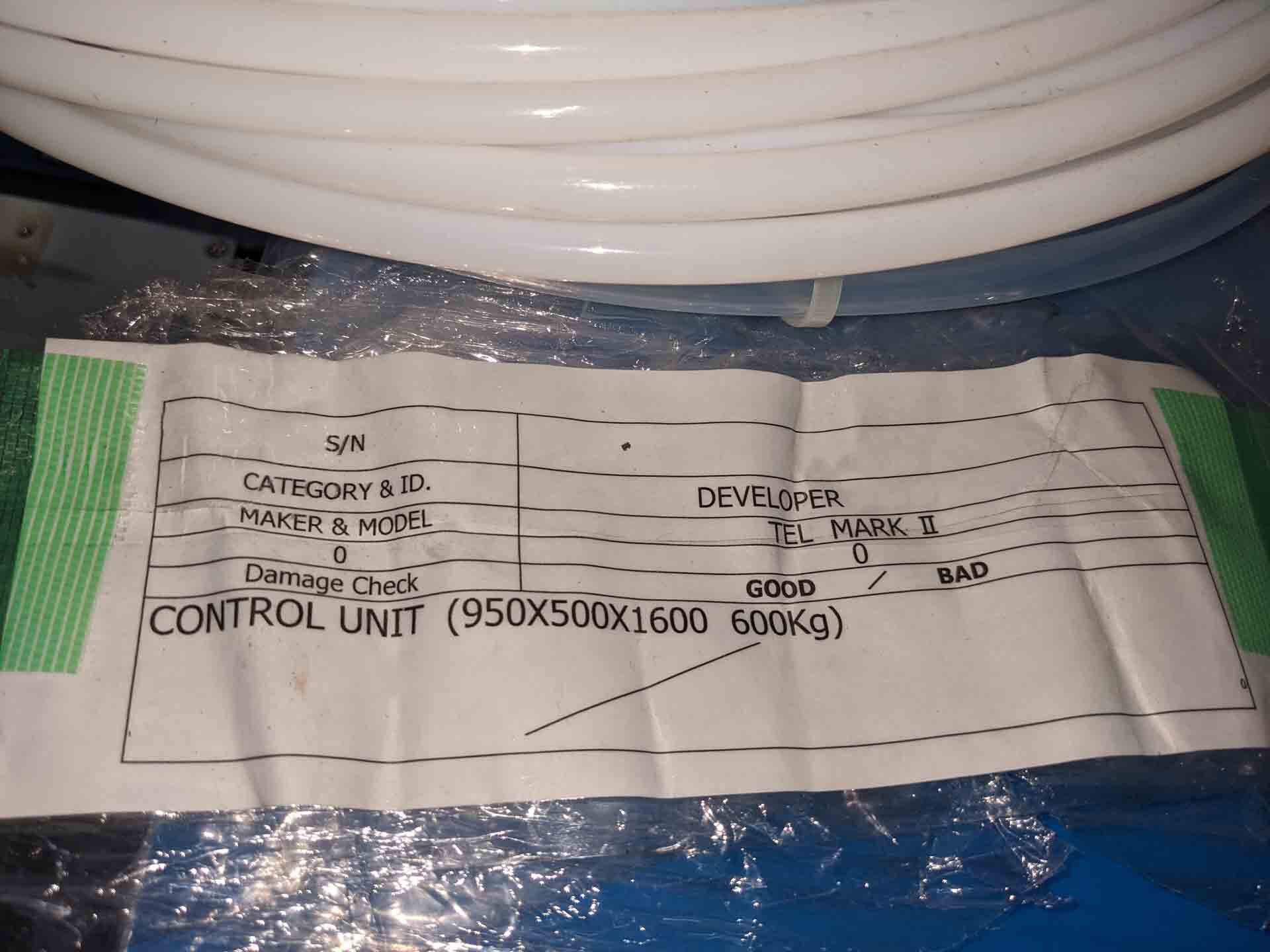


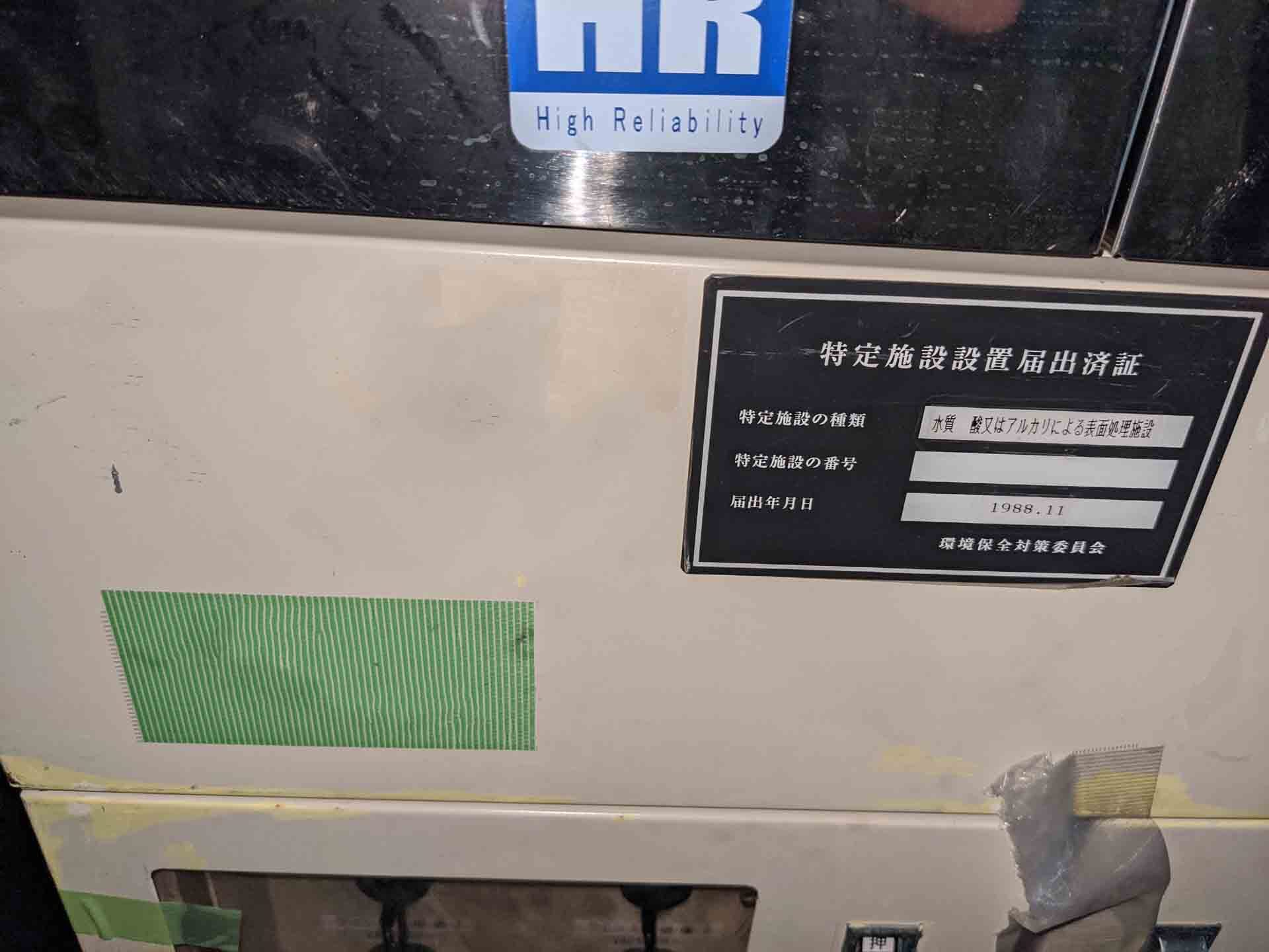

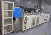
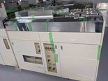
TEL / TOKYO ELECTRON MARK II is a photoresist equipment designed for the direct imaging of up to 4 inch wafers. The system's main components are its ultra-high-magnification projection optics, precision stage, and integrated PC and software. TEL MARK II's projection optics provides high-resolution imaging capabilities up to 814mm×1.2mm and magnification ratios up to 1.75. Its imaging lens is a multi-element zoom illuminated by an integrated halogen lamp. The dual optical cross-sections of the lens facilitate both low- and high-magnification imaging. In addition, the lens has a closed-loop automatic fast-zoom operation to quickly move between different magnification levels. The precision stage of TOKYO ELECTRON MARK II is designed for smooth operation and fast photoresist movement. The unit utilizes a piezo-driven motor to precisely move the wafer stage at up to 1mm per second. The stage is managed by an internal memory machine that stores up to 10,000 wafer coordinates and allows users to quickly move between them. The integrated PC and software of the tool can handle multiple image formats and is easily programmable for different wafer dimensions. It also provides for advanced splicing capabilities for seamlessly stitching together images from different sections of the wafer. The software also offers advanced functions such as programmable exposure sequencing, autofocus, and adjustable imaging parameters. MARK II is ideal for efficient, accurate photoresist imaging of up to 4-inch wafers. Its ultra-high magnification optics and precision stage provide the accuracy and resolution required while its PC and software provide a variety of advanced imaging capabilities.
There are no reviews yet
