Used TEL / TOKYO ELECTRON MARK II #293662824 for sale
URL successfully copied!

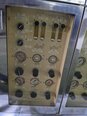
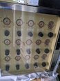
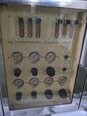
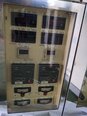
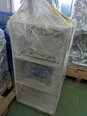
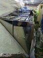
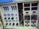




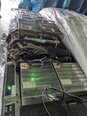
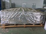
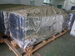




Tap to zoom
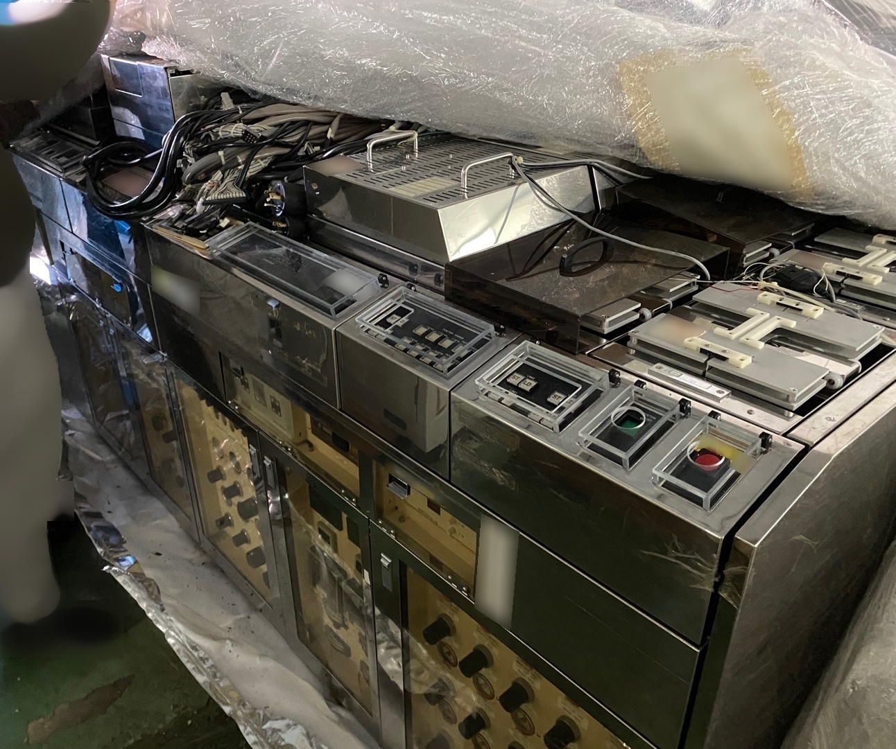

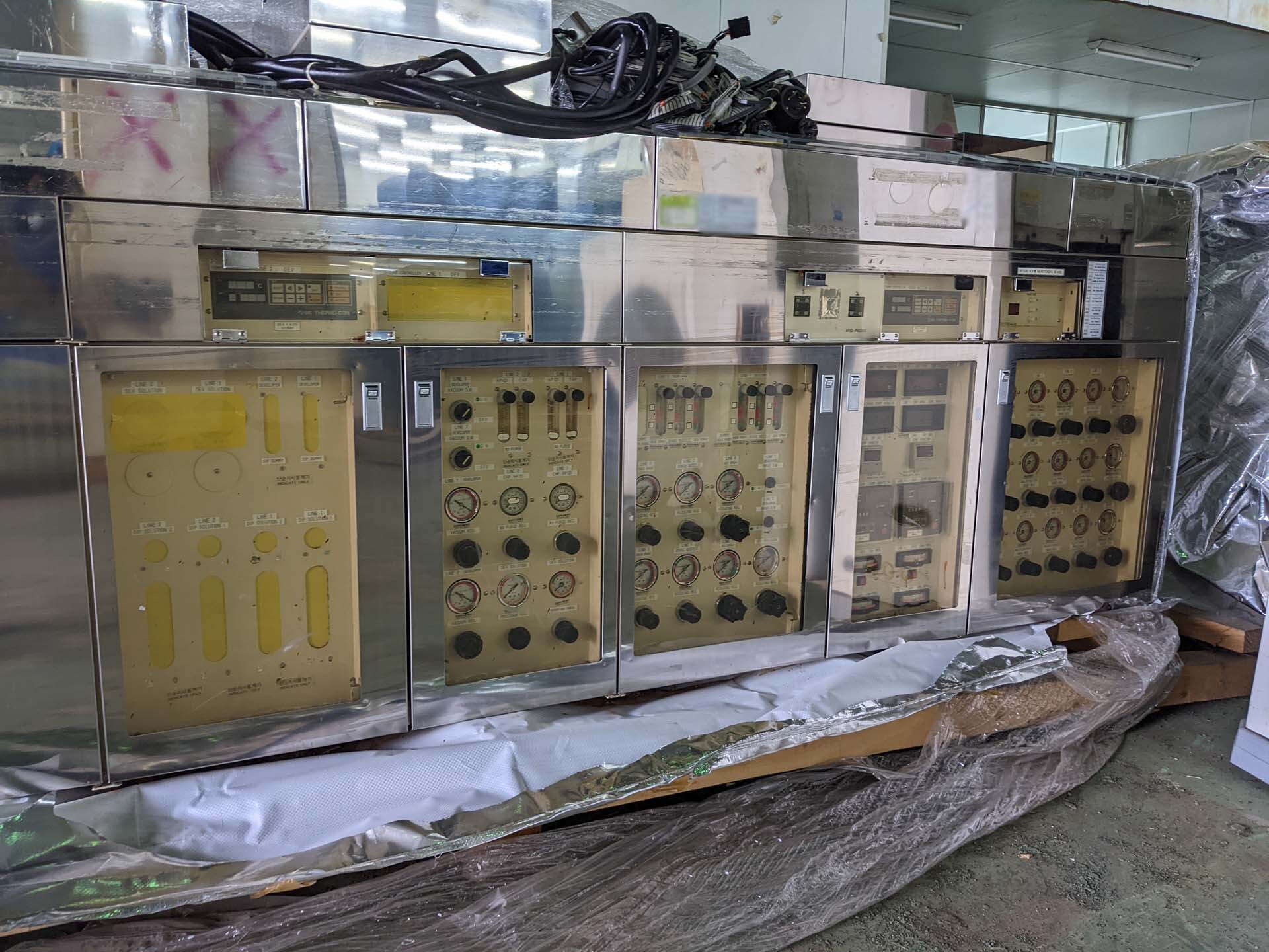
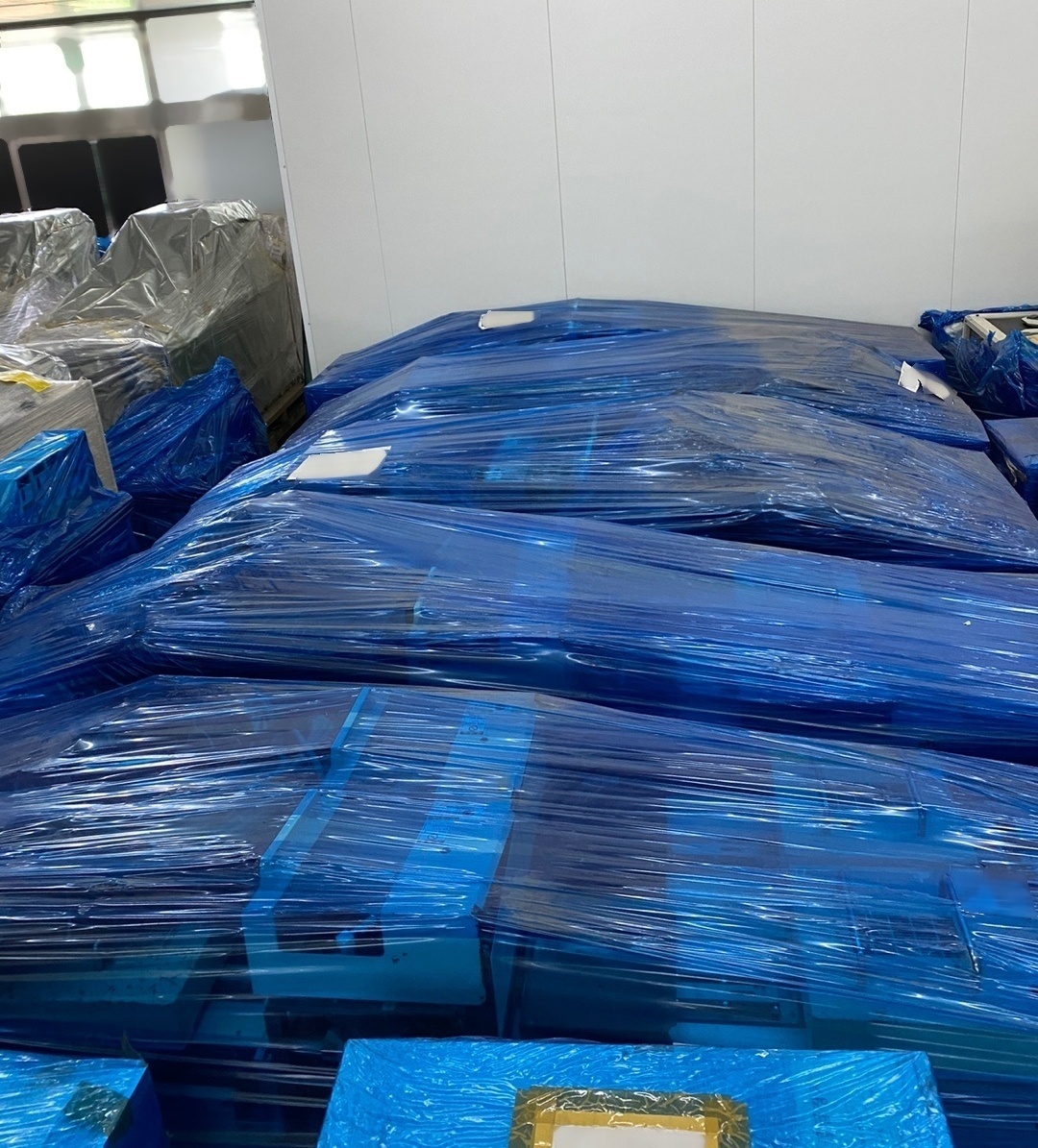
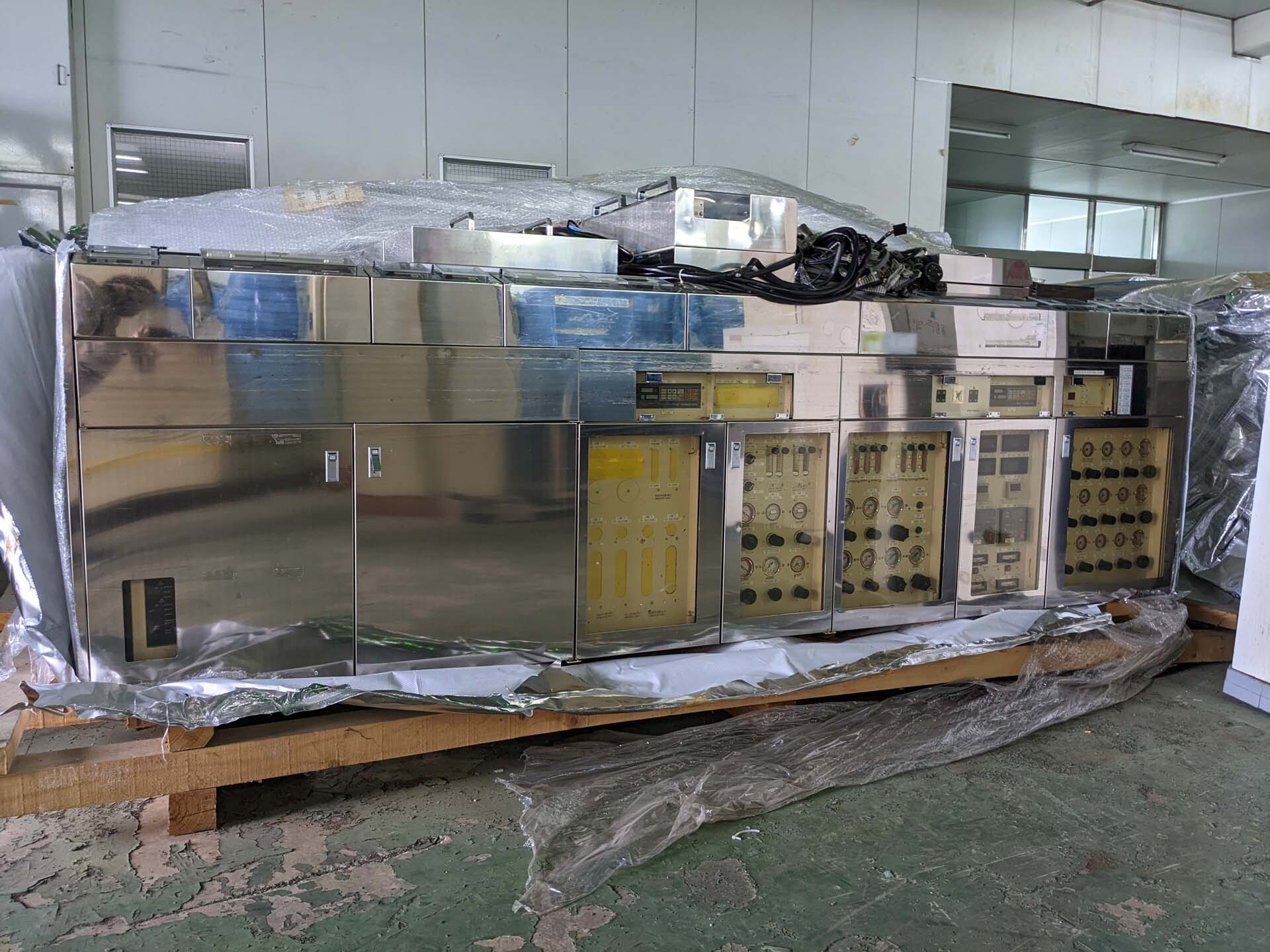
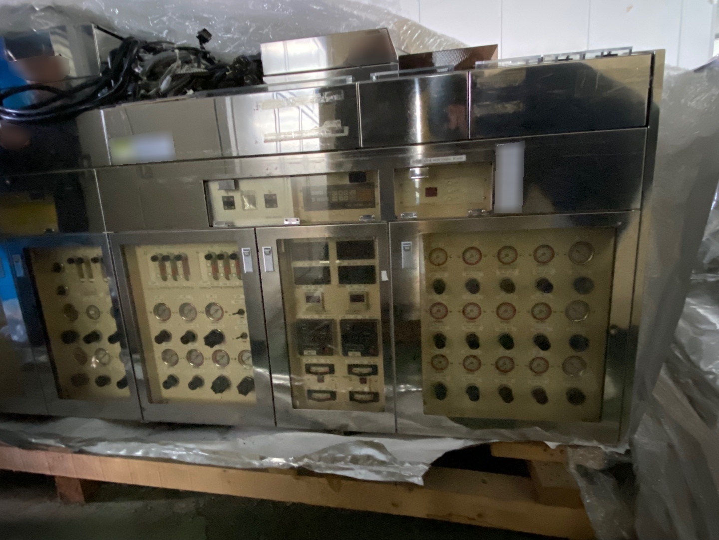
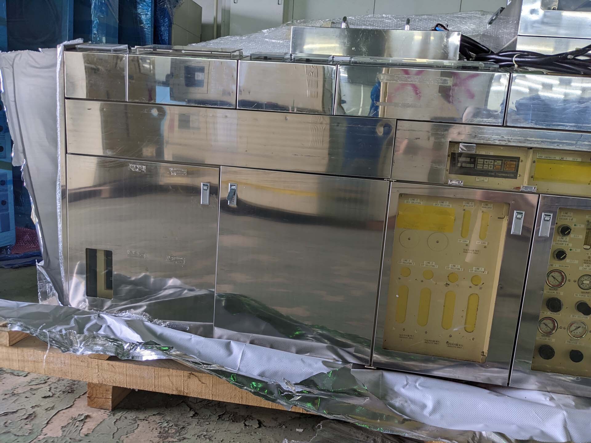
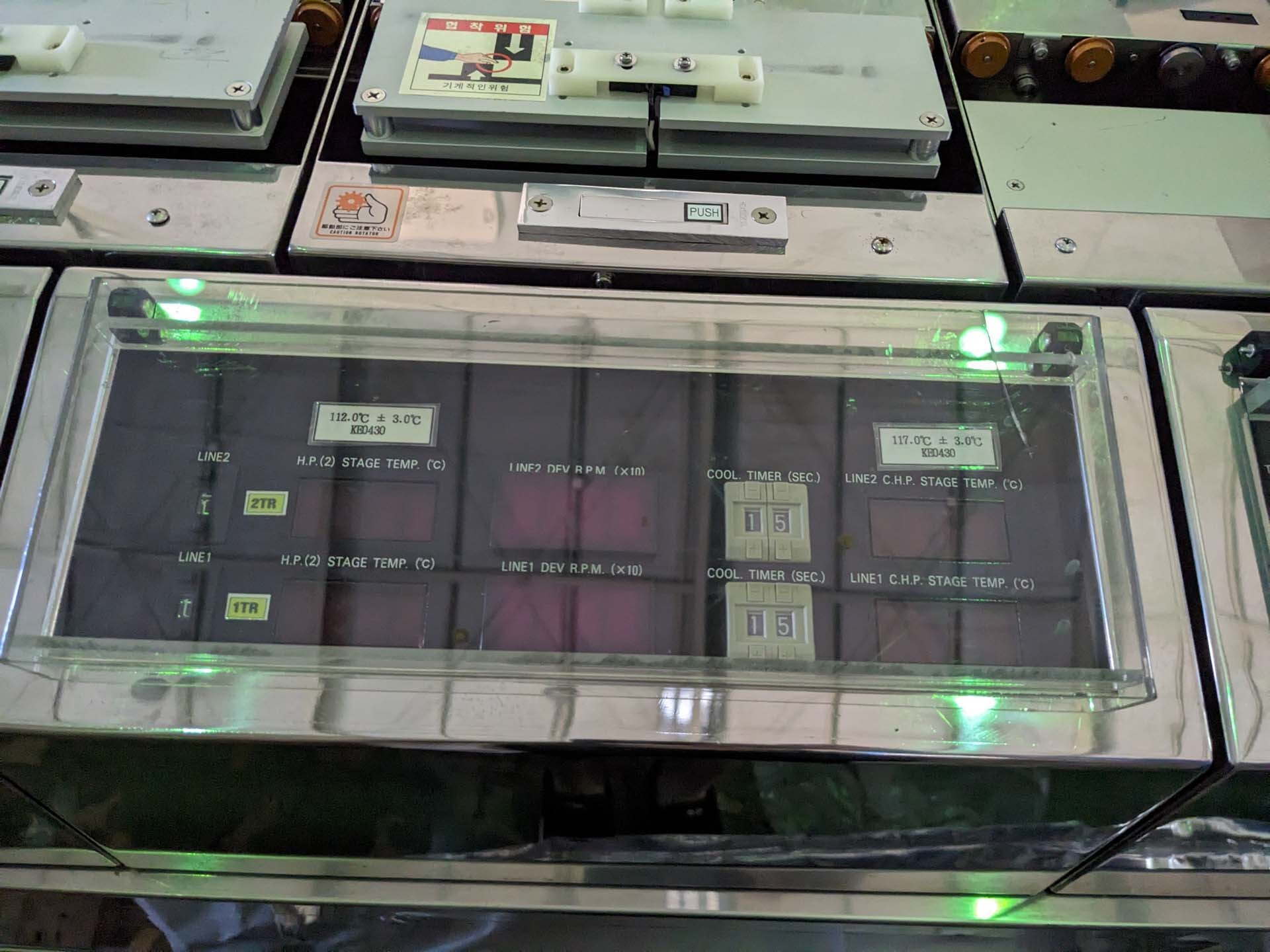
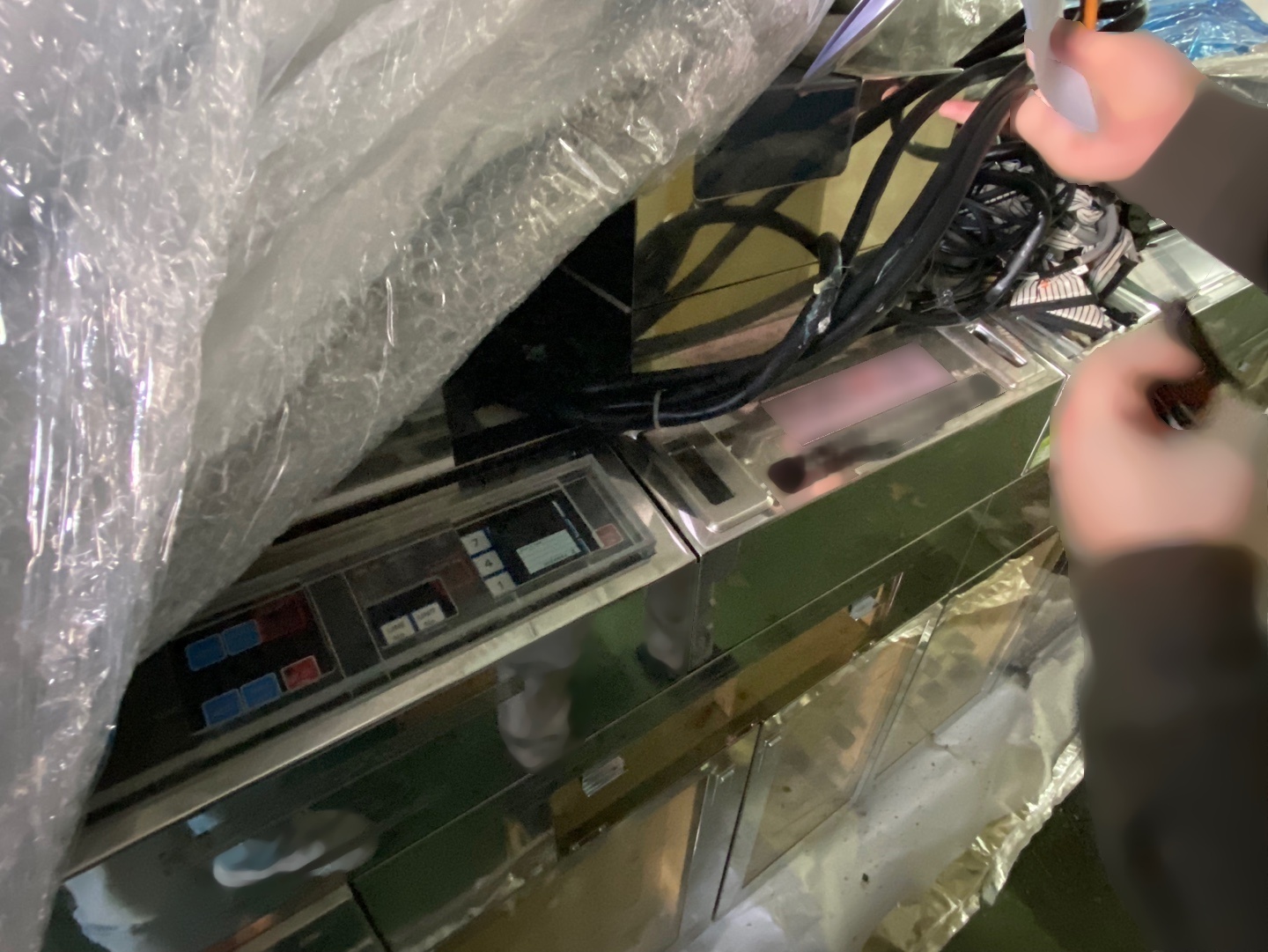
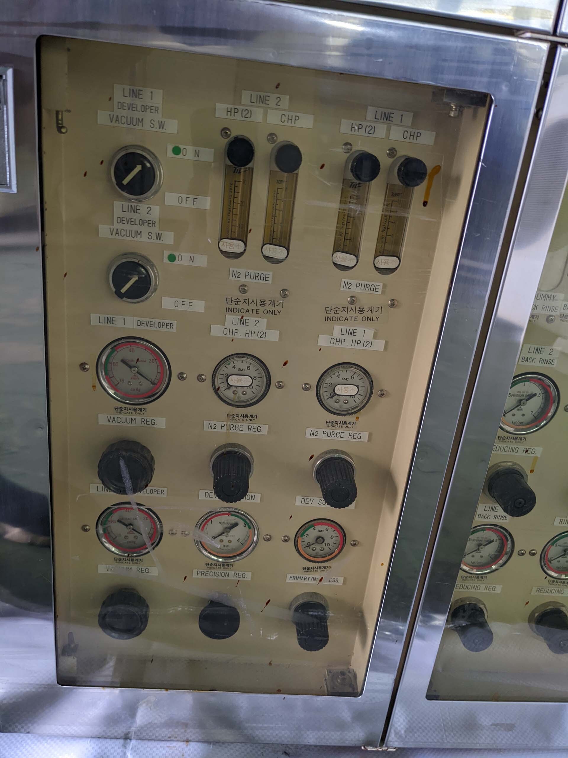
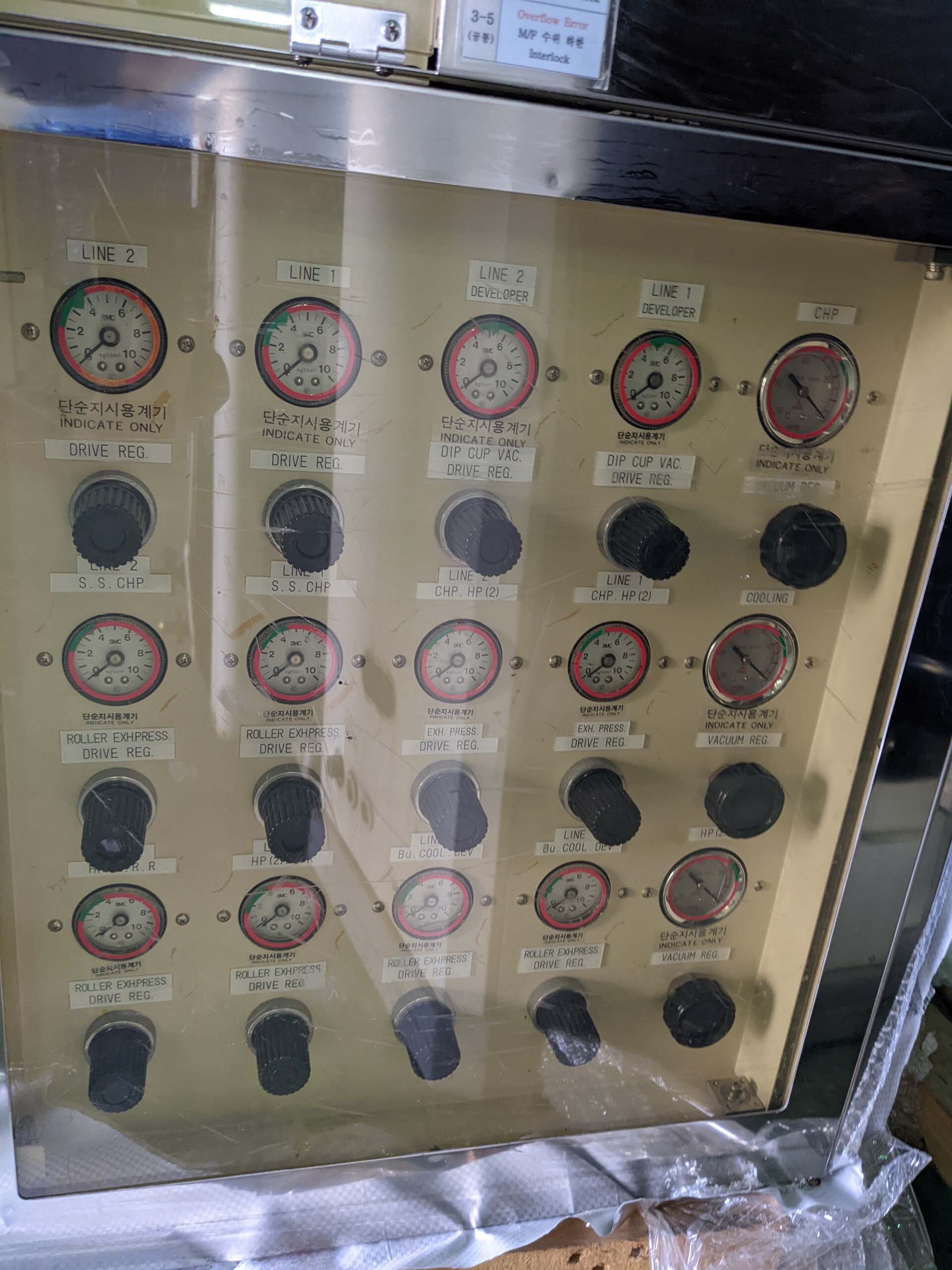
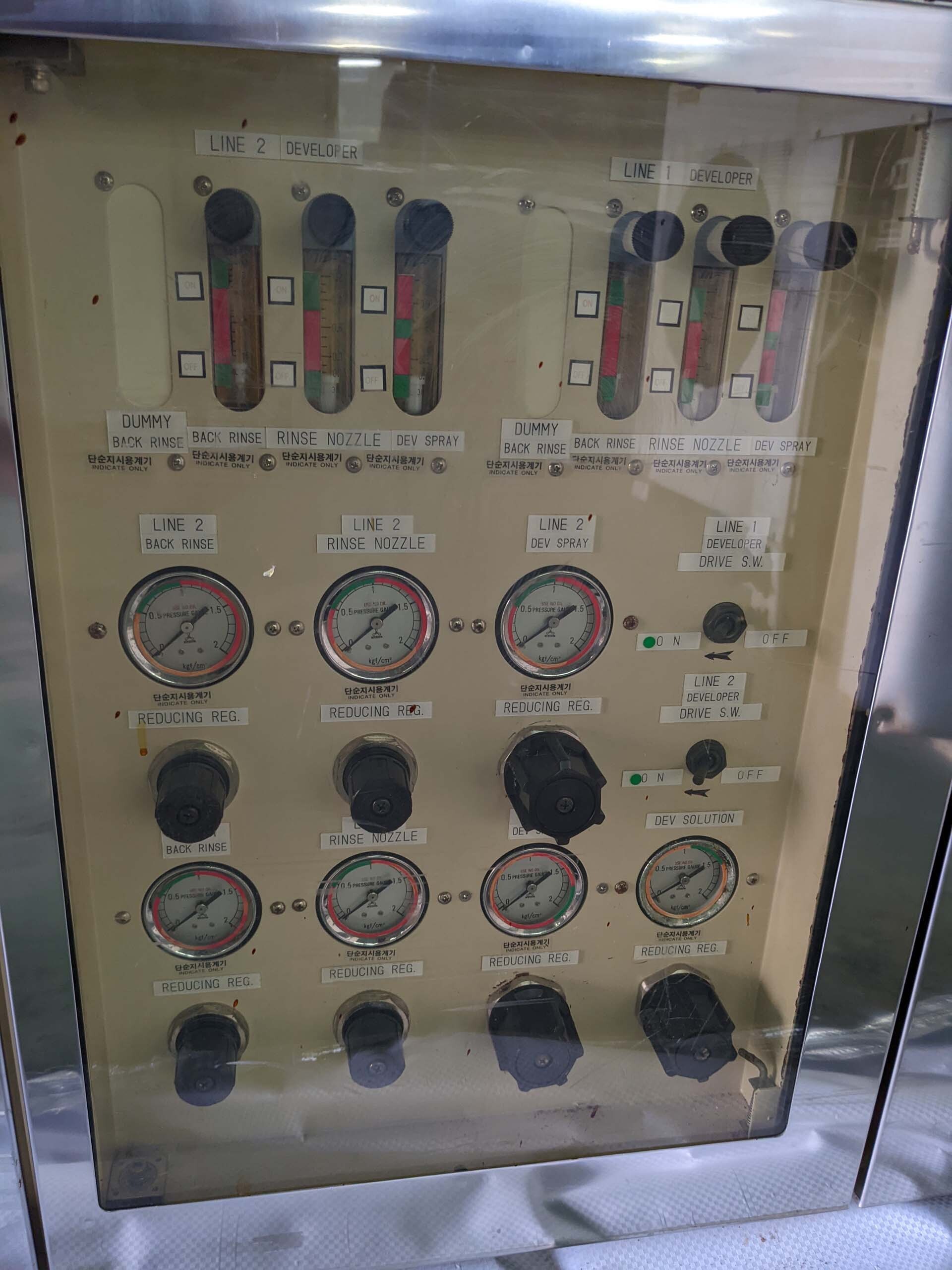
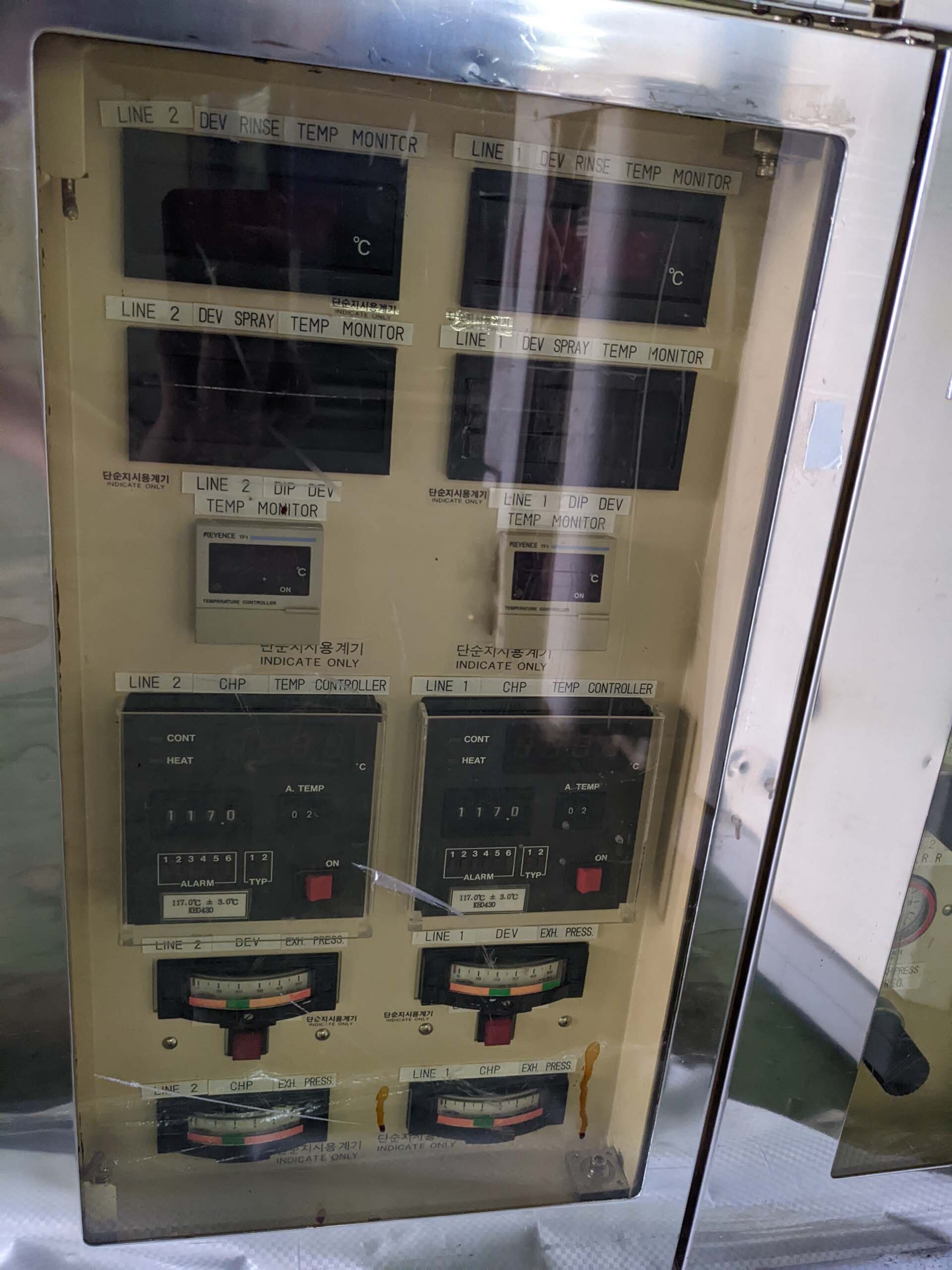
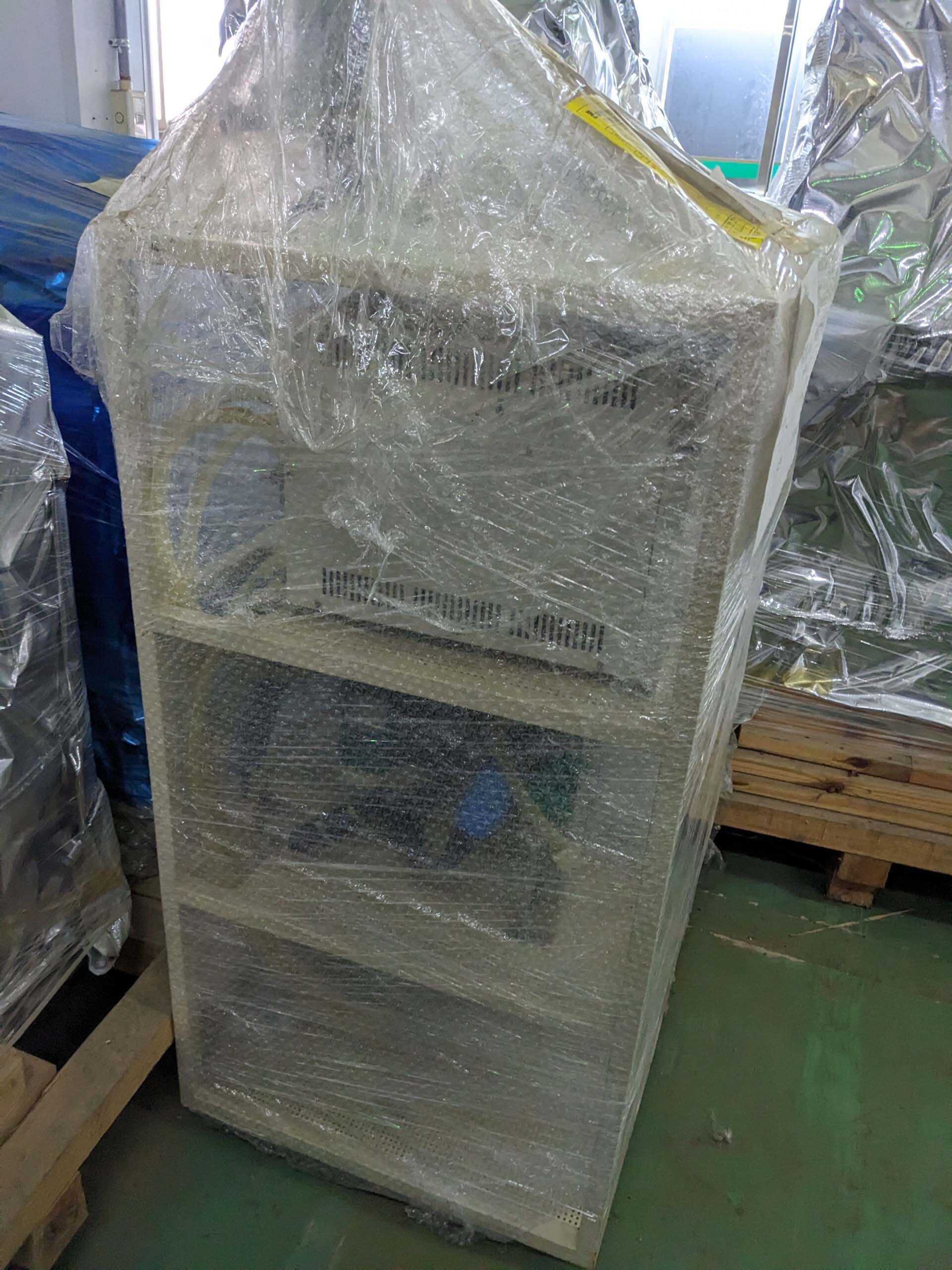
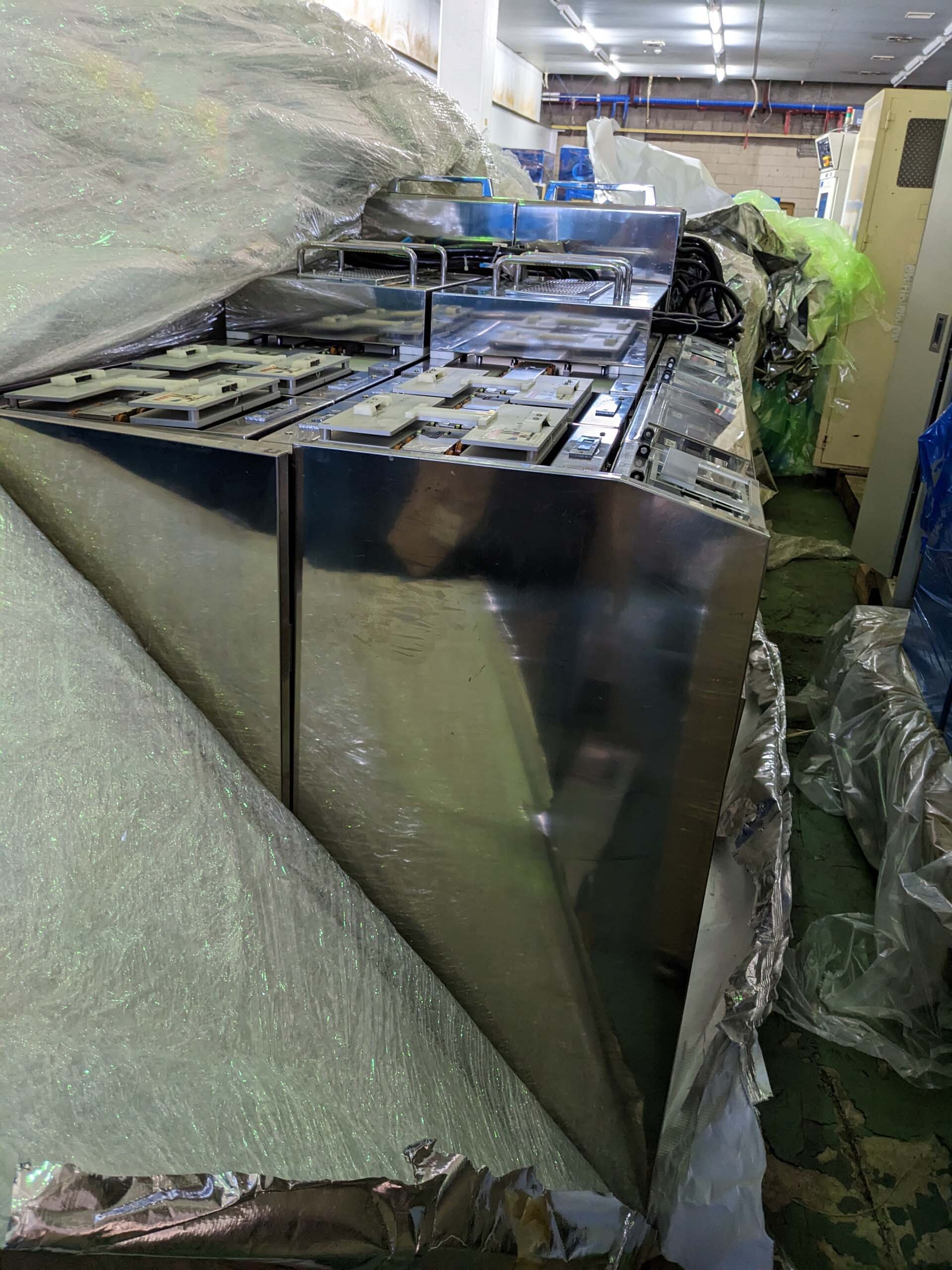
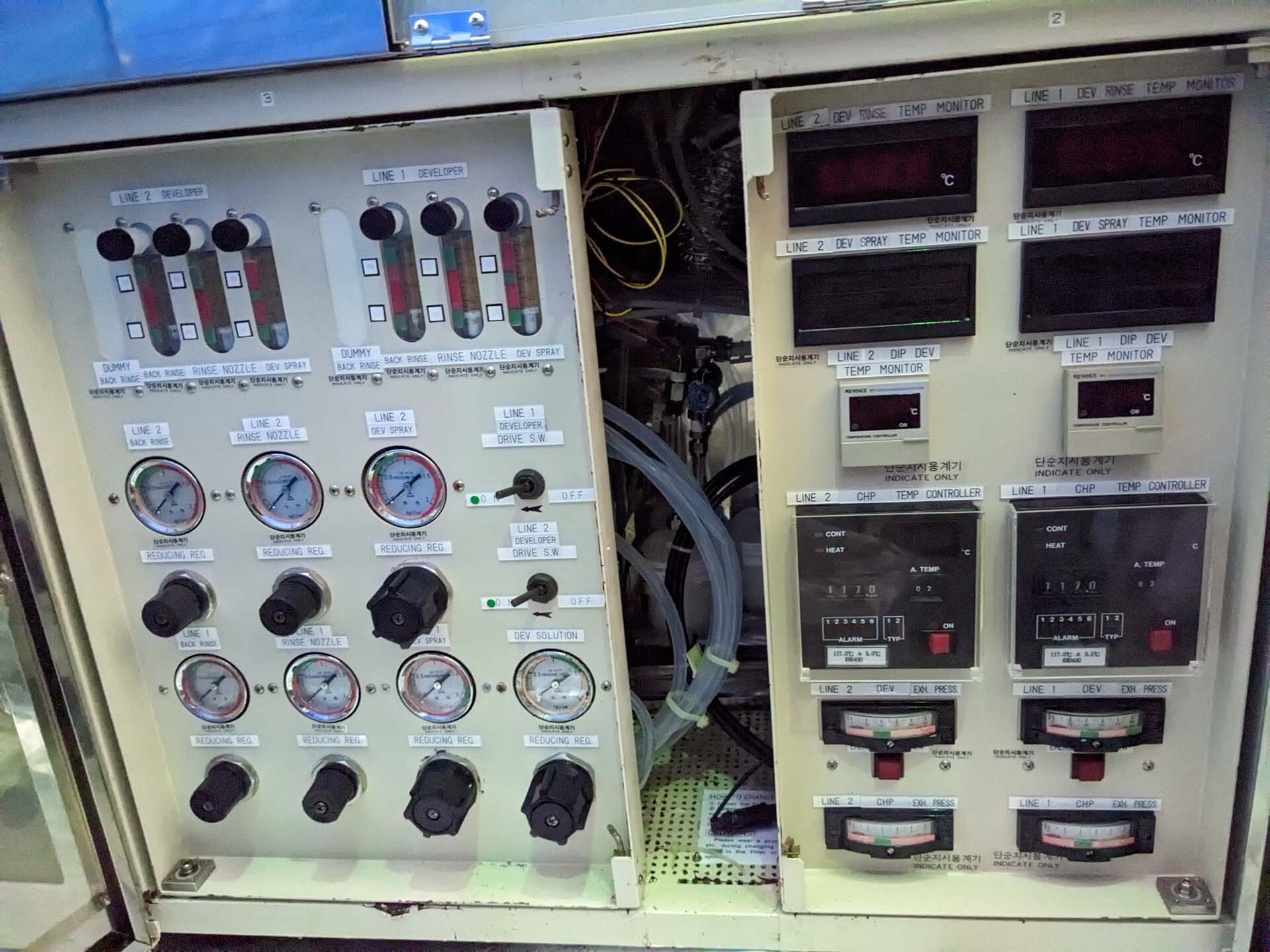
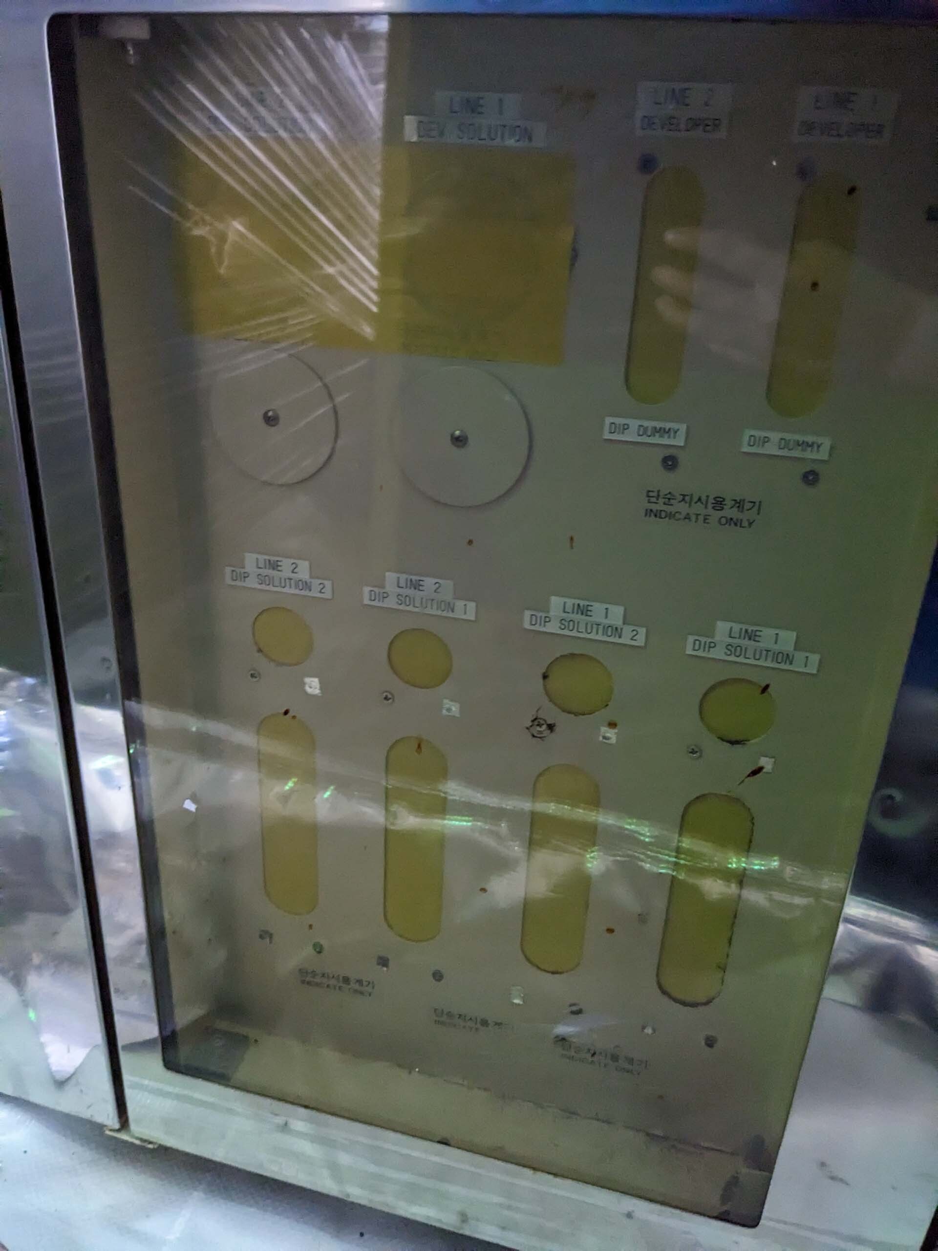
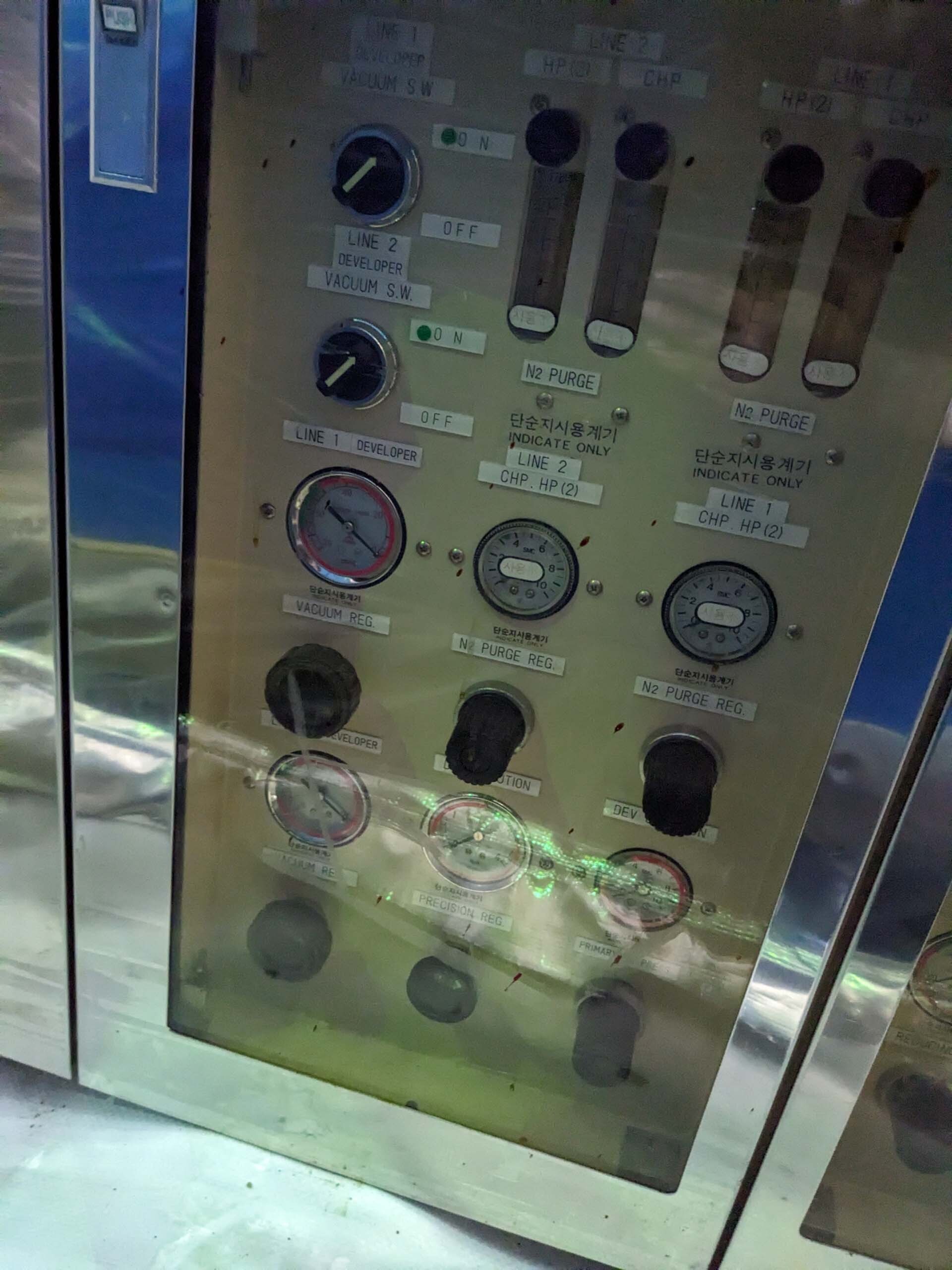
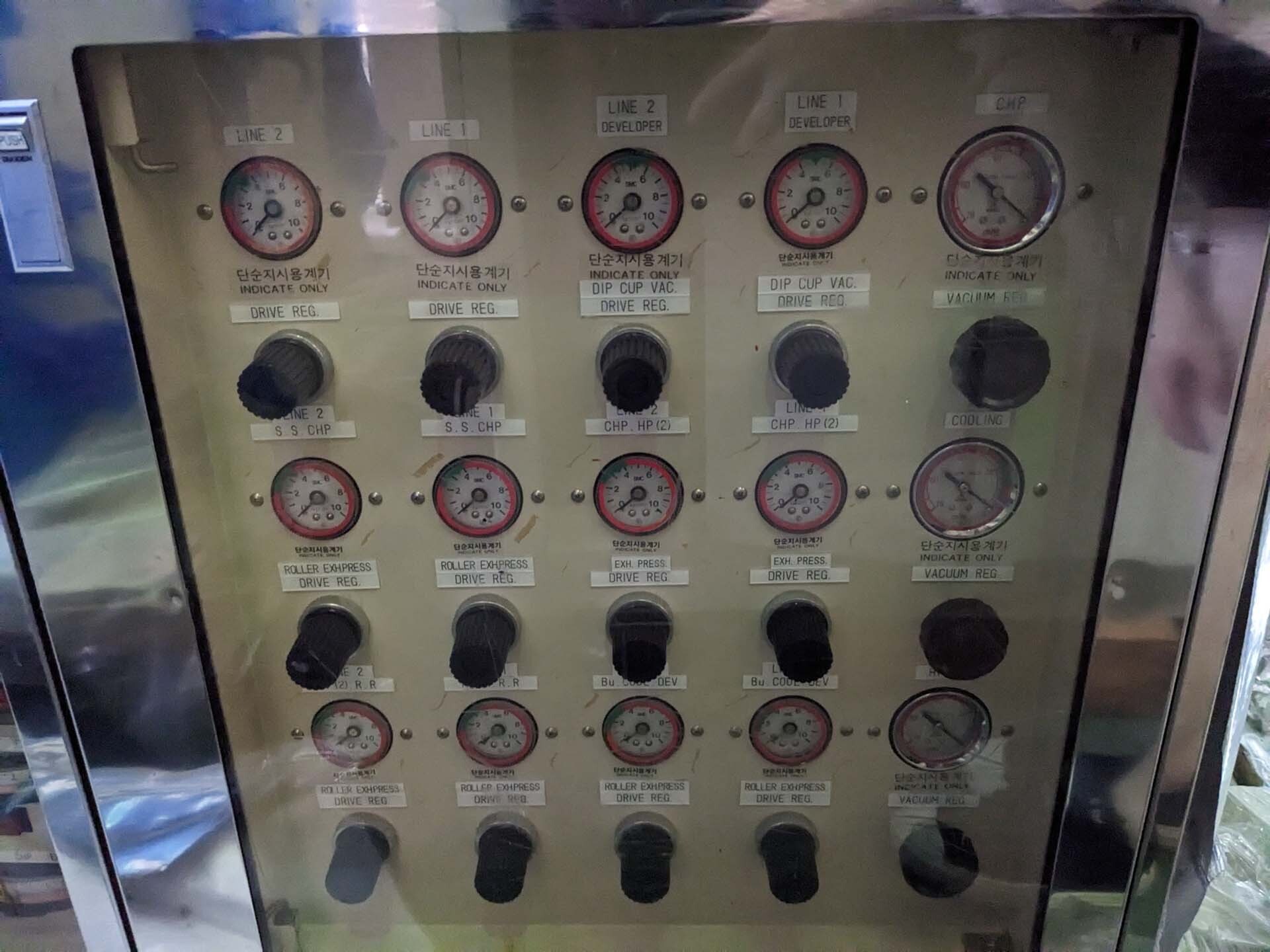
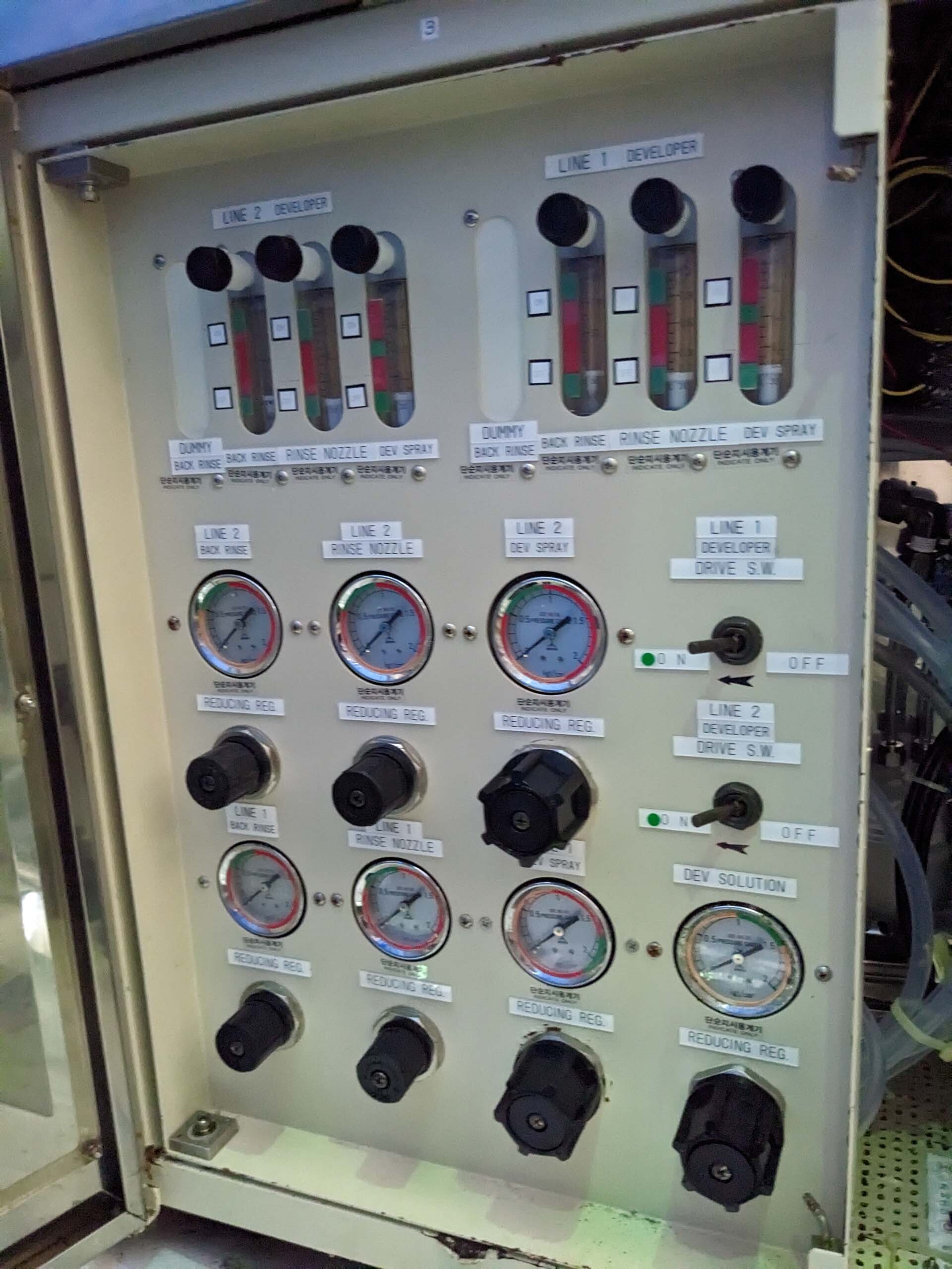
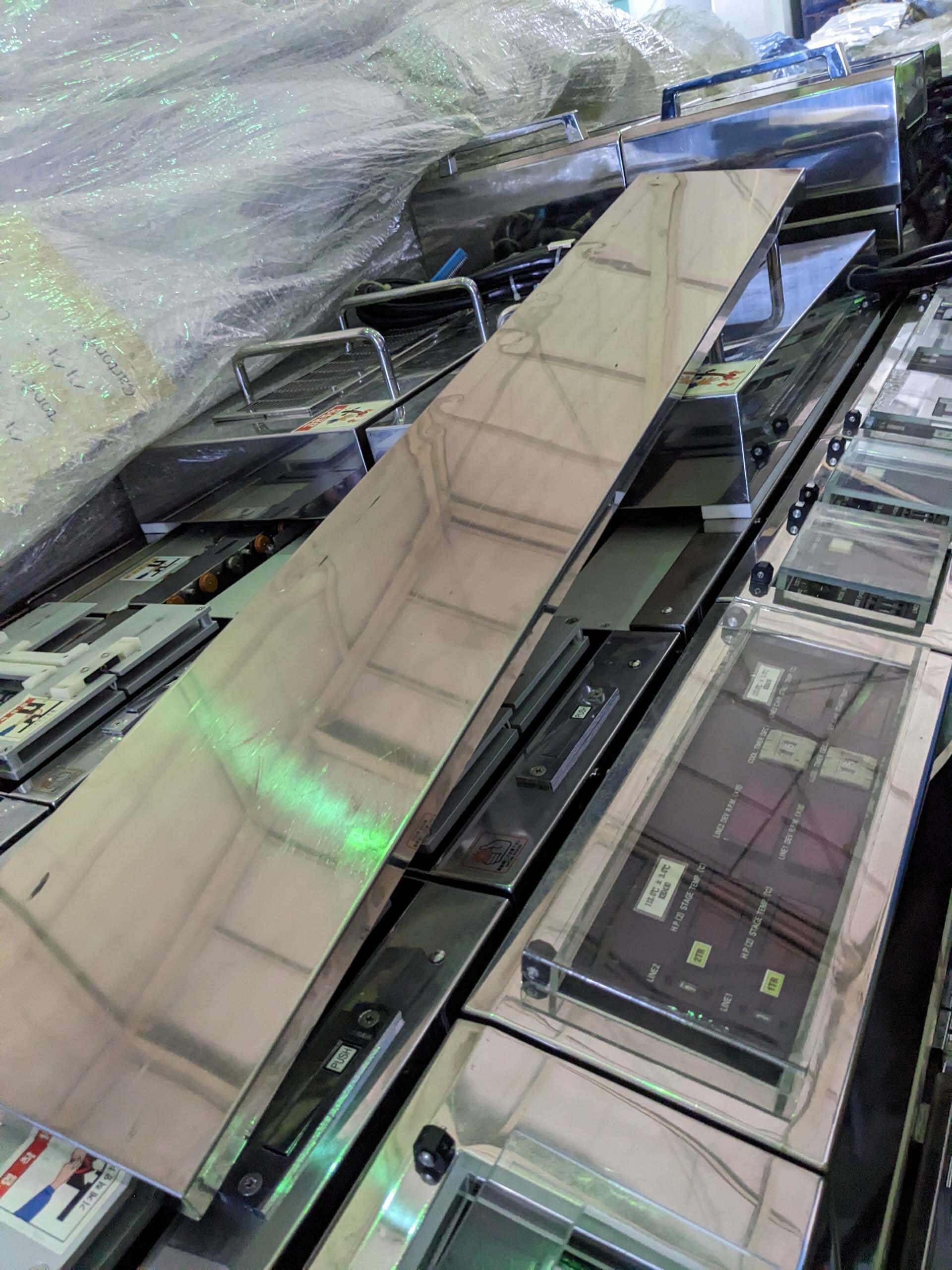
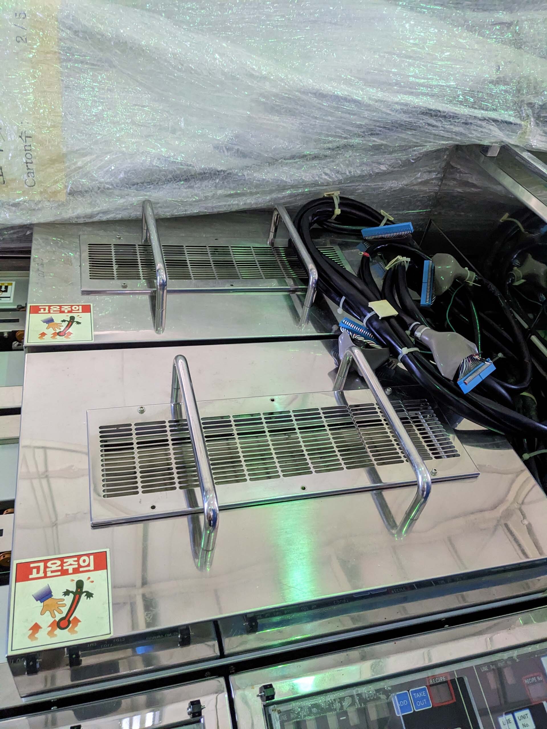
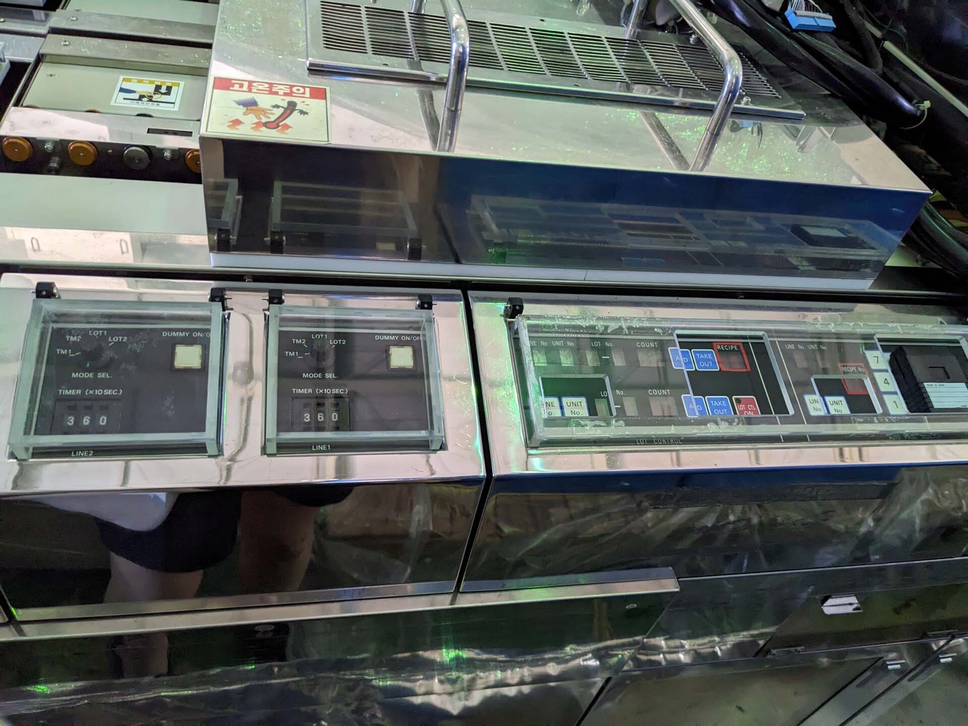
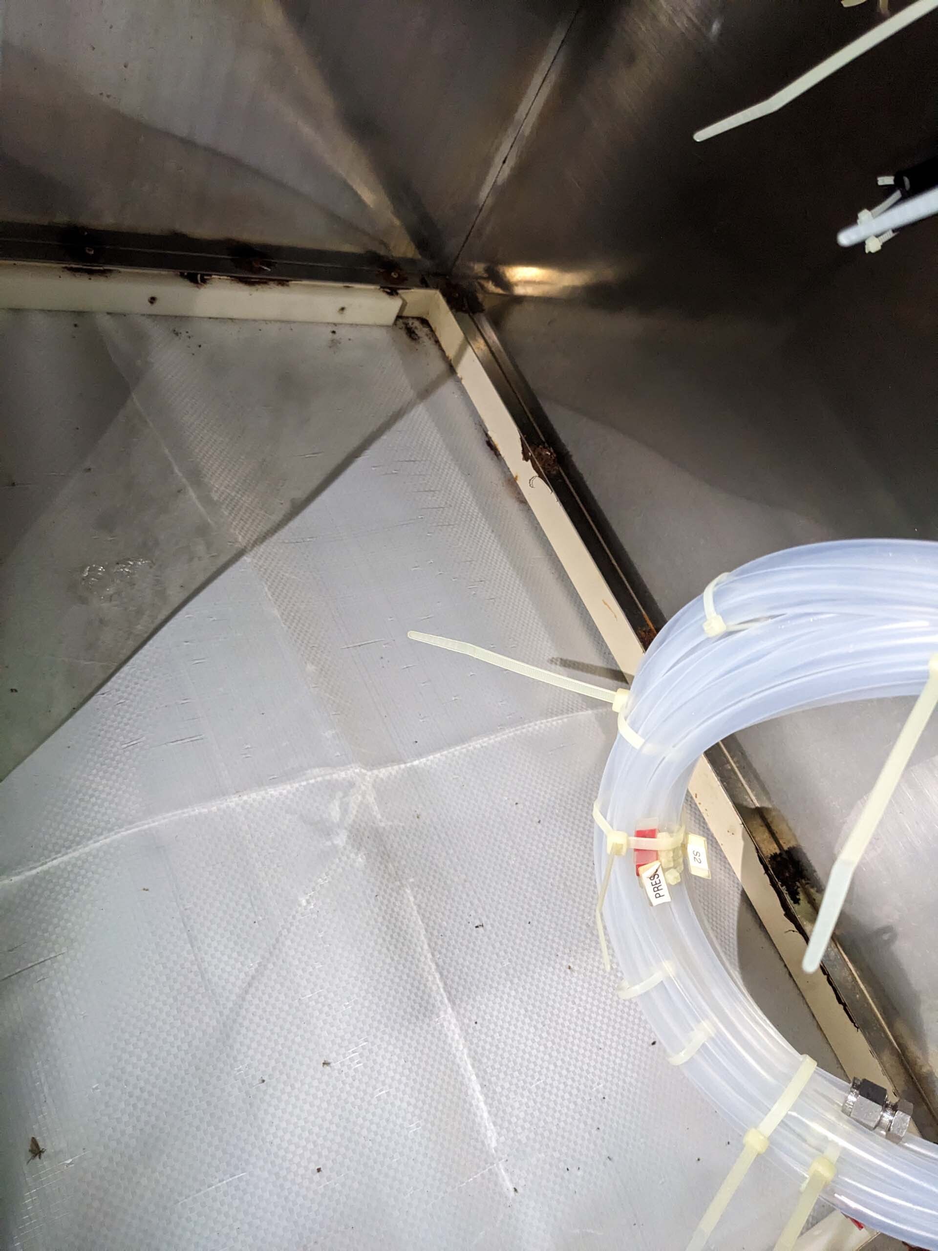
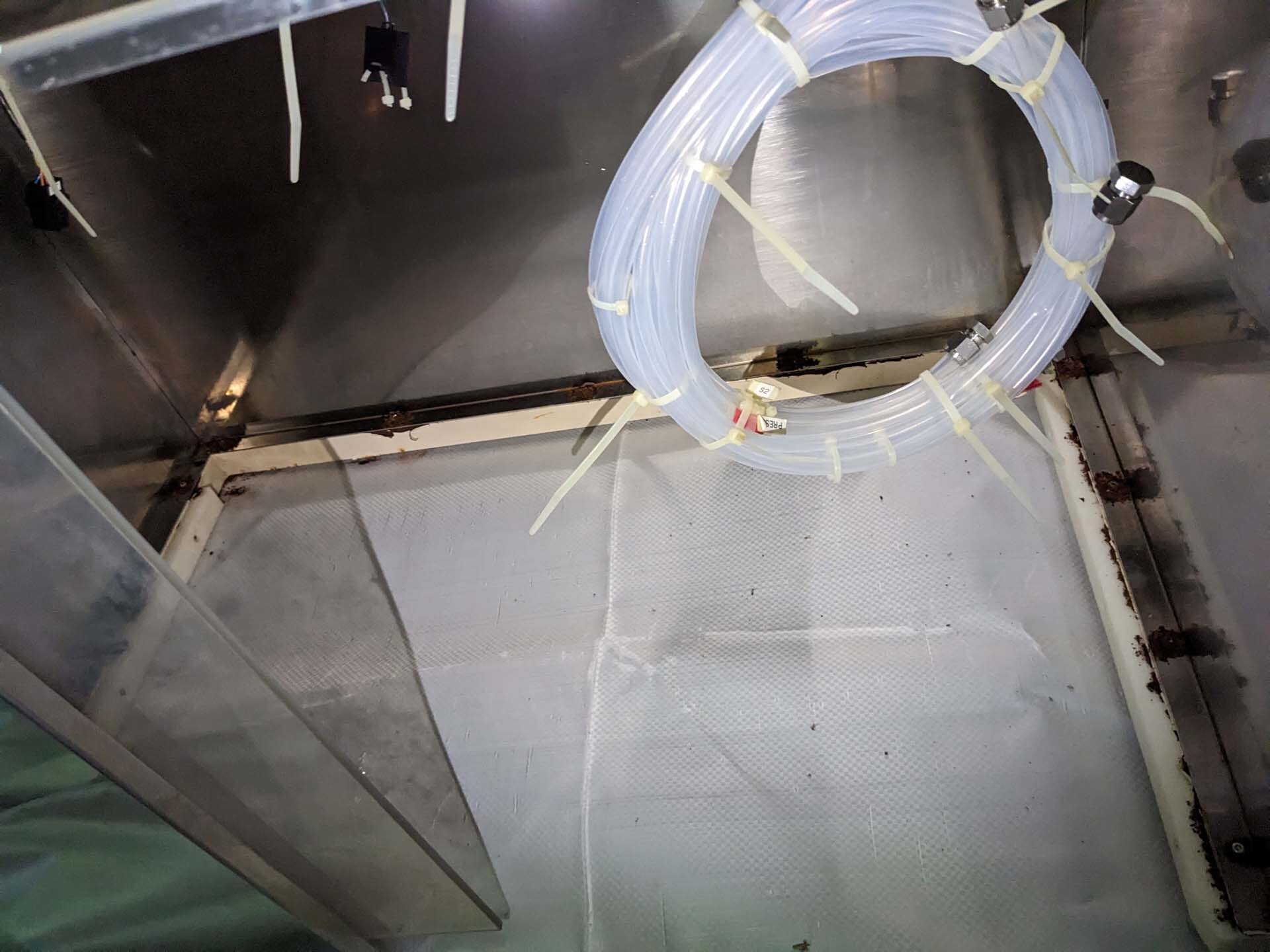
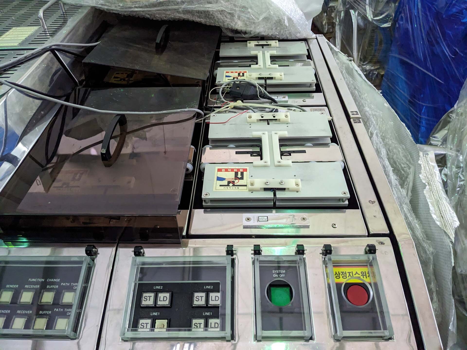
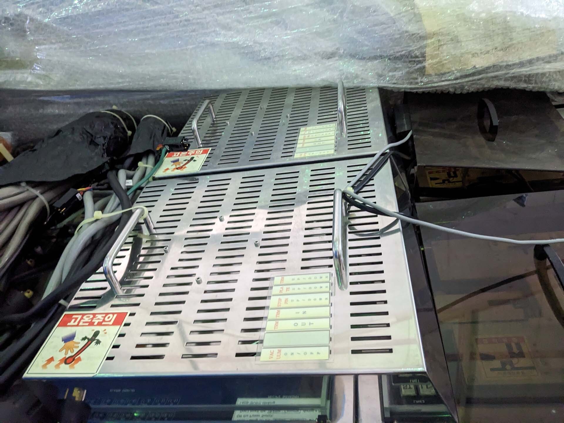
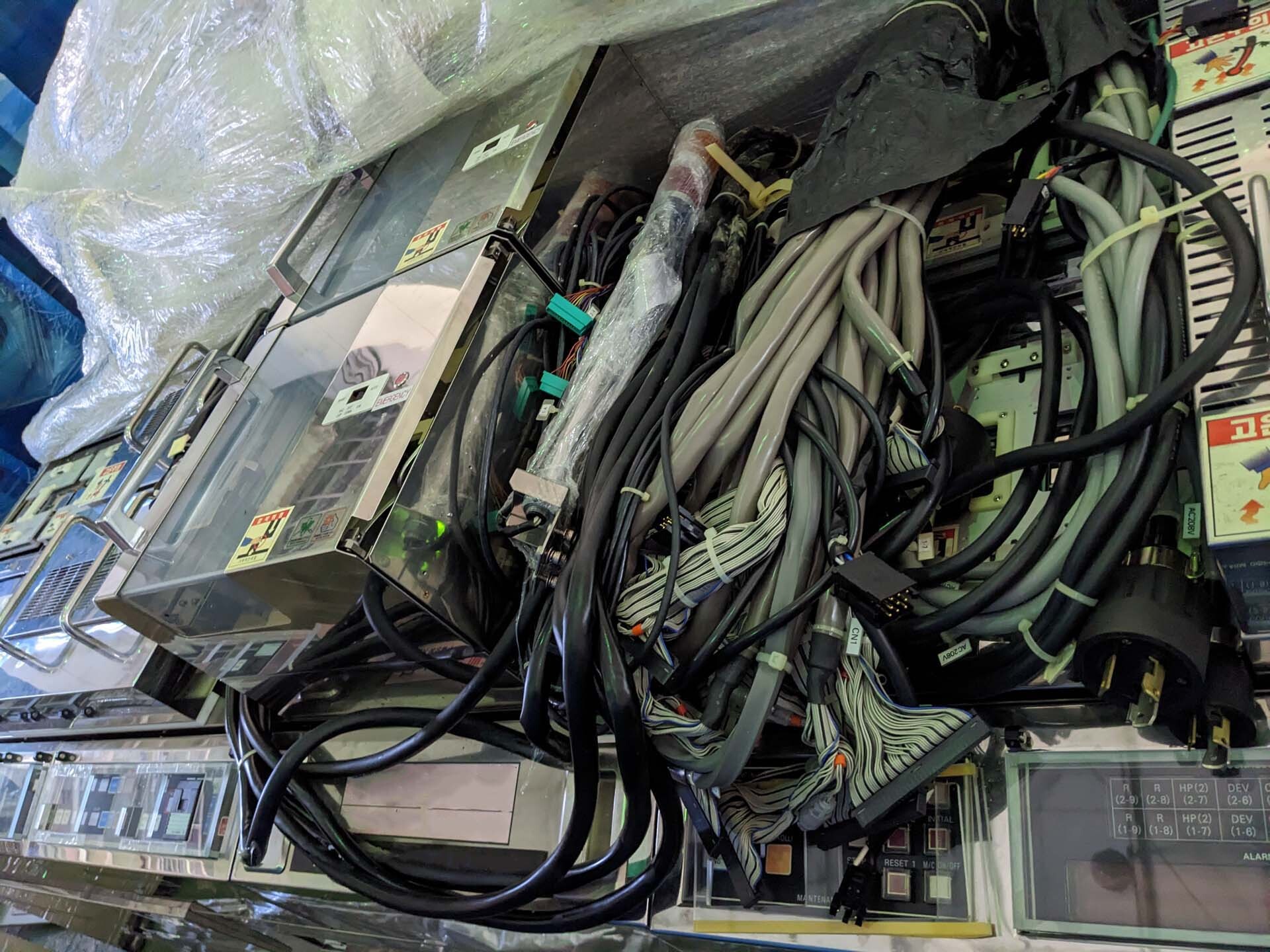
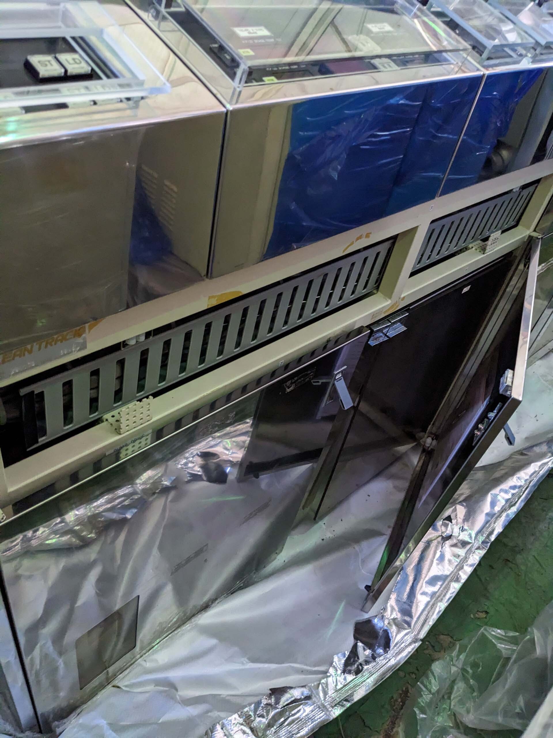
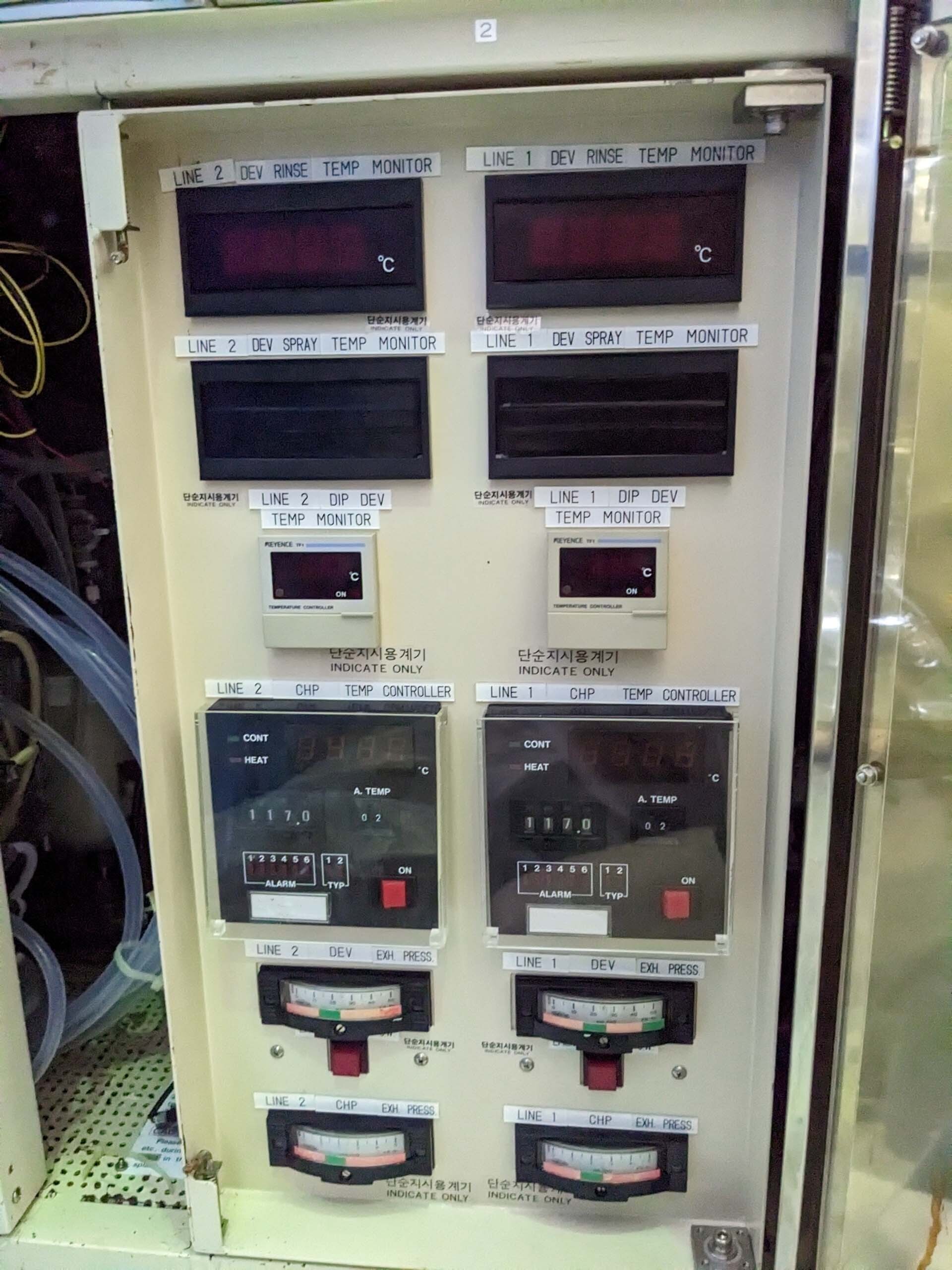
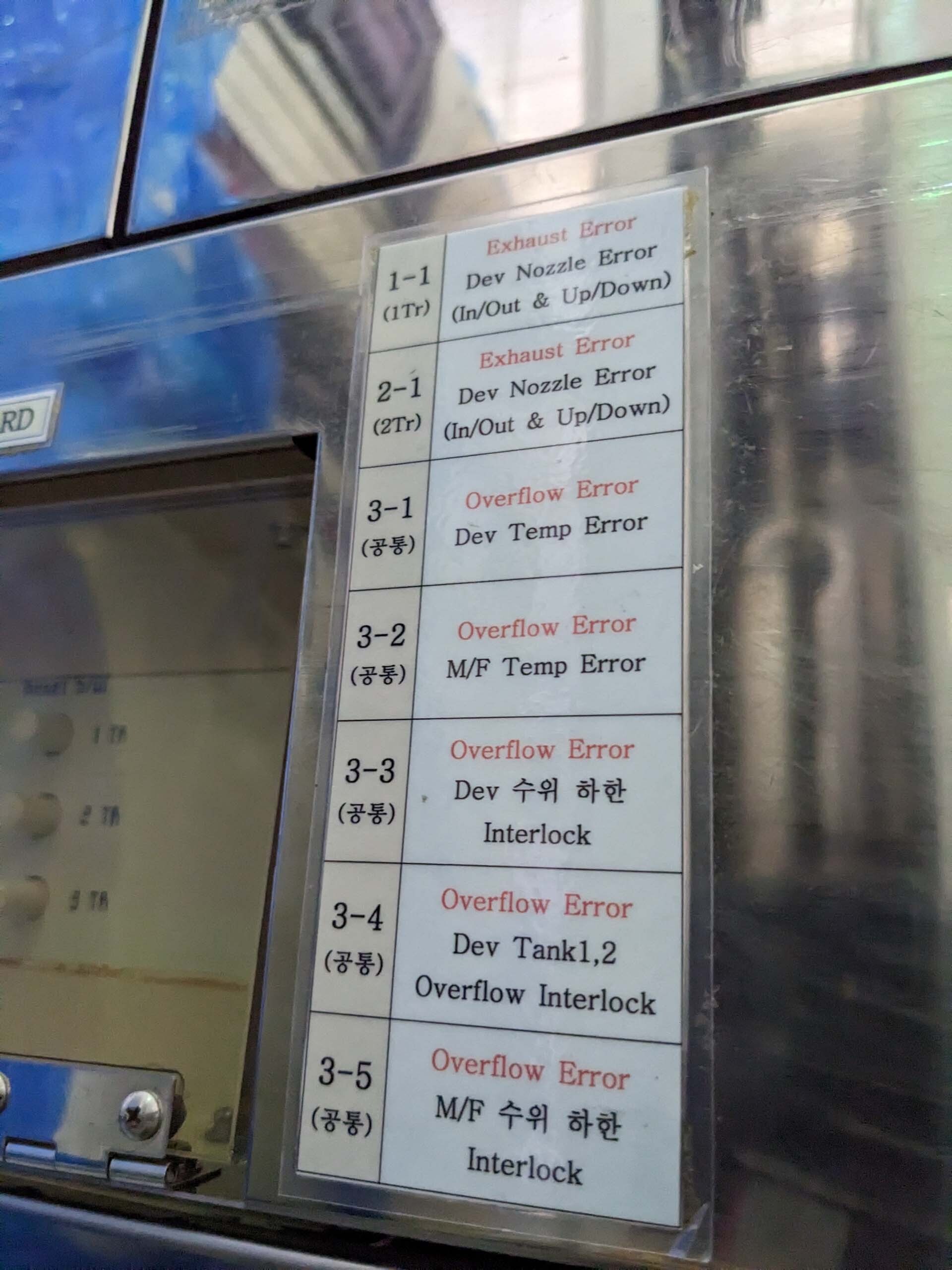
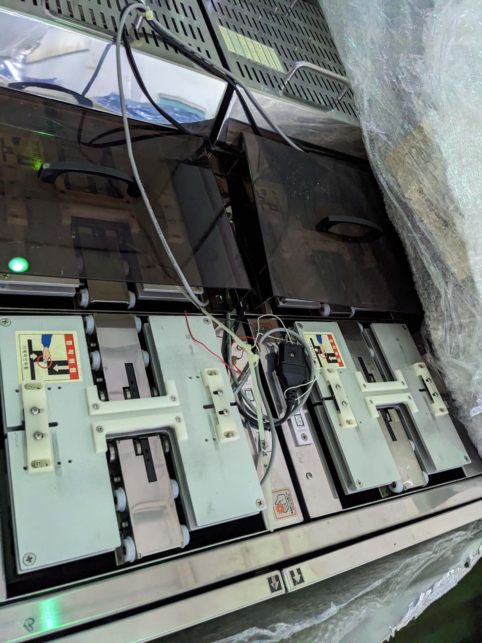
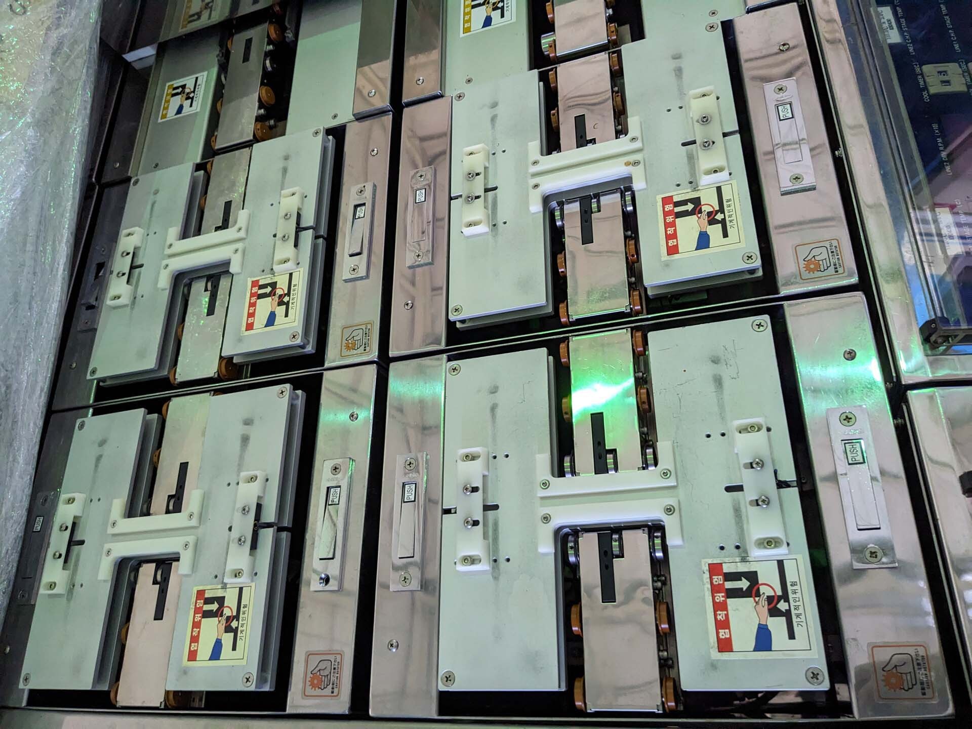
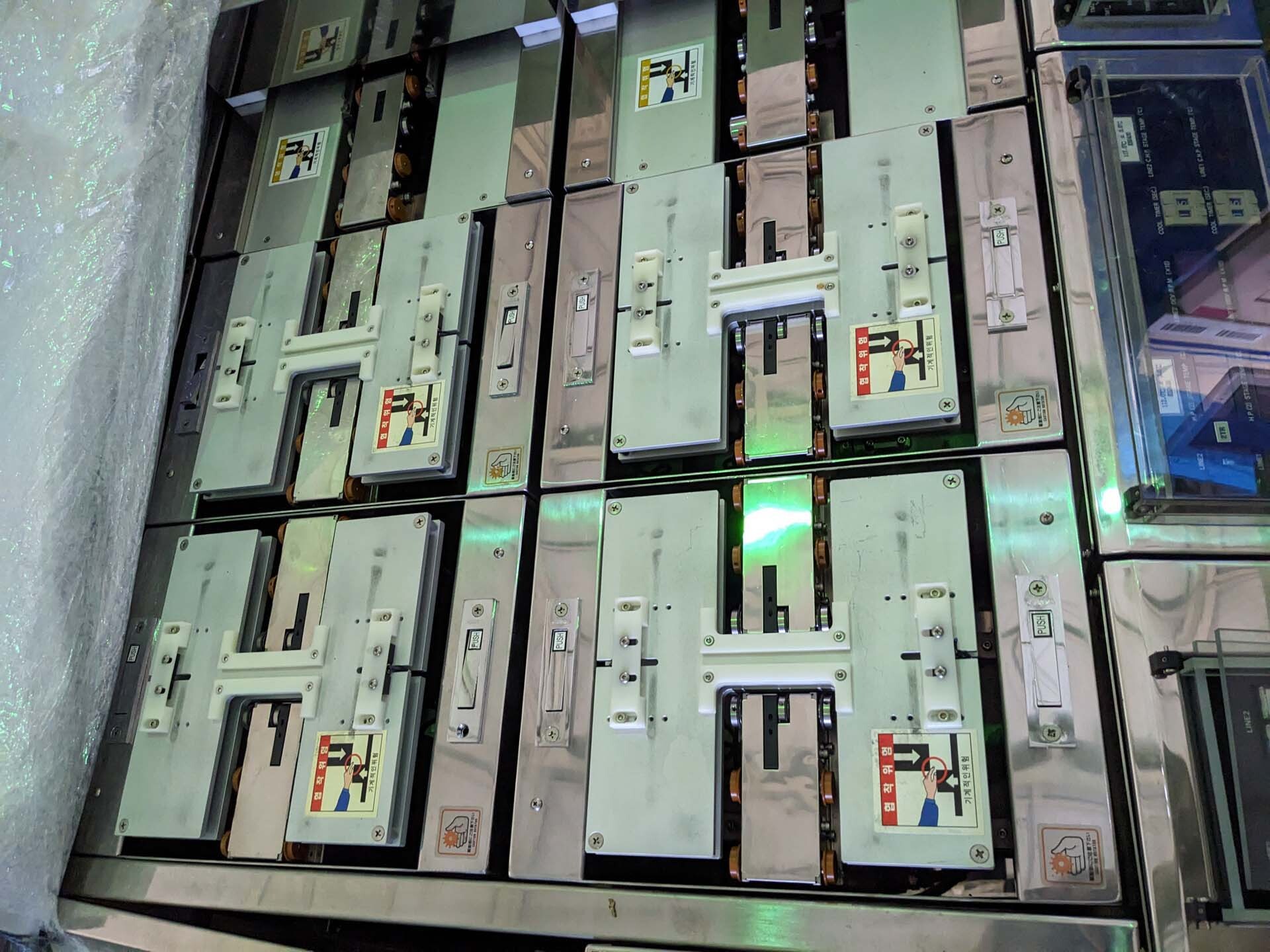
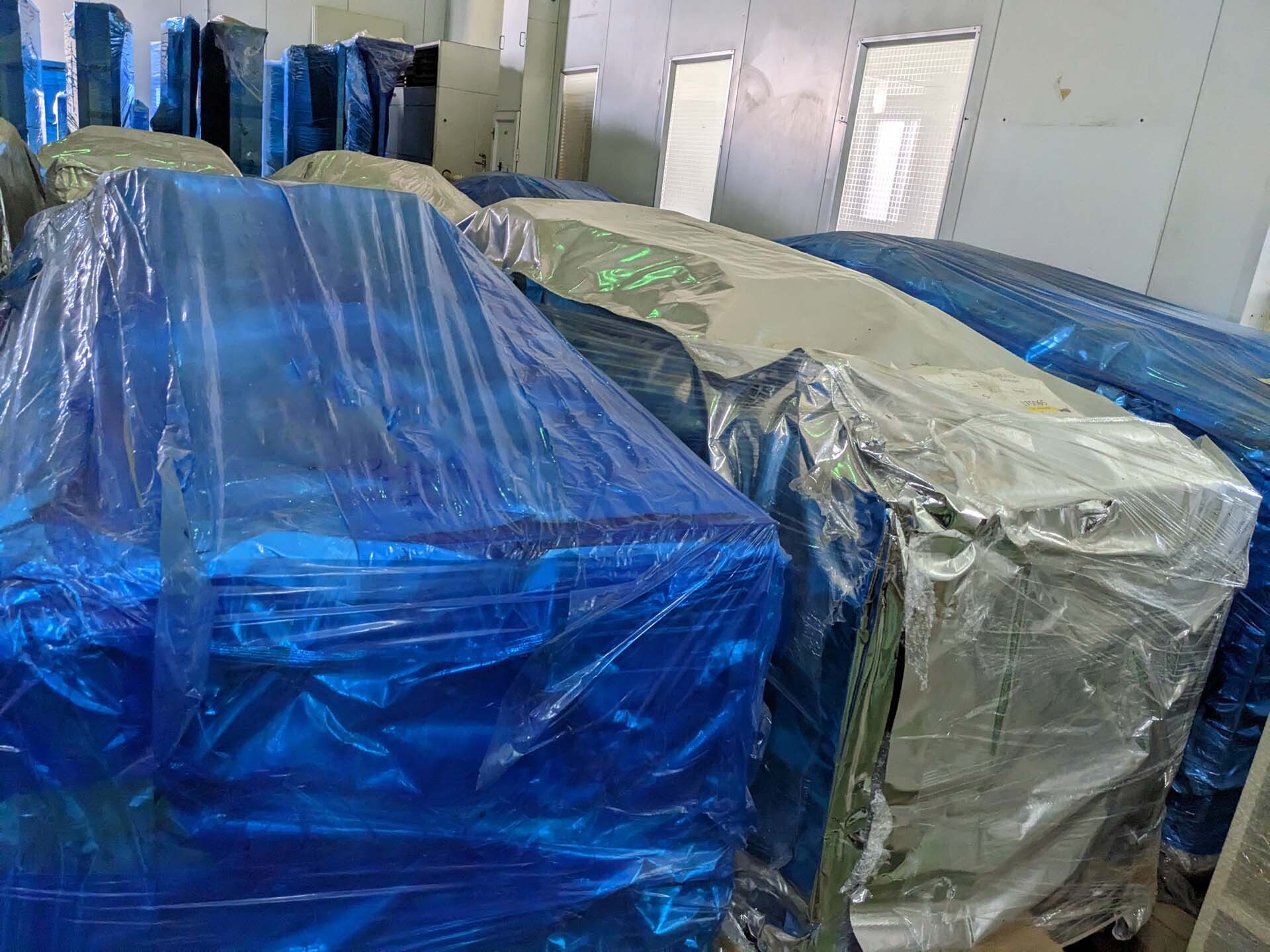
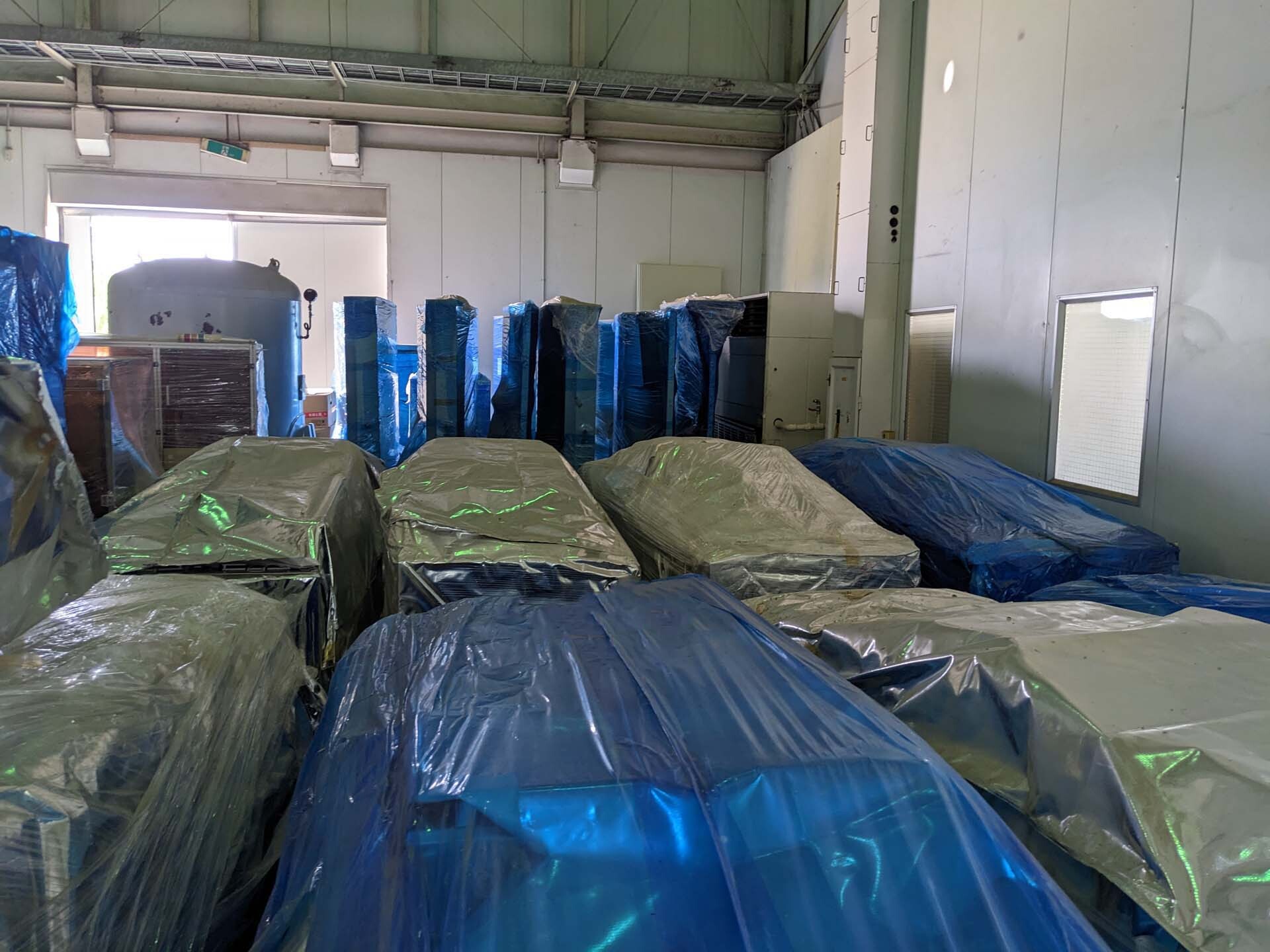
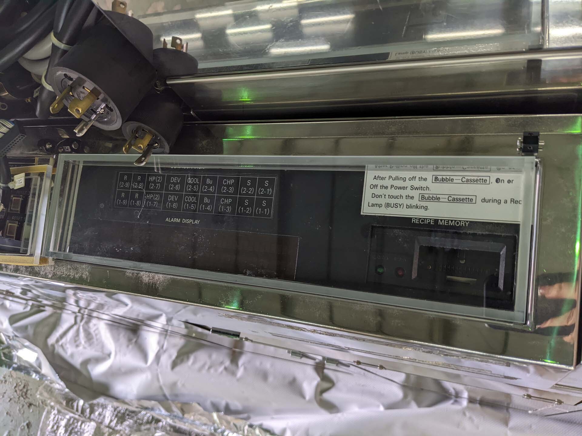
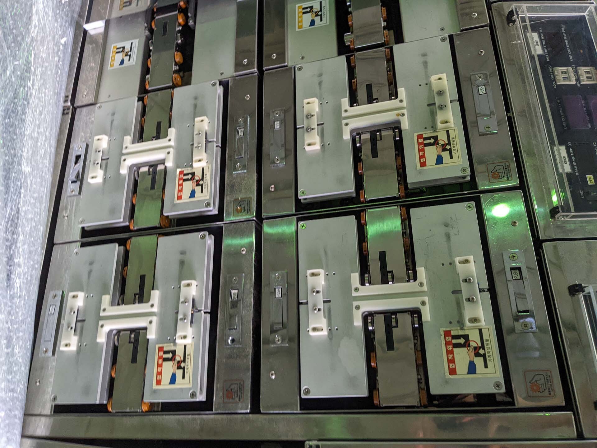
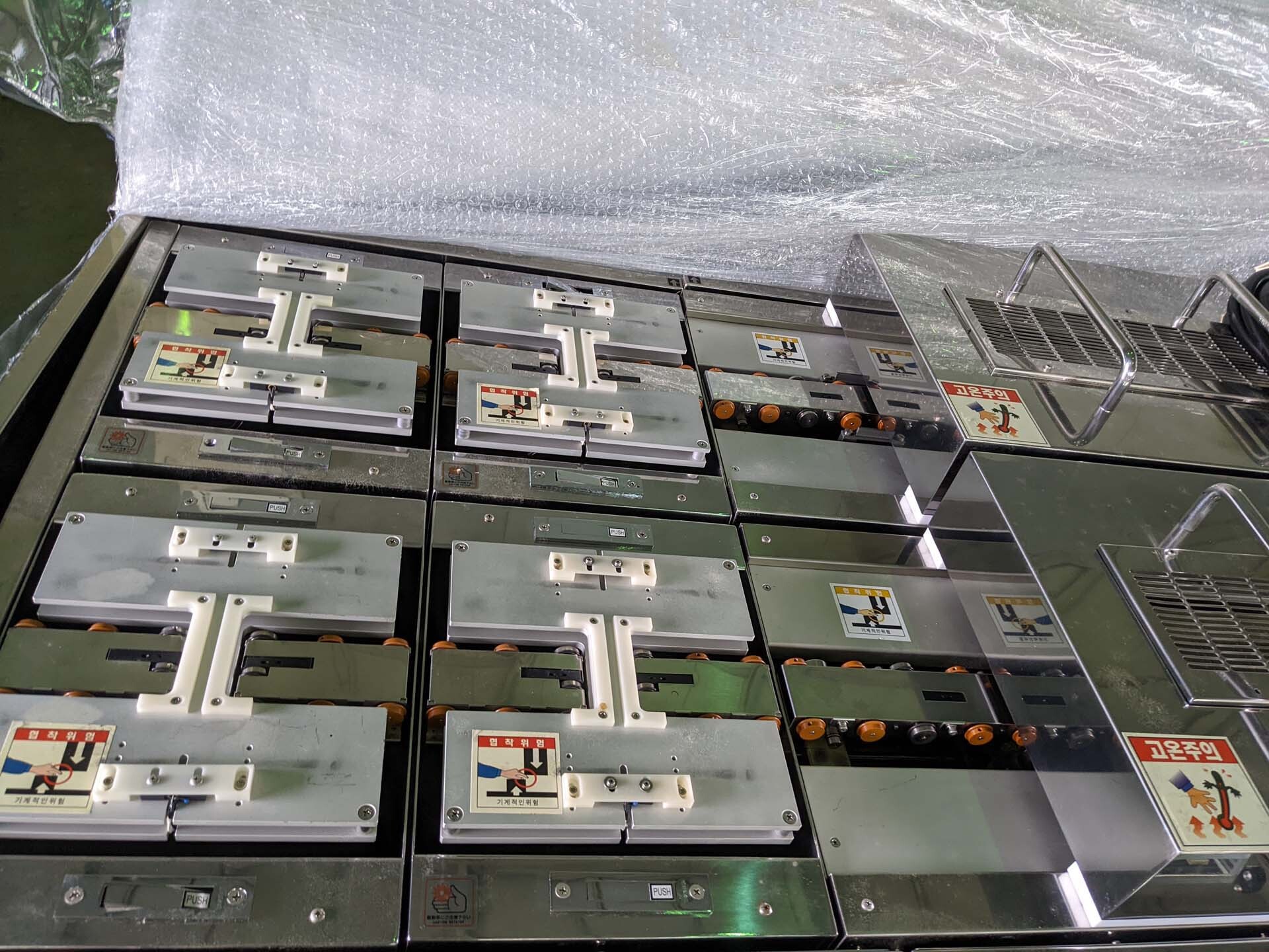
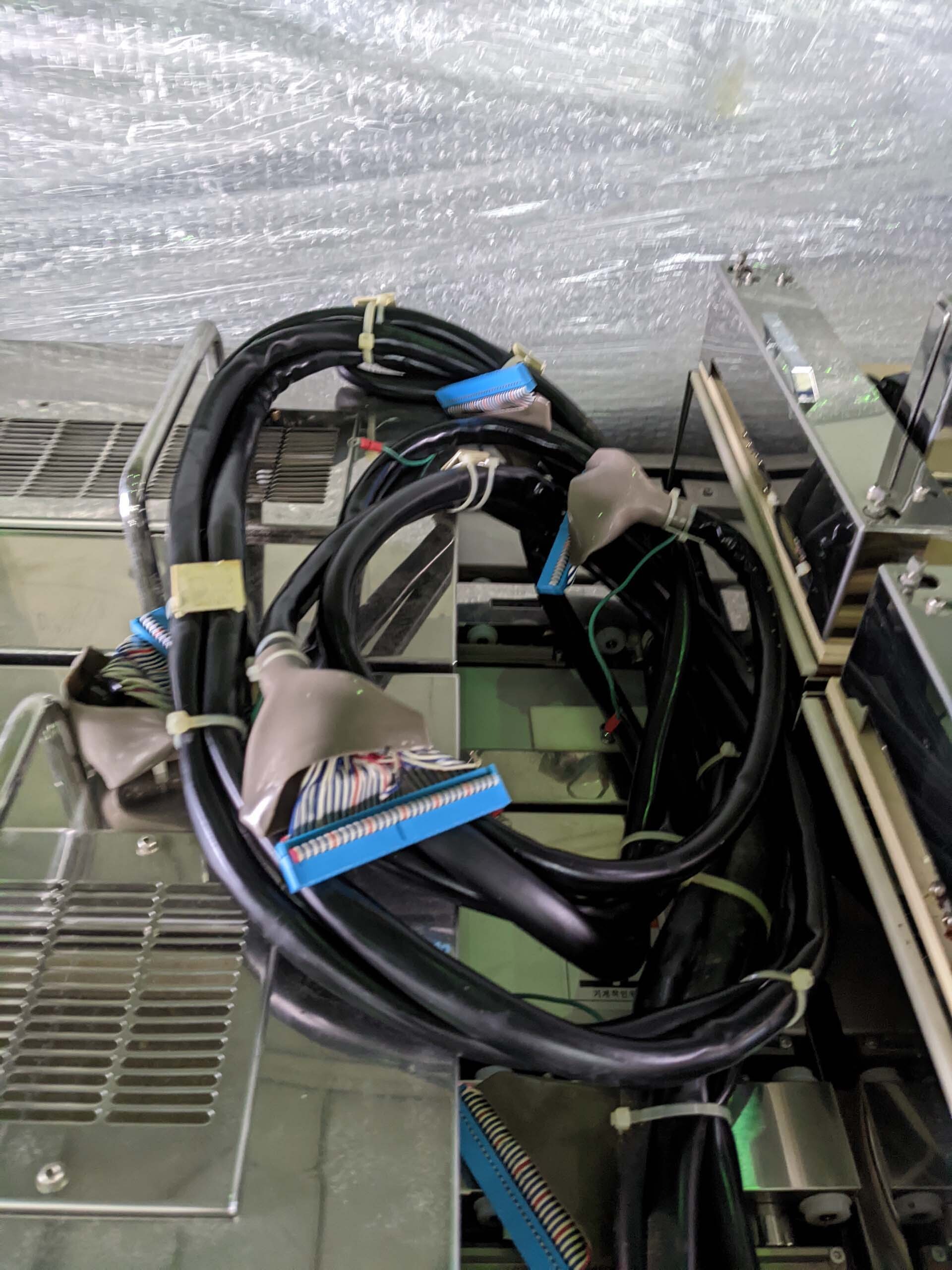
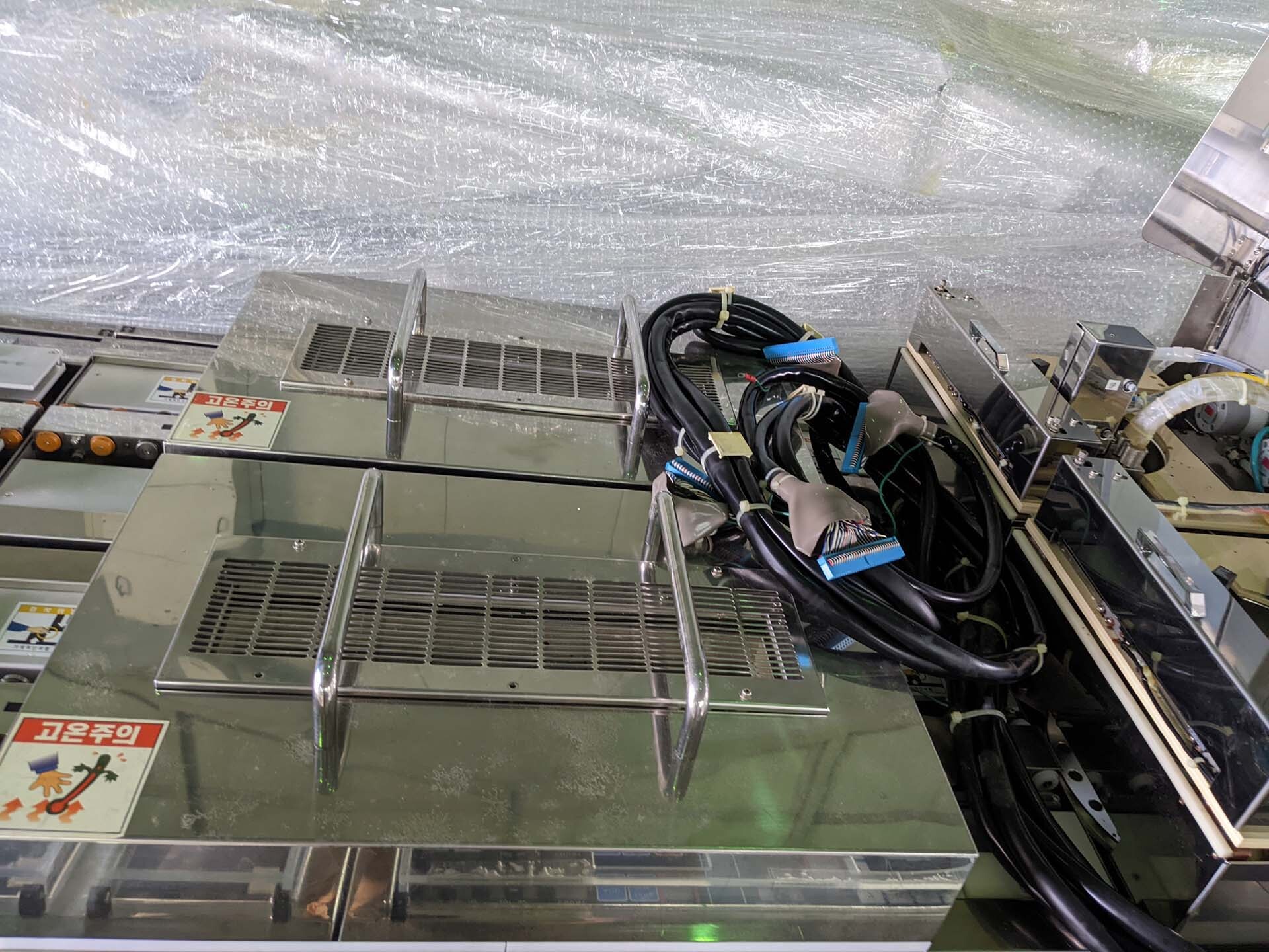
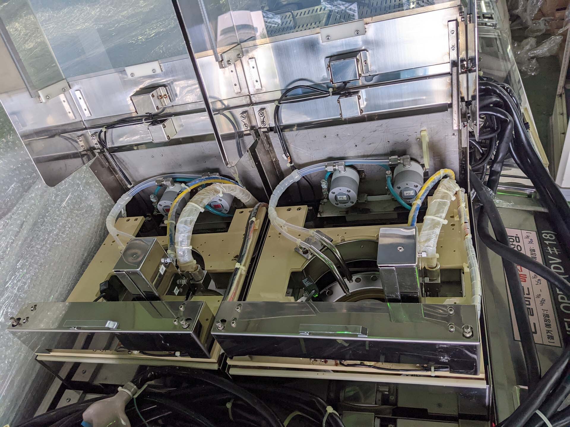
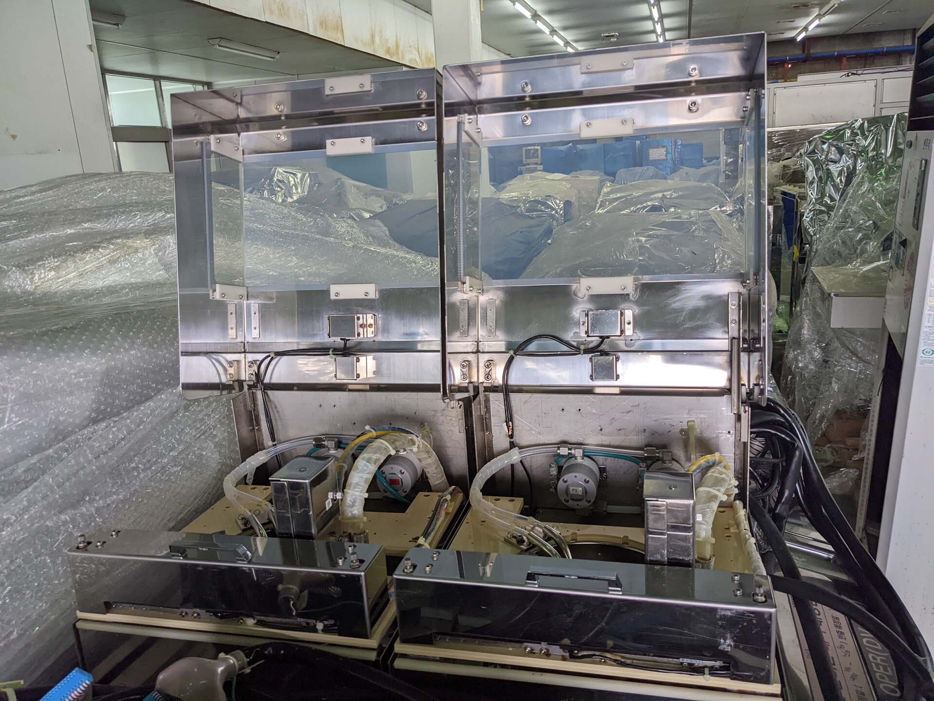
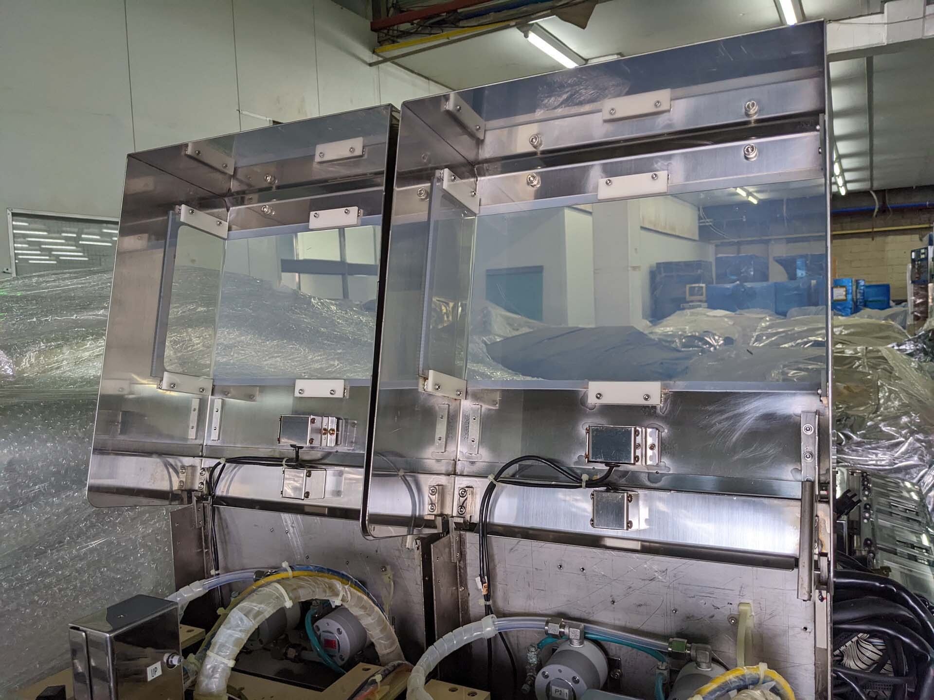
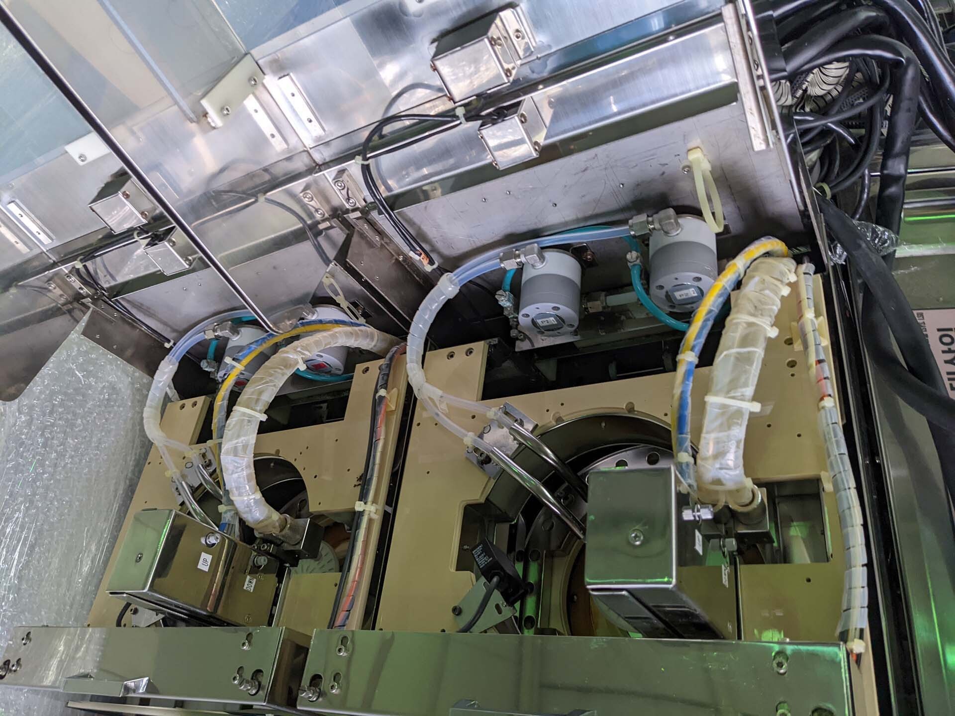
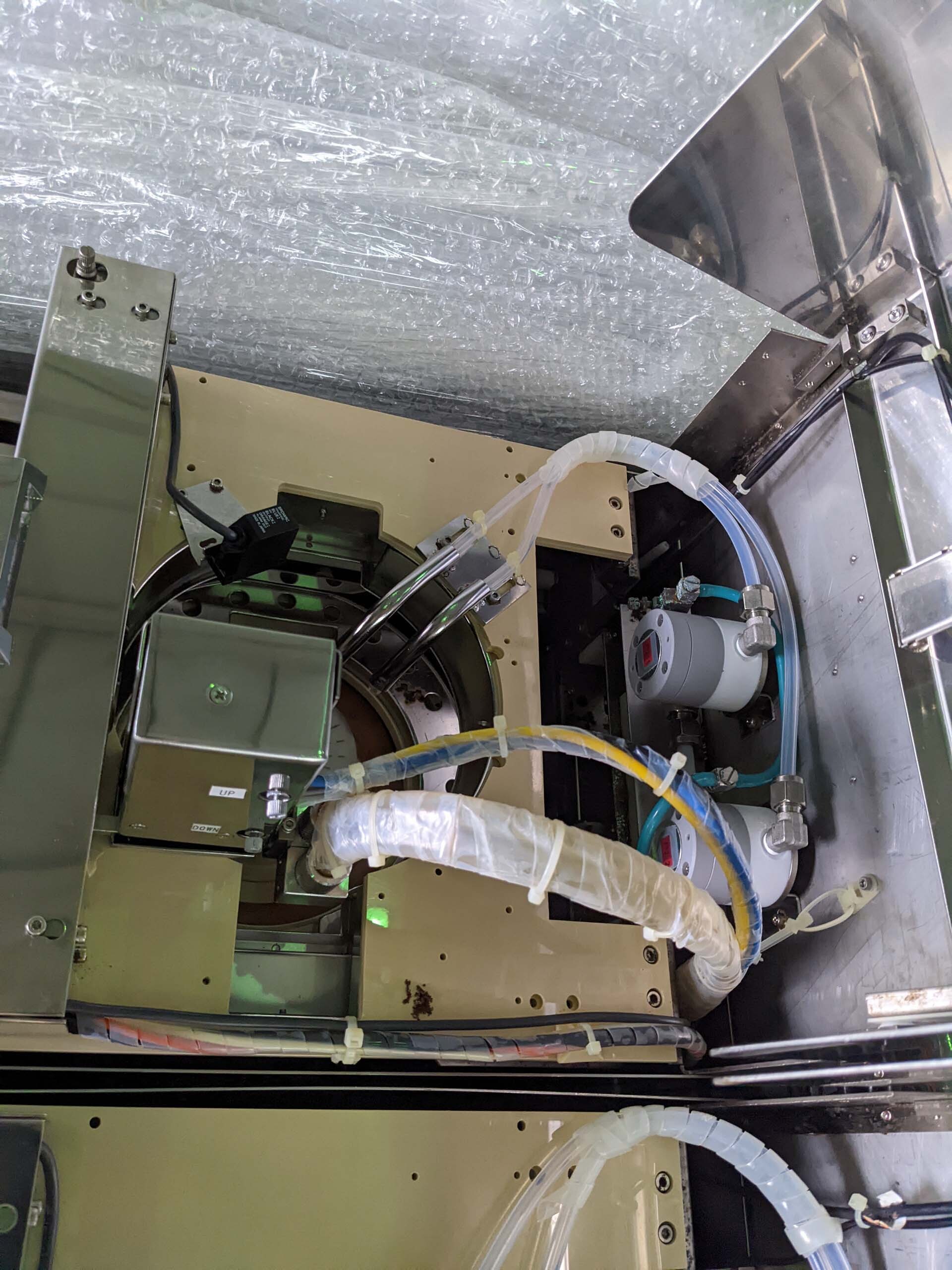
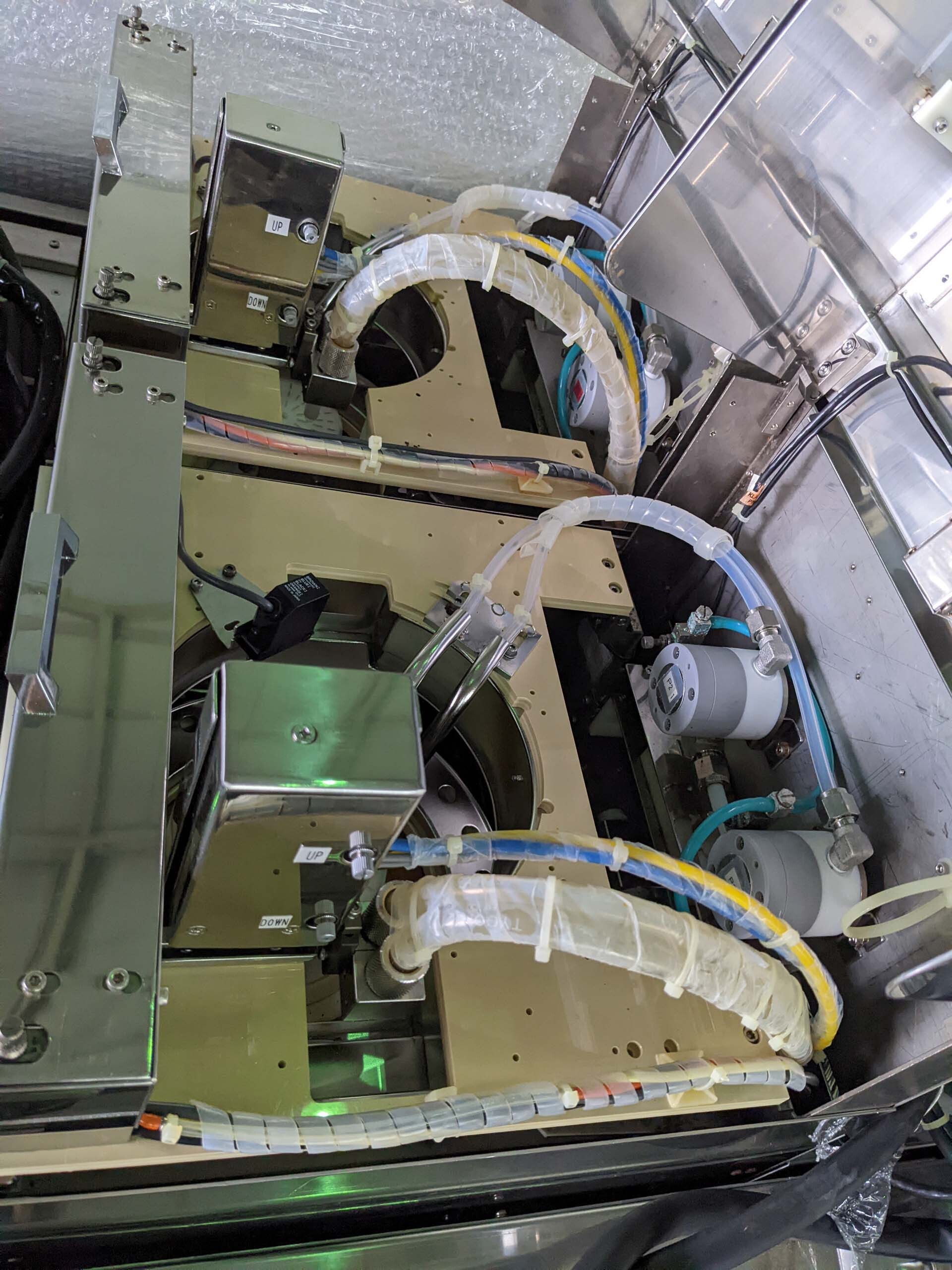
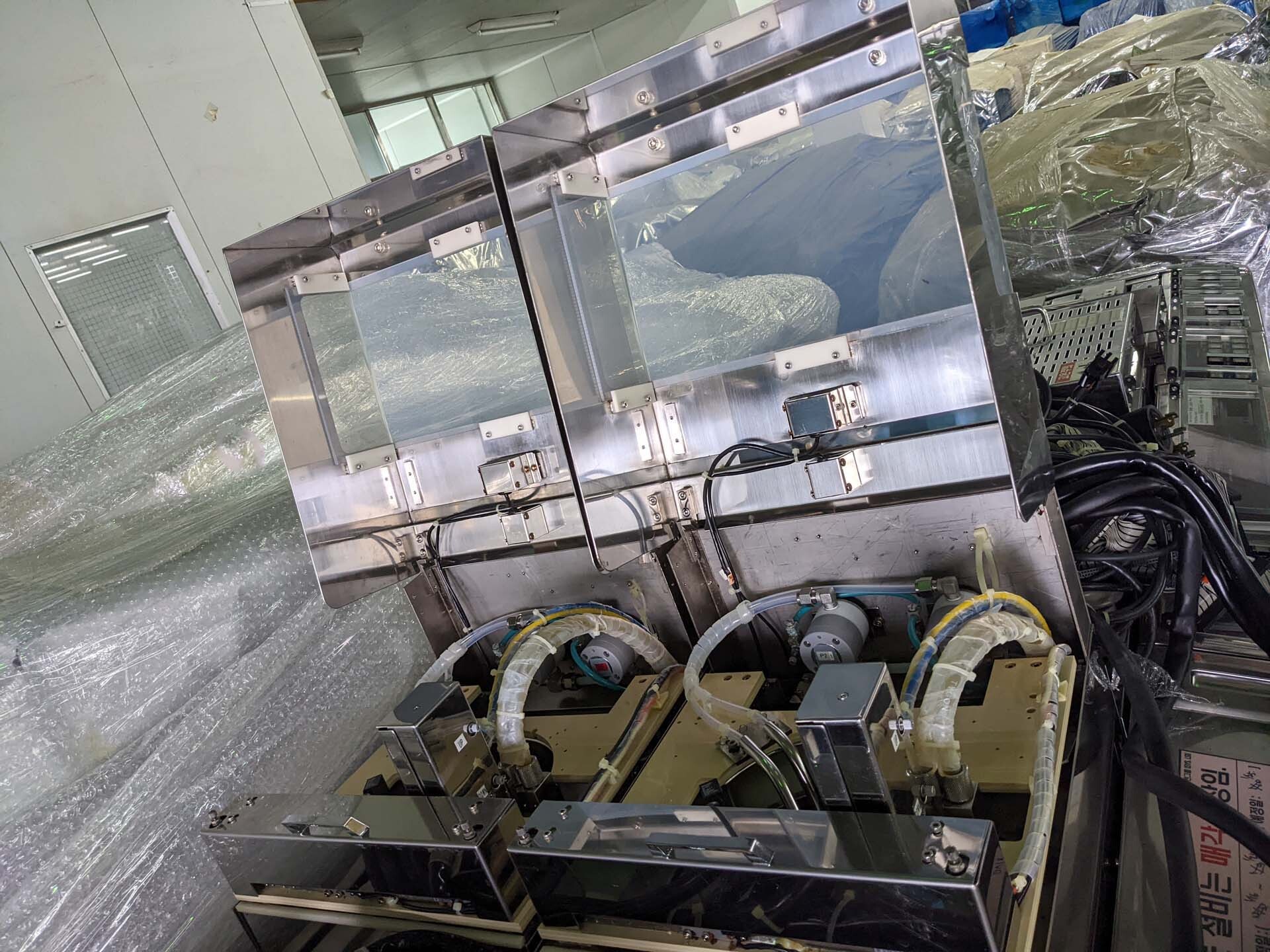
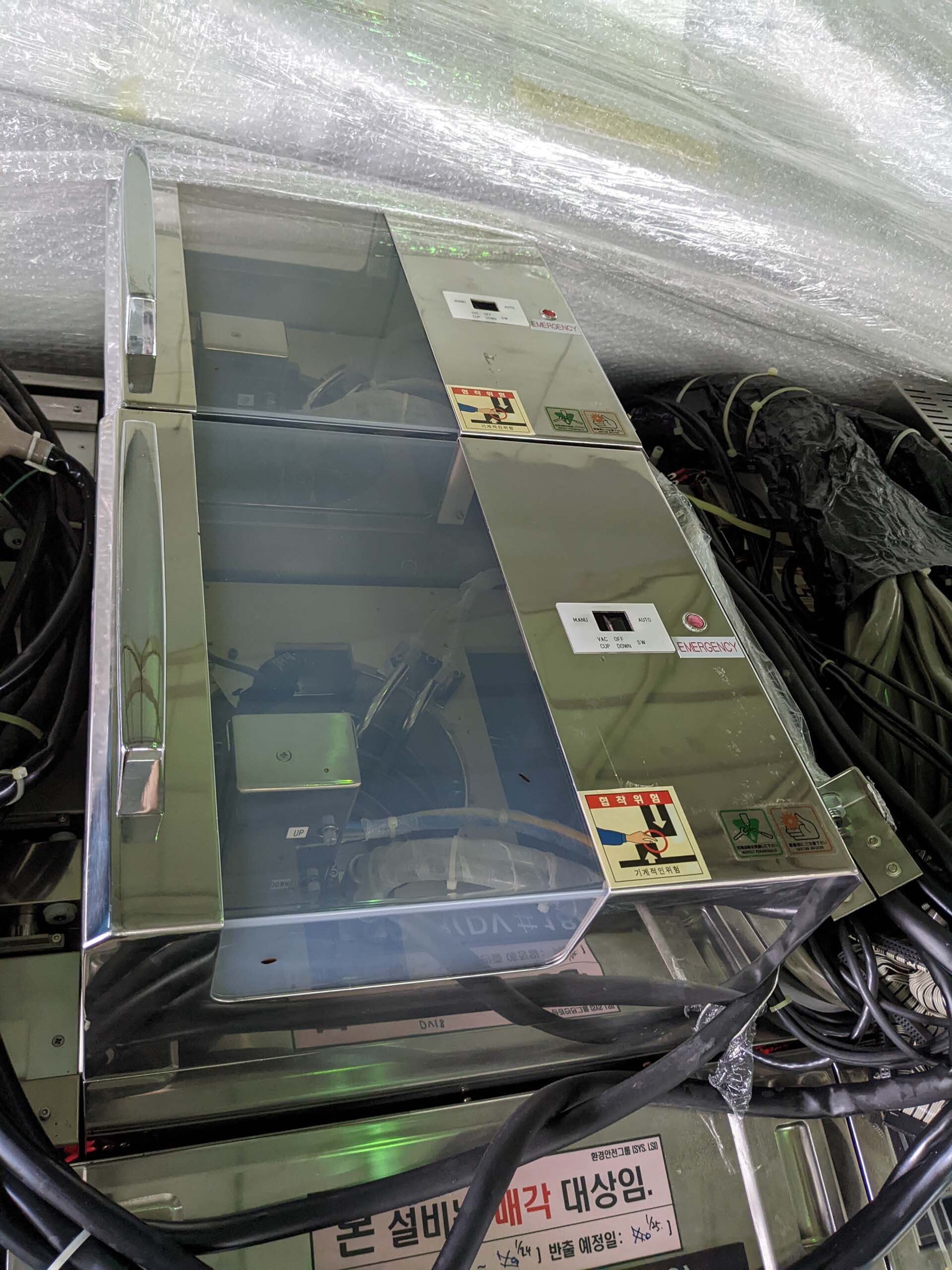
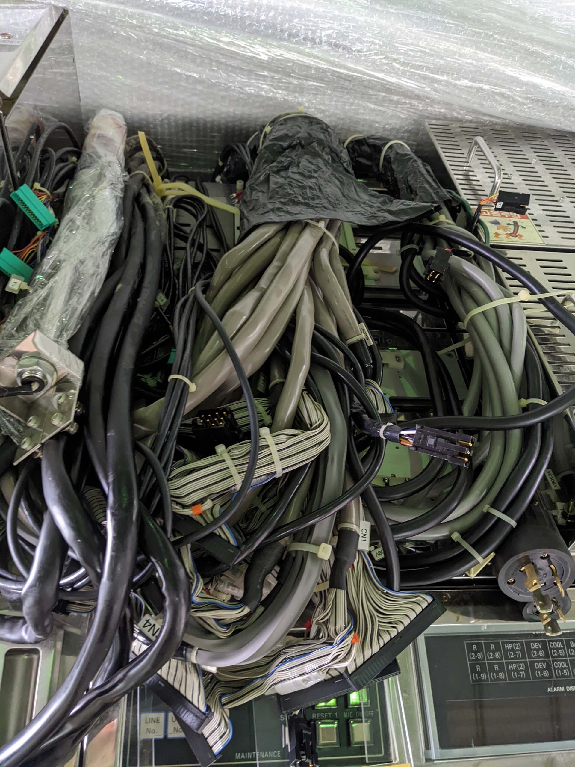
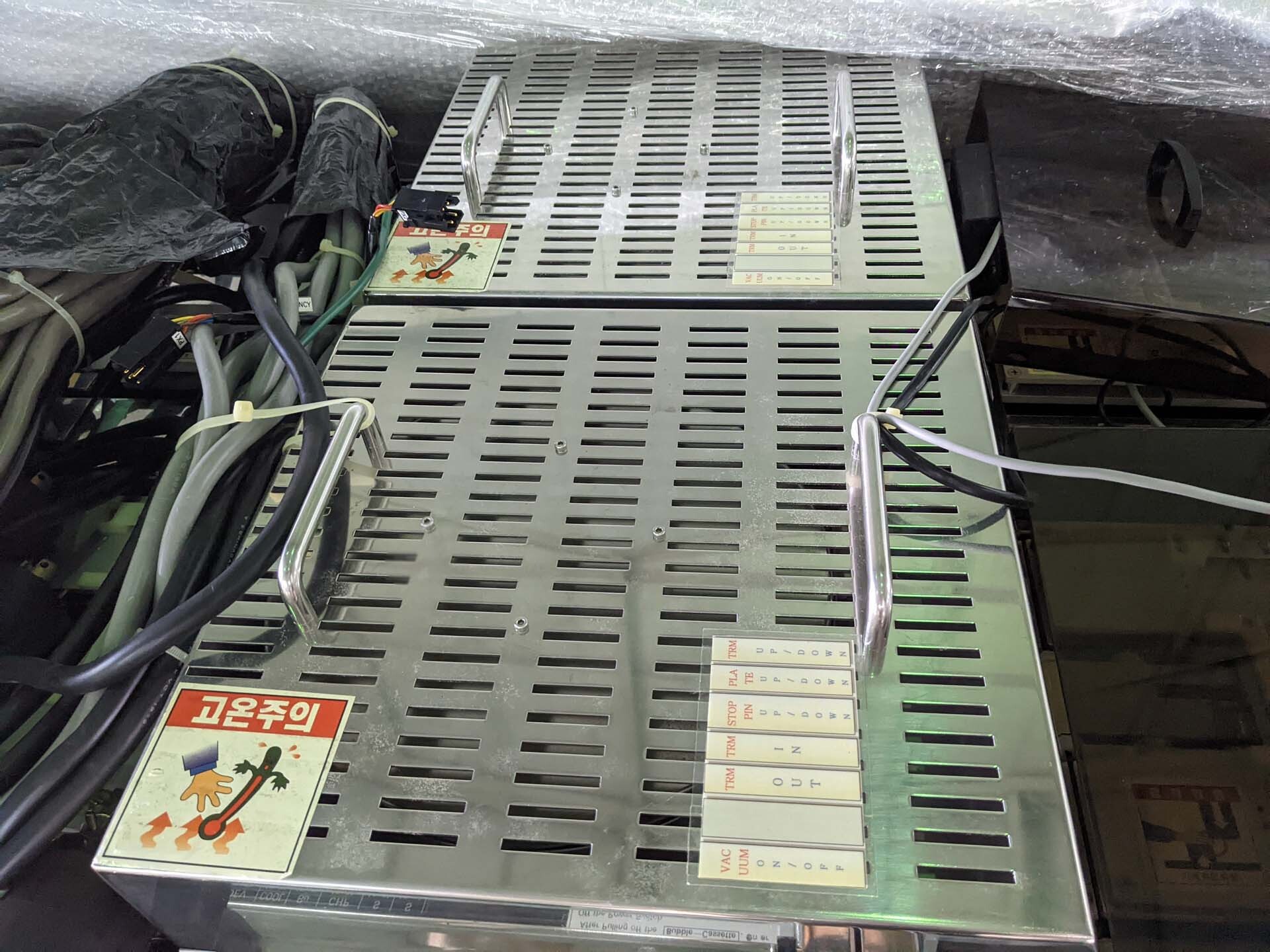
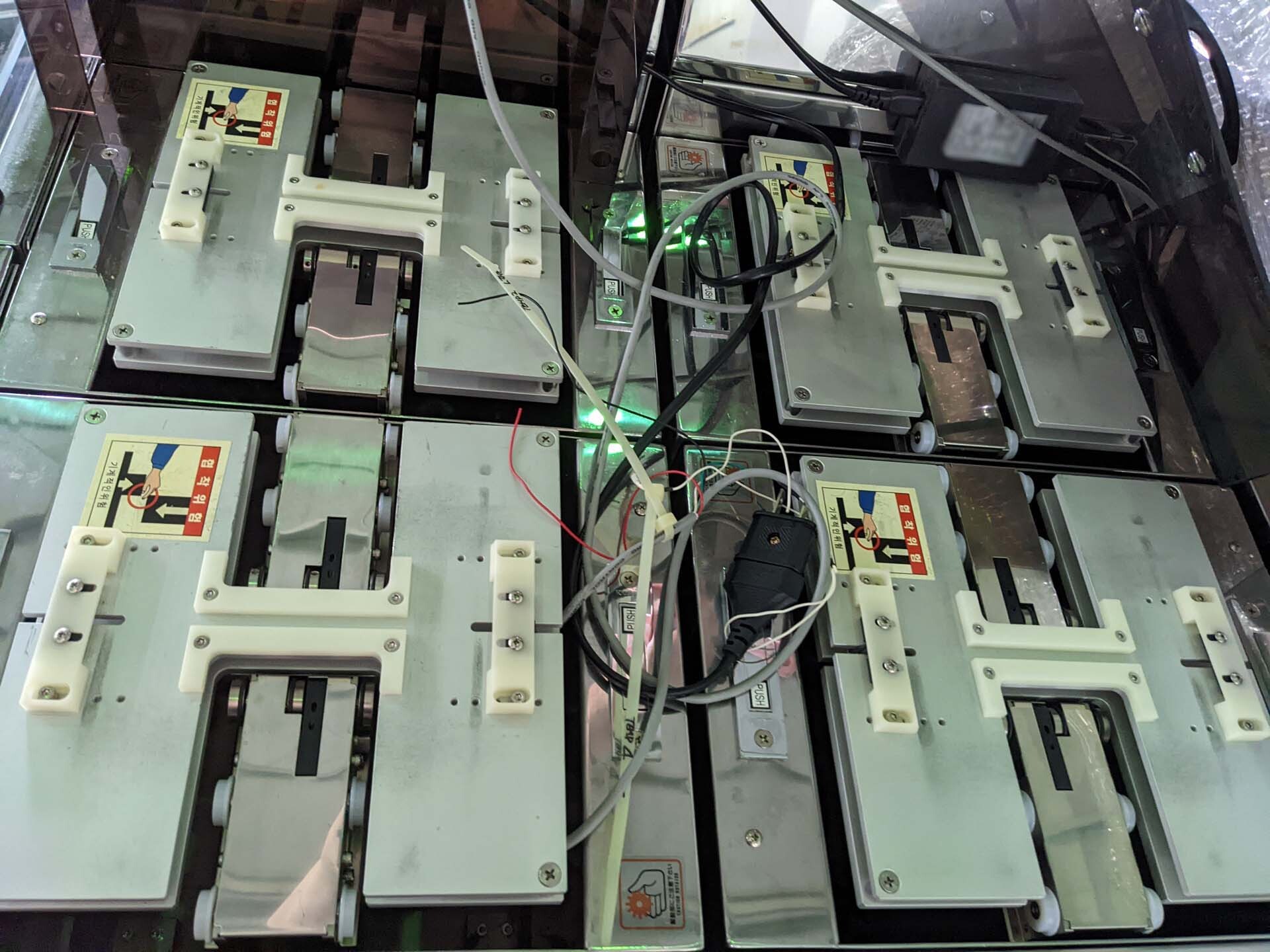
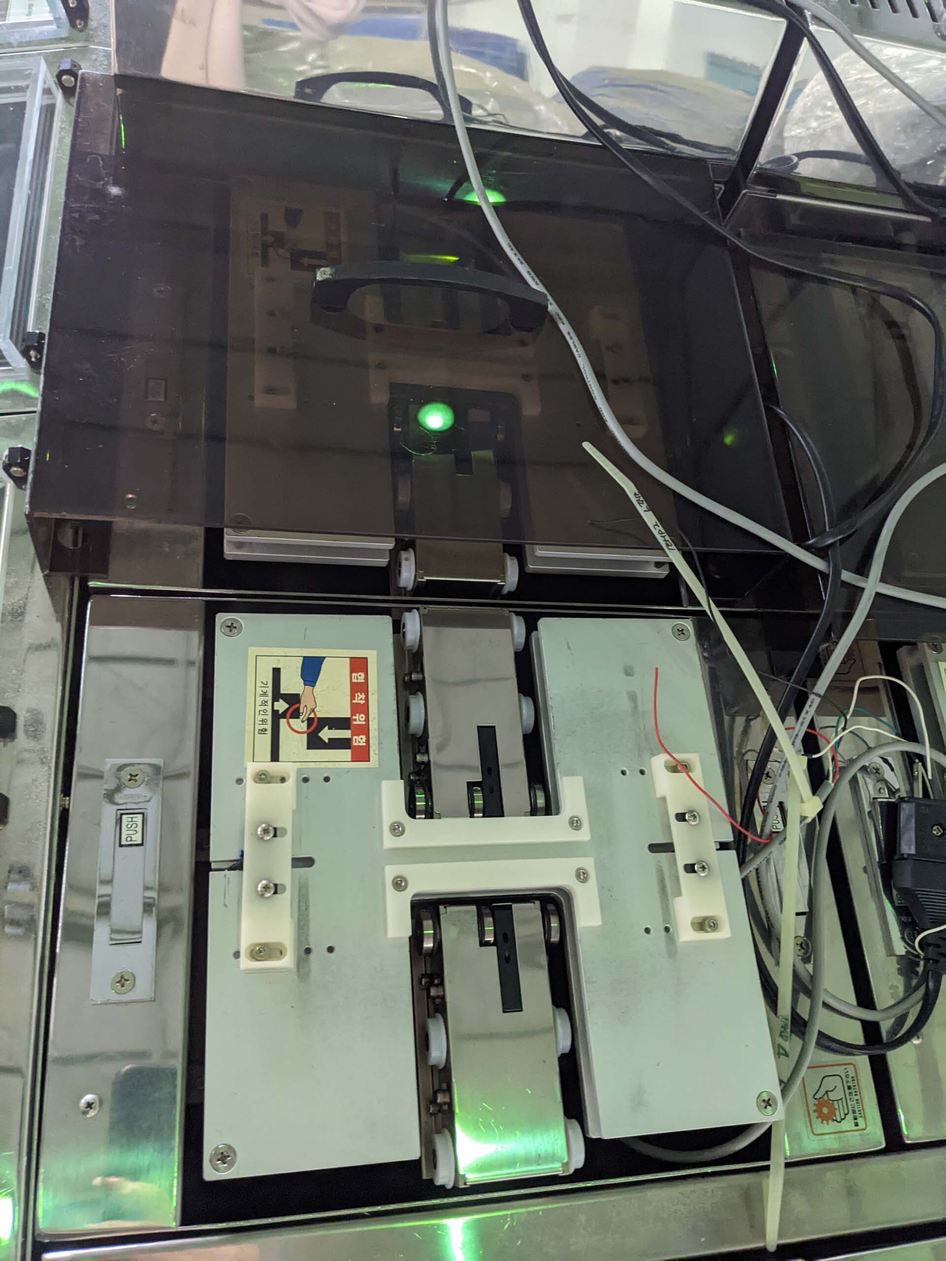
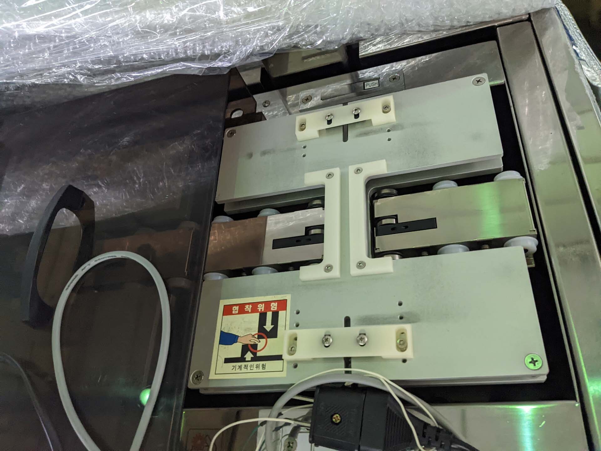
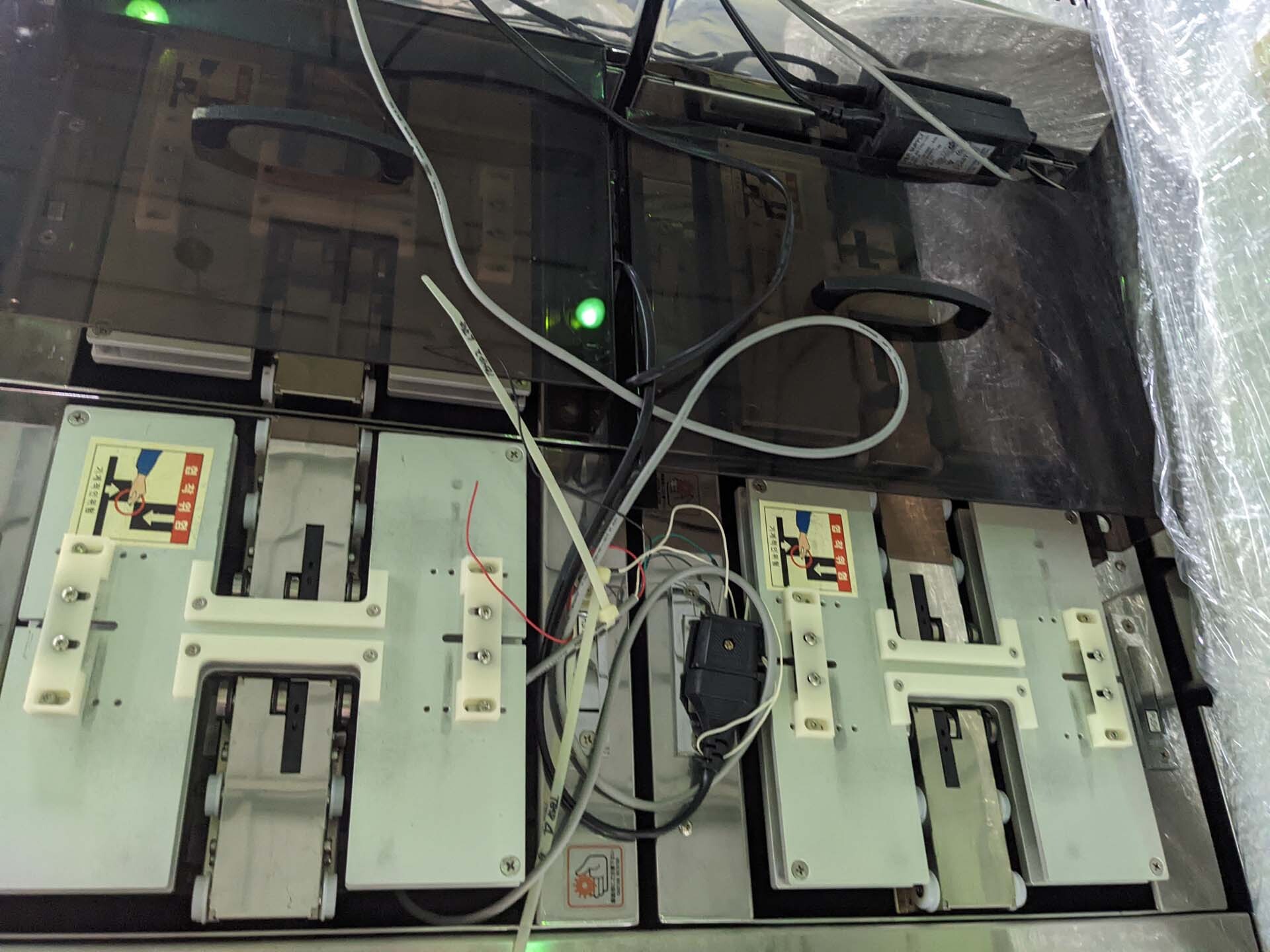
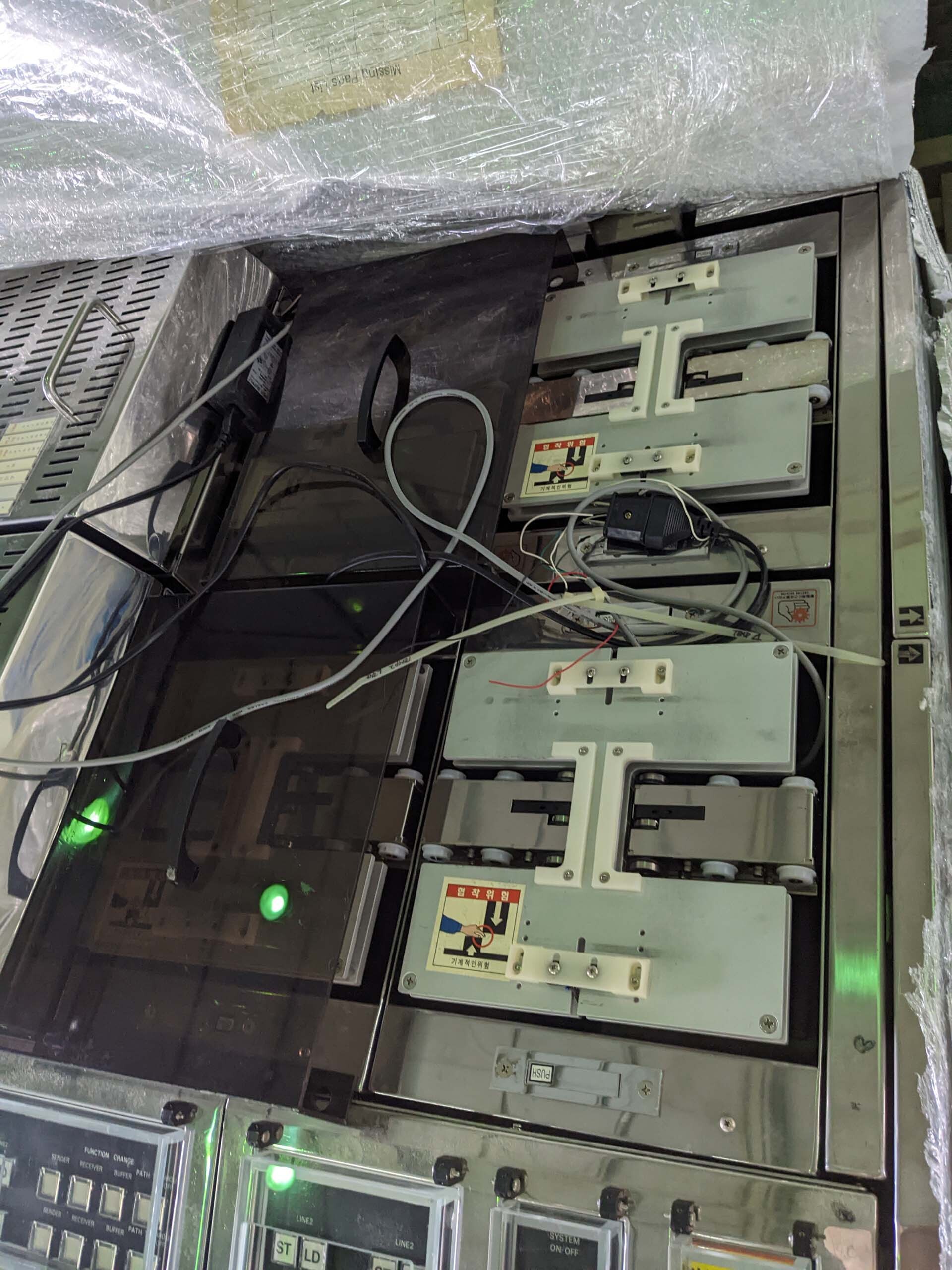
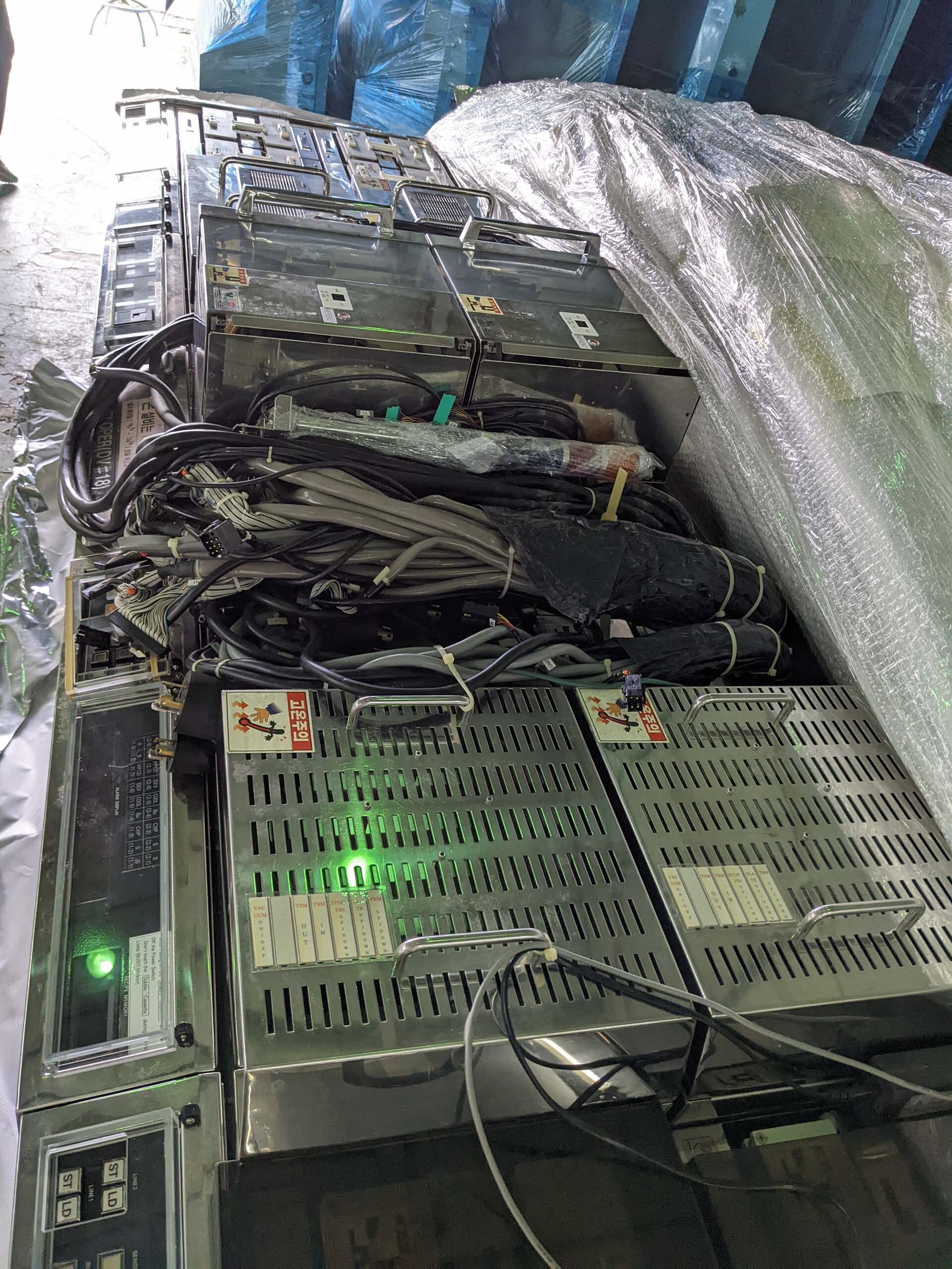
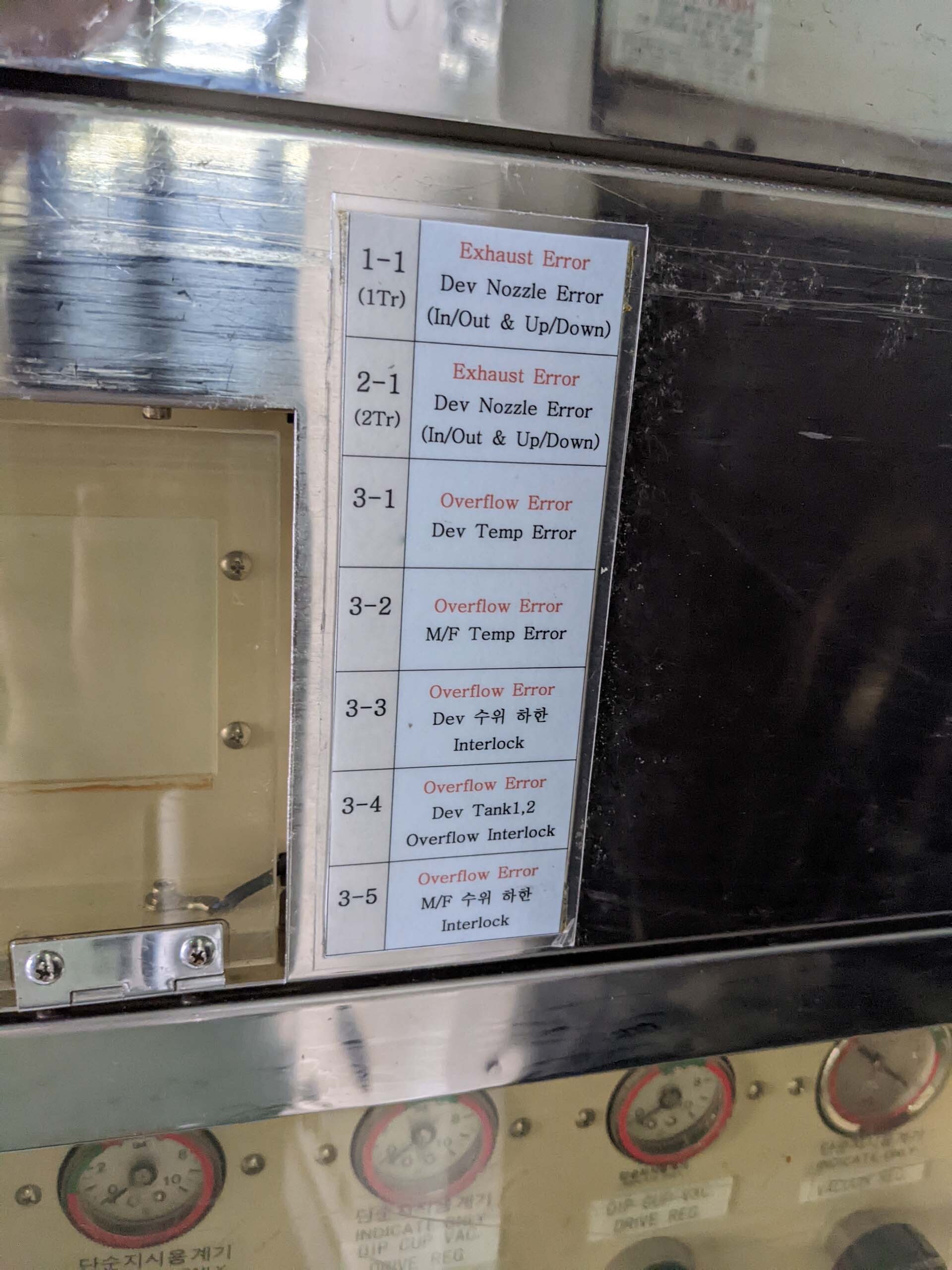
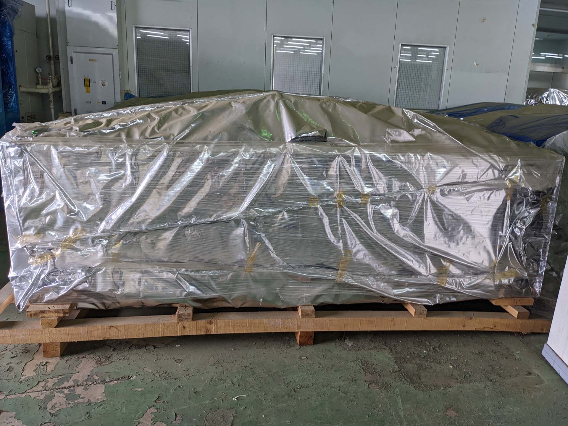
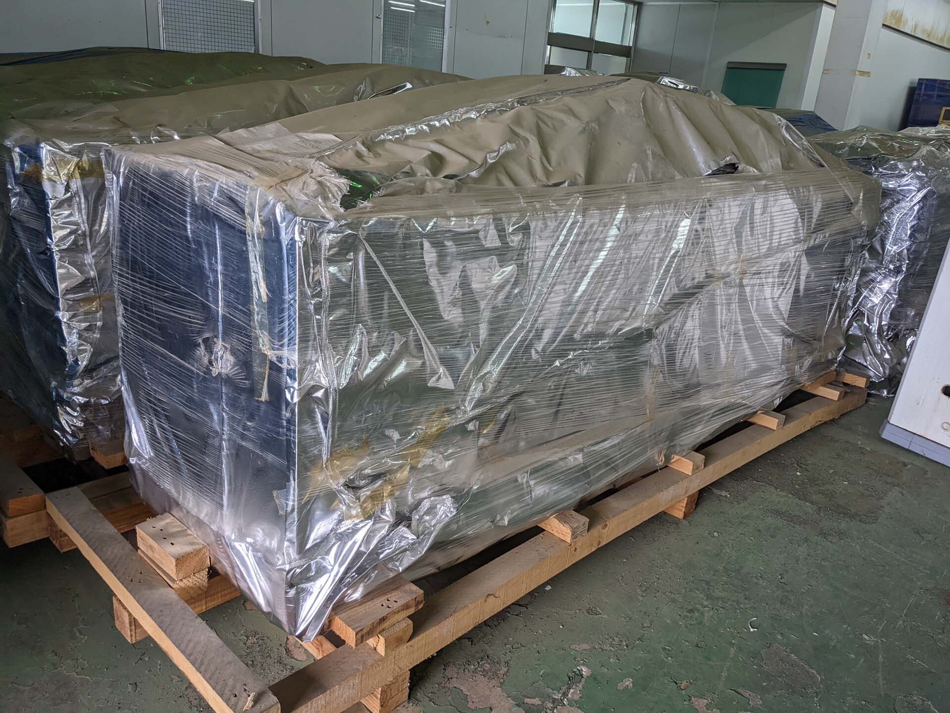
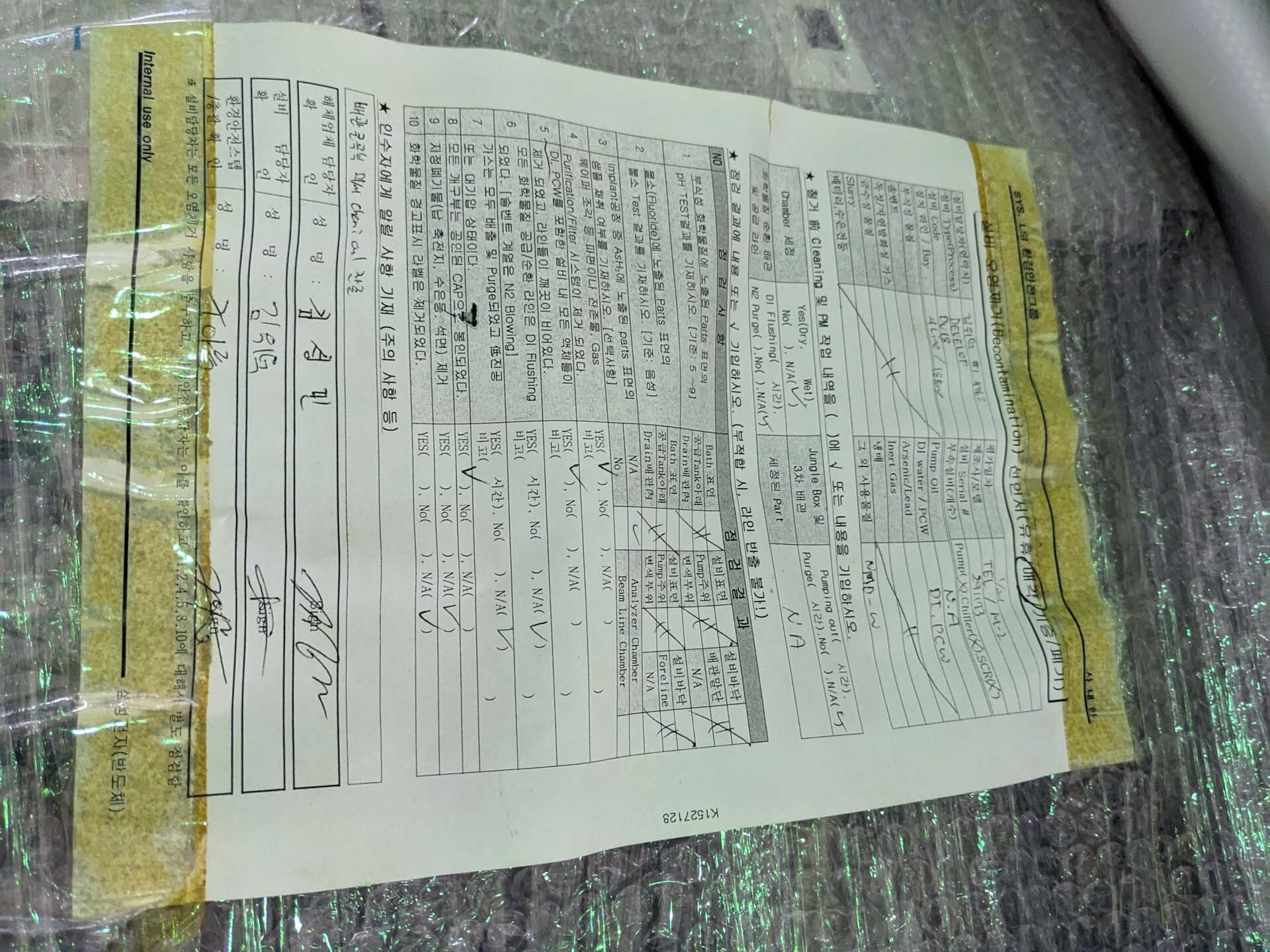
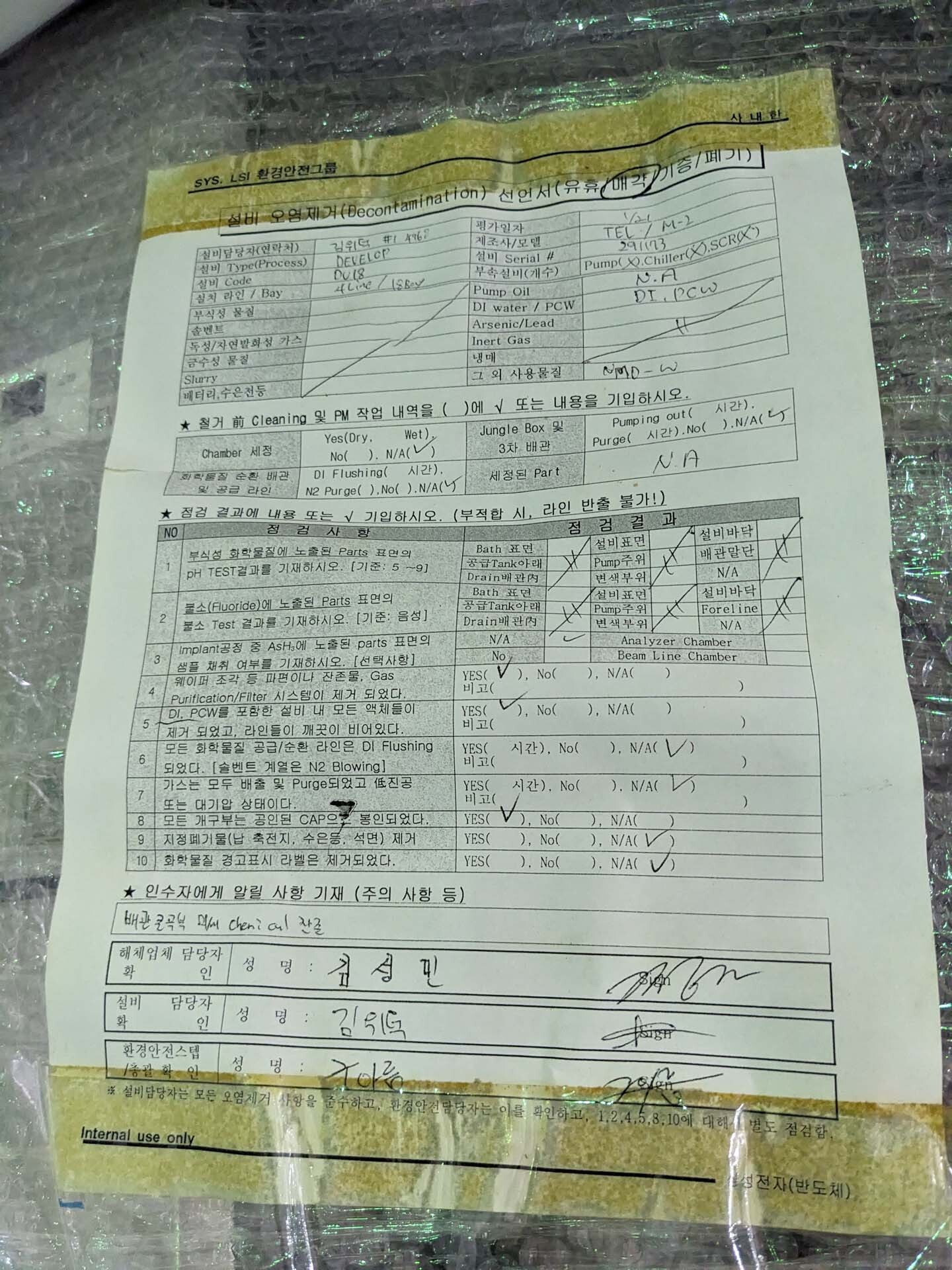
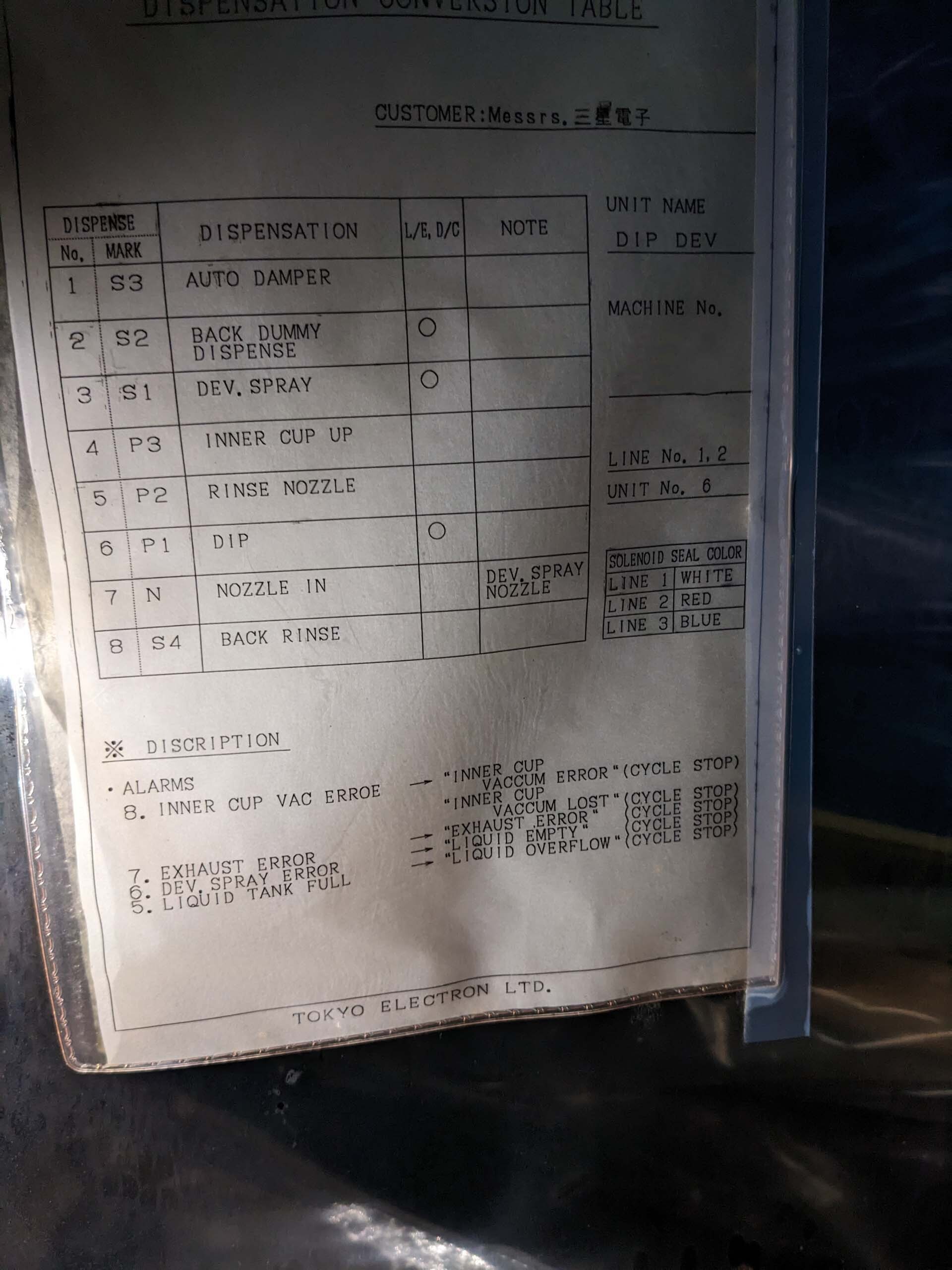
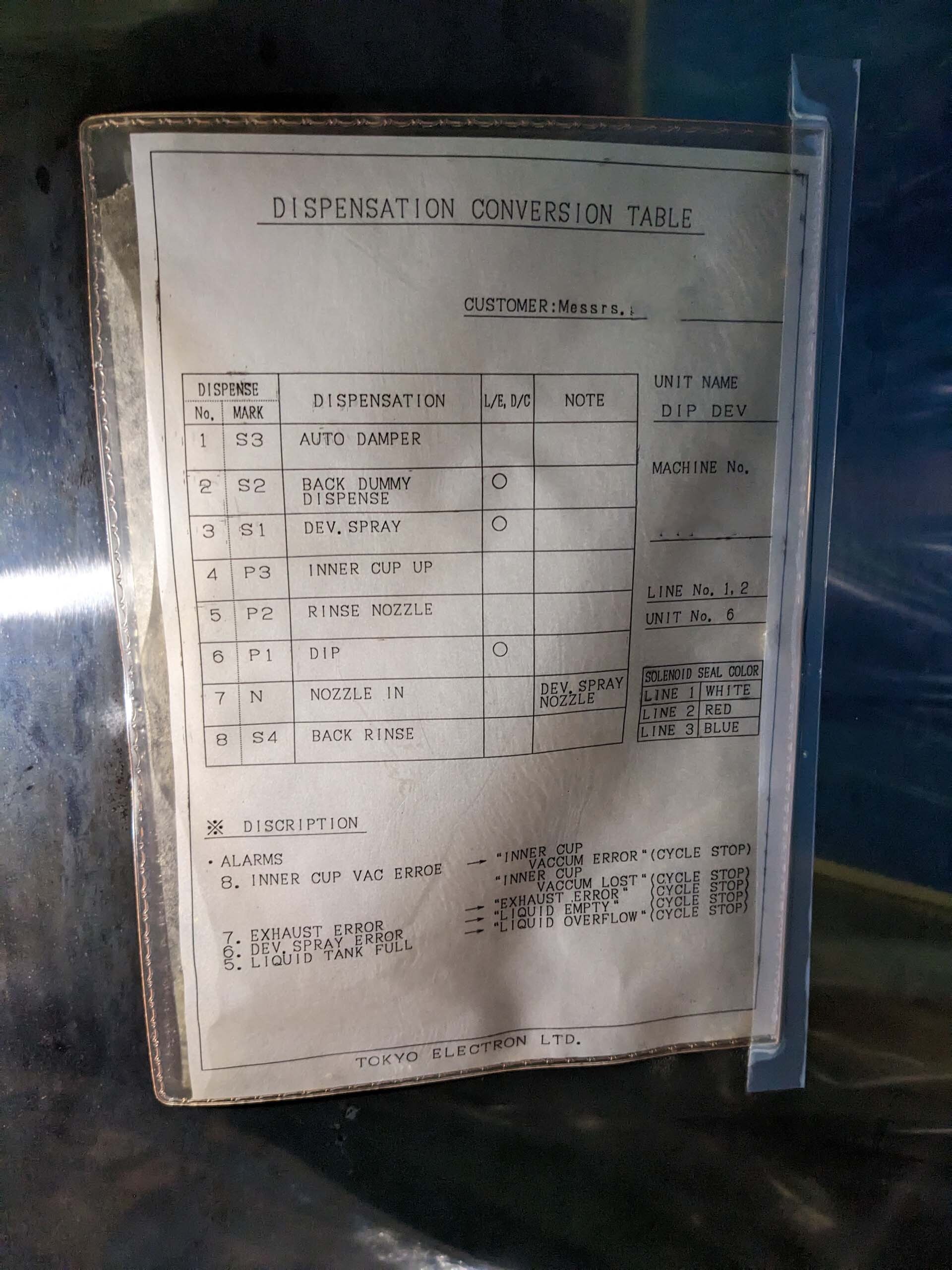
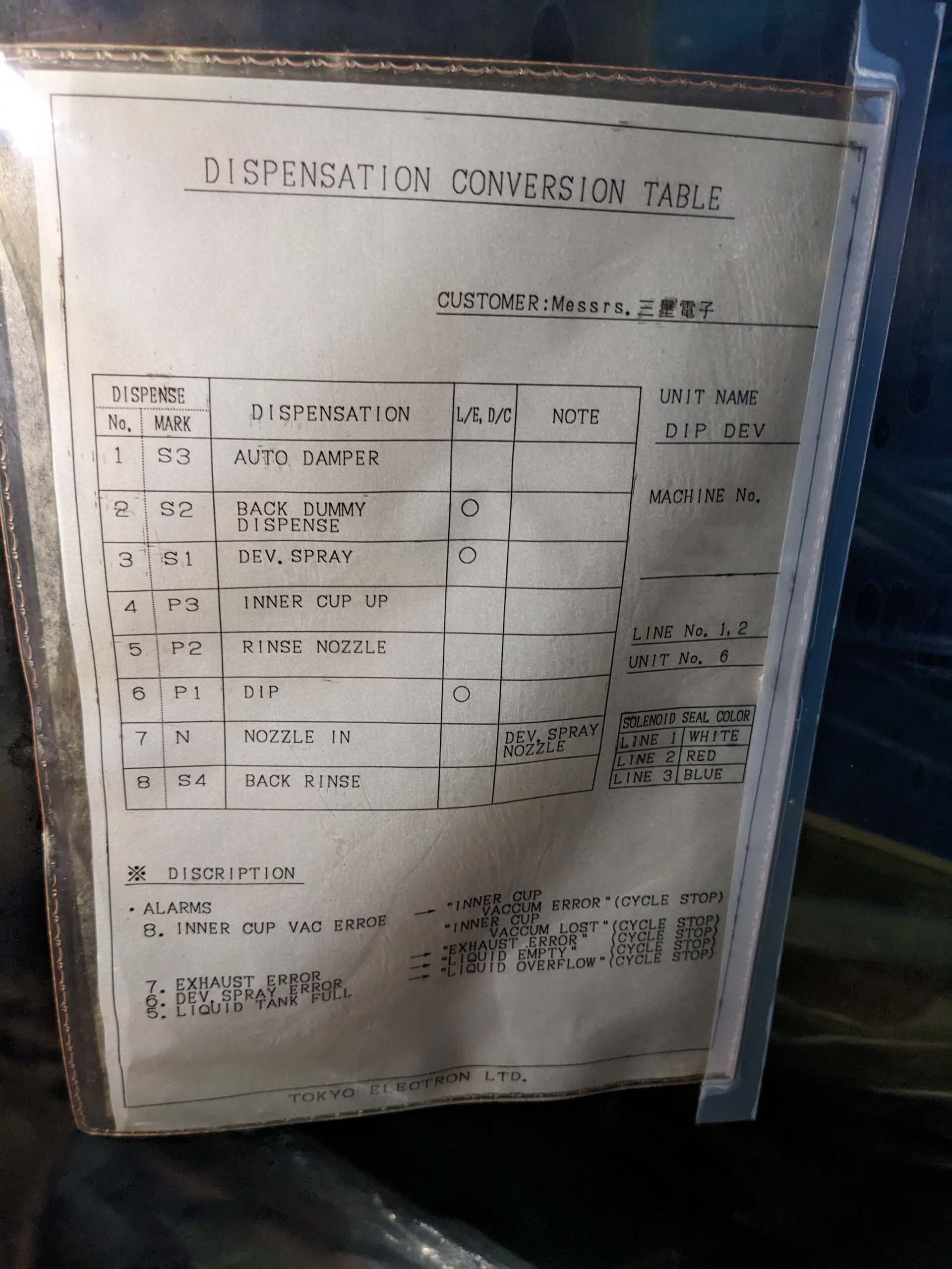
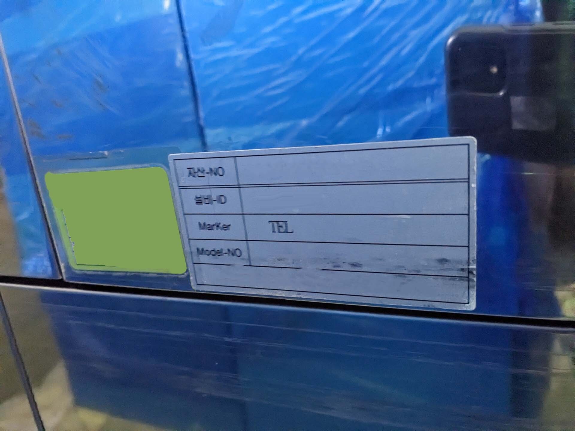
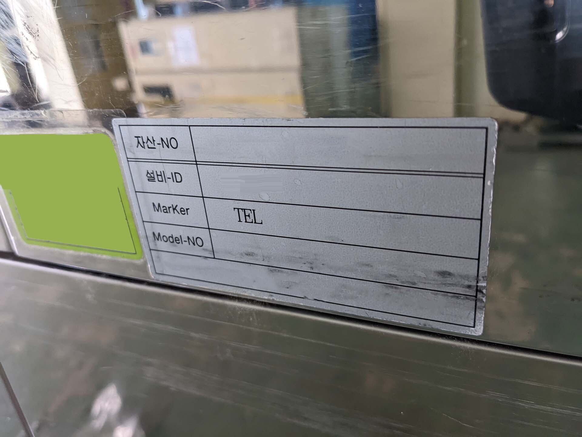
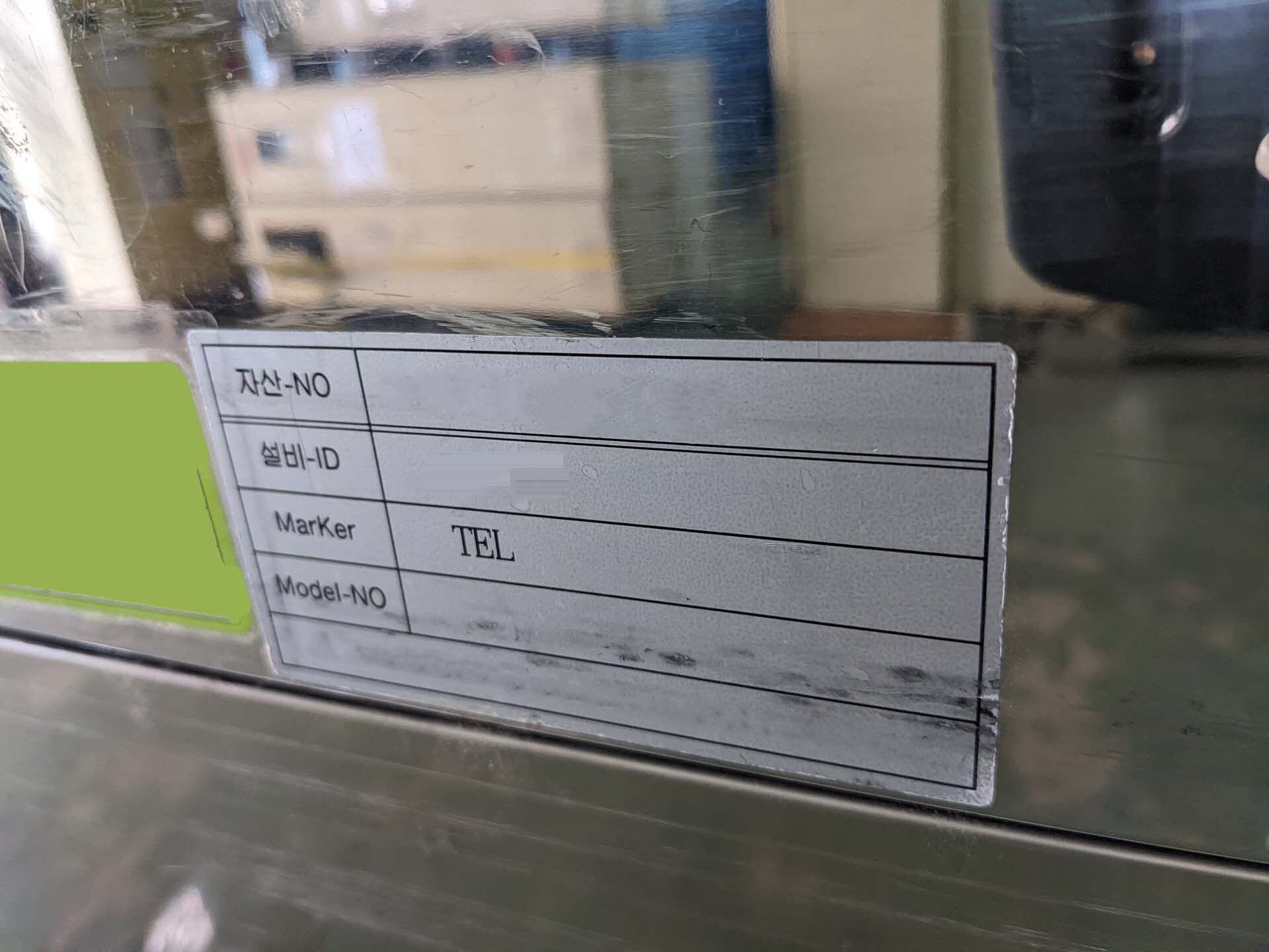
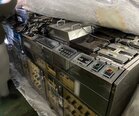
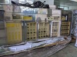
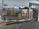
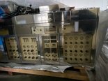
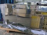
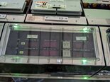
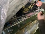
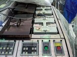
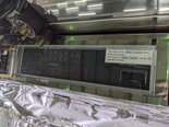
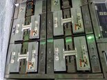
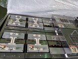
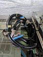
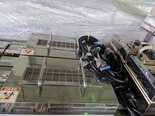
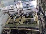
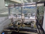
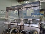
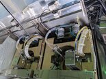
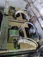
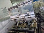
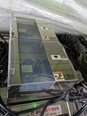
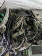
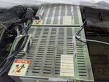
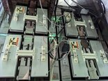
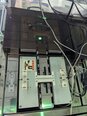
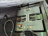
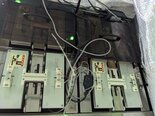
TEL / TOKYO ELECTRON MARK II is one of the most advanced photoresist systems on the market. It is used to create lithographic patterns on a substrate, typically a semiconductor. TEL MARK II equipment employs two main components to do this: a source of ultraviolet light and a projective lithography lens. The source of ultraviolet light is used to irradiate a light-sensitive photoresist material that coats the substrate. The projective lithography lens is then used to focus this light onto the substrate, creating a highly-accurate pattern on the surface. TOKYO ELECTRON MARK II system is designed for applications that require tight control of the light irradiation and accurate pattern definition. The photomask is scanned in a high-resolution manner to ensure an optimal definition of the patterns, and the light source used is designed for maximum consistency. In addition, the photoresist can be automatically dispensed across the substrate in different patterns, allowing for complete control over the pattern definition. MARK II unit is designed to be fully integrated, offering a compact, efficient and cost-effective solution for photoresist processes. The photomask can be changed without the need to open the unit, and the machine includes image output options for pattern comparison and archiving of results. The tool is controlled by a sophisticated automation asset, allowing for quick and easy set-up of recipes and operations. A range of accessories are also available with TEL / TOKYO ELECTRON MARK II model, including automated slitters, edge bevelers and spinners. These accessories help to ensure accuracy and repeatability of the photoresist process. TEL MARK II photoresist equipment is also fully compatible with advanced process control systems, such as EDAX signal processing software, allowing for further sophistication and control of the photoresist process. Overall, TOKYO ELECTRON MARK II photoresist system is a highly advanced, automated solution for advanced photolithography processes. The unit is designed for accuracy and repeatability, and with its features, accessories, and compatibility with advanced process control systems, offers the flexibility needed for complex and demanding lithography applications.
There are no reviews yet