Used TEL / TOKYO ELECTRON MARK II #293698881 for sale
URL successfully copied!
Tap to zoom
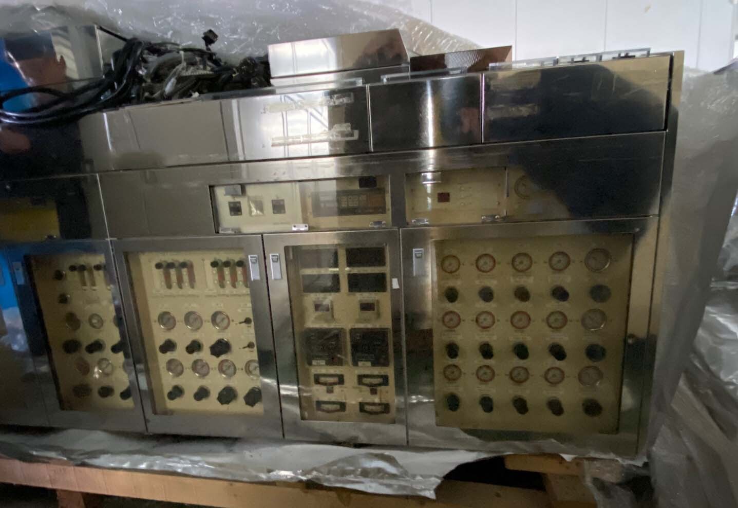

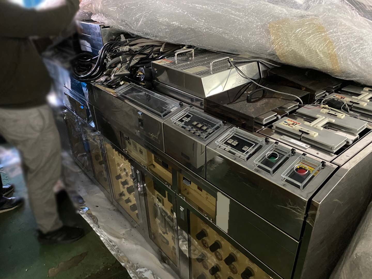
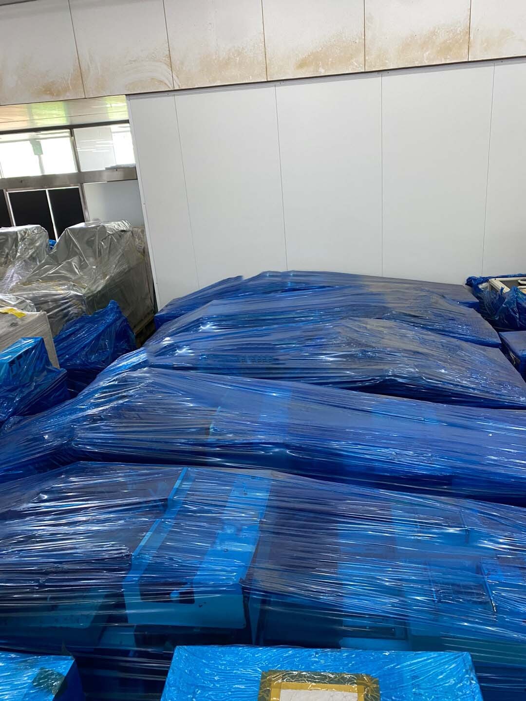
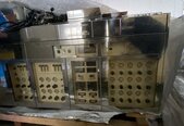
TEL / TOKYO ELECTRON MARK II is a state-of-the-art photoresist equipment that plays a crucial role in the advanced semiconductor manufacturing process. Developed by TEL Ltd., a leading company in the field of semiconductor production equipment, TEL MARK II represents a significant advancement in photoresist technology, offering unparalleled precision, reliability, and efficiency. Photoresist systems are essential in the fabrication of integrated circuits (ICs) and other semiconductor devices. They are used to transfer intricate patterns onto silicon wafers, which serve as the foundation for electronic components in devices such as smartphones, computers, and automotive systems. TOKYO ELECTRON MARK II system is designed to achieve sub-micron resolution and tight control over critical dimensions, enabling the production of cutting-edge semiconductor devices with high performance and reliability. One of the key features of MARK II is its advanced exposure technology. The unit utilizes advanced lithography techniques to create precise patterns on the wafer surface with extreme accuracy. This is achieved through a combination of high-resolution optics, sophisticated alignment systems, and precise control of exposure parameters such as dose, focus, and proximity effect correction. The result is the production of intricate patterns with sub-micron resolution, enabling the fabrication of next-generation semiconductor devices with complex geometries and high circuit densities. Another notable aspect of TEL / TOKYO ELECTRON MARK II machine is its advanced automation capabilities. The tool is equipped with sophisticated control software that allows for seamless integration into semiconductor manufacturing lines. This automation enables high-throughput production of ICs with minimal human intervention, reducing the risk of errors and improving overall process efficiency. TEL MARK II asset also features advanced wafer handling mechanisms, including robotic arms and wafer mapping technology, to ensure precise alignment and positioning during the exposure process. In addition to its technical capabilities, TOKYO ELECTRON MARK II excels in terms of reliability and uptime. The model is designed with rugged construction and high-quality components to ensure long-term stability and robust performance in demanding manufacturing environments. Furthermore, TOKYO ELECTRON provides comprehensive service and support for MARK II equipment, including maintenance, calibration, and technical assistance to maximize system uptime and productivity. Overall, TEL / TOKYO ELECTRON MARK II represents a significant advancement in photoresist technology, offering semiconductor manufacturers a state-of-the-art solution for producing advanced semiconductor devices with sub-micron resolution, high circuit densities, and superior performance. With its advanced exposure technology, automation capabilities, and reliability, TEL MARK II unit is poised to play a key role in the continued advancement of semiconductor technology and the production of cutting-edge electronic devices for various applications.
There are no reviews yet