Used TEL / TOKYO ELECTRON MARK II #293700414 for sale
URL successfully copied!







Tap to zoom
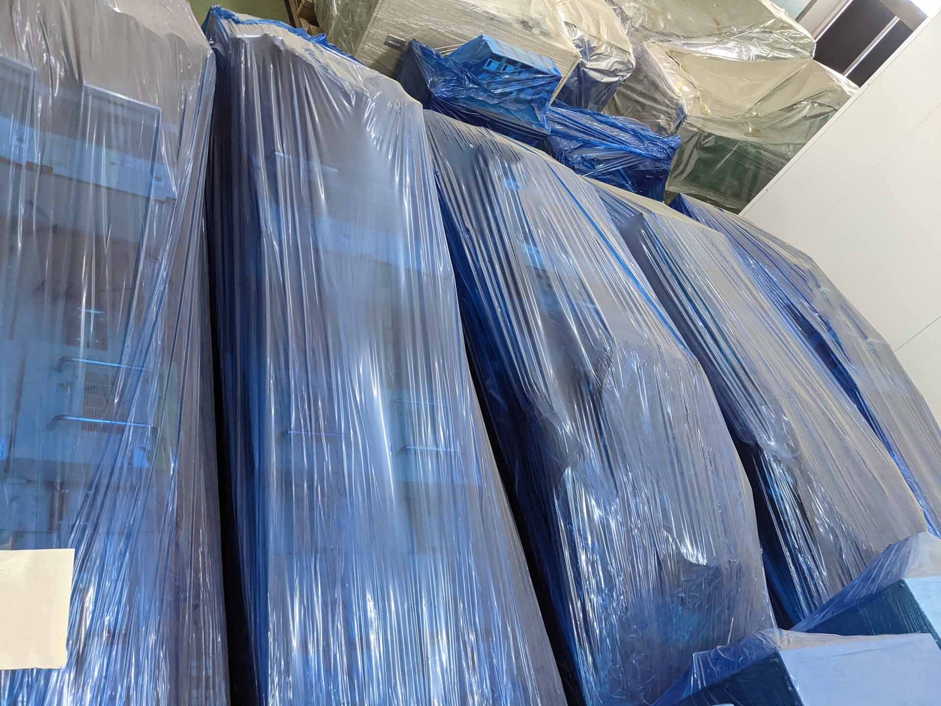

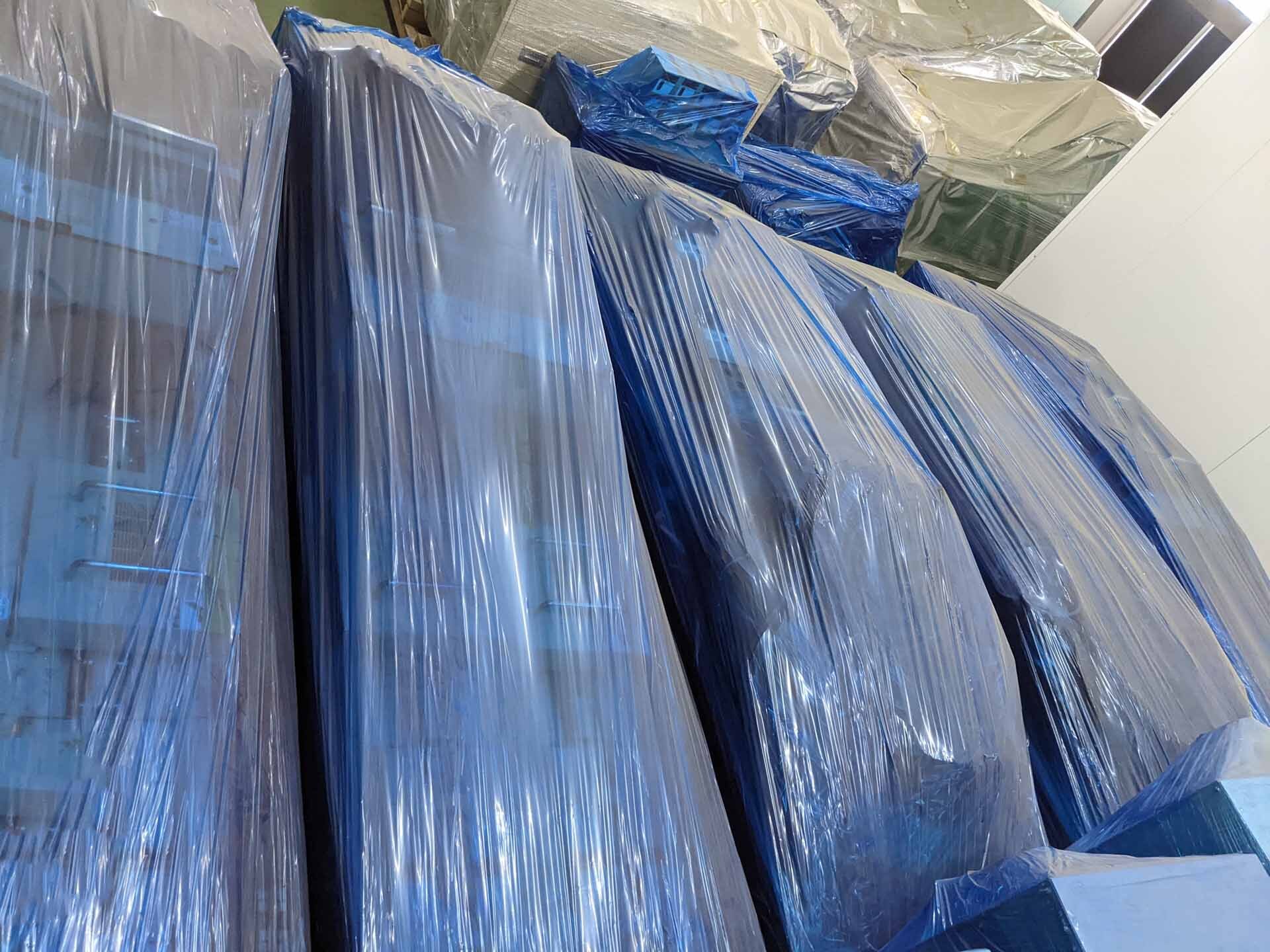
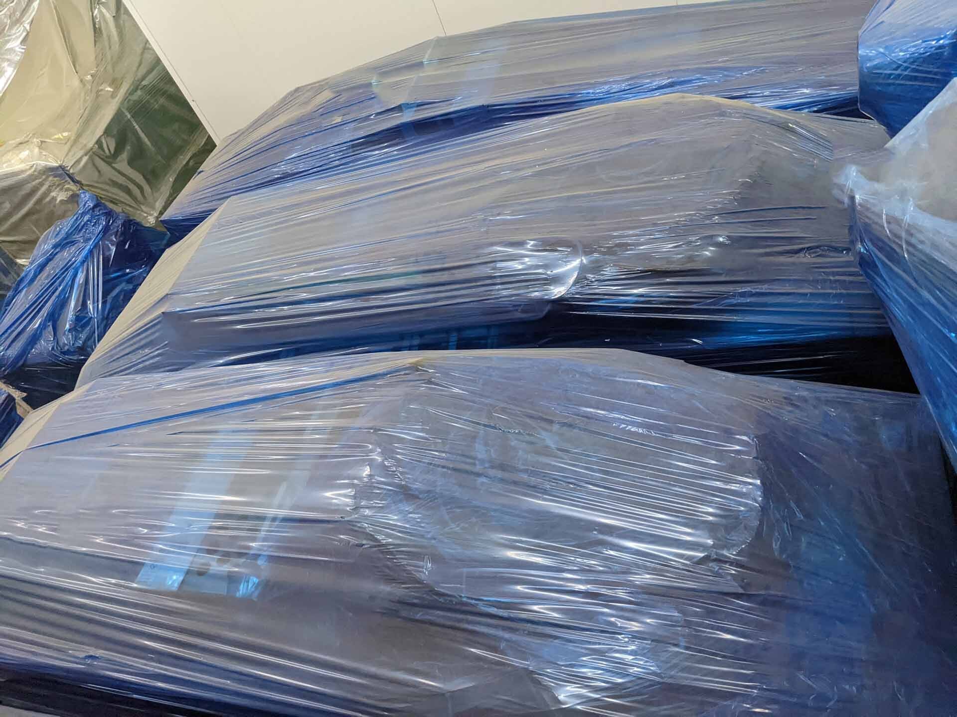
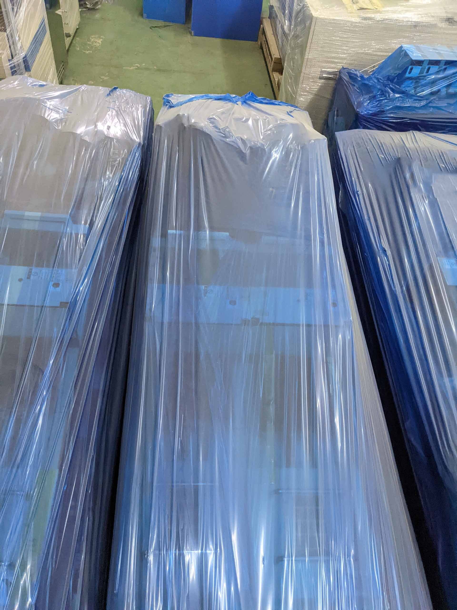
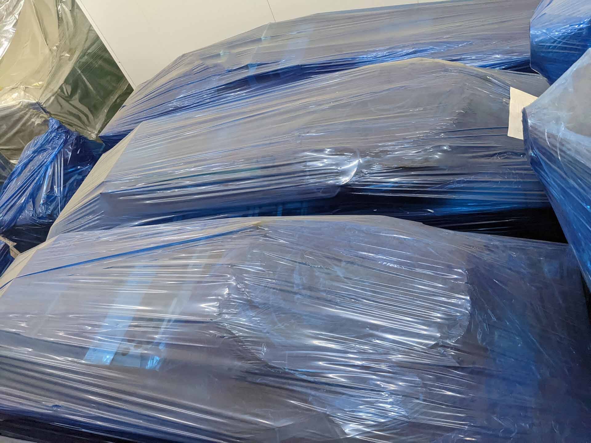
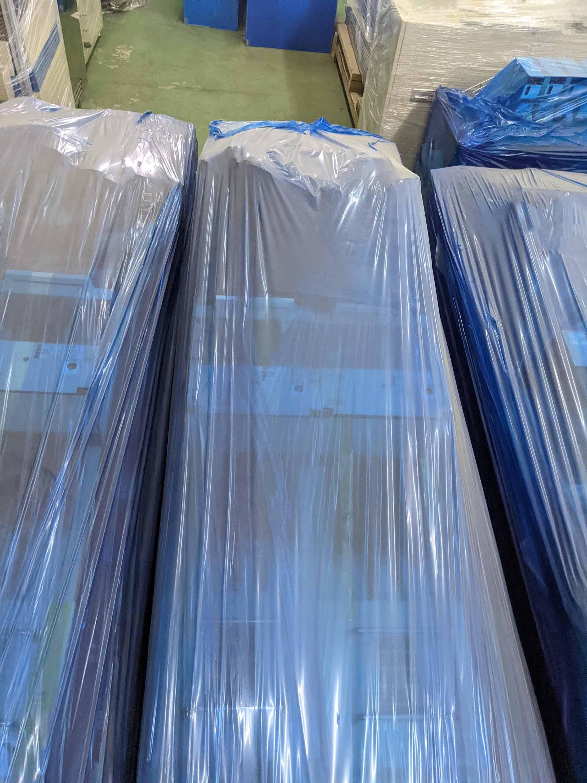
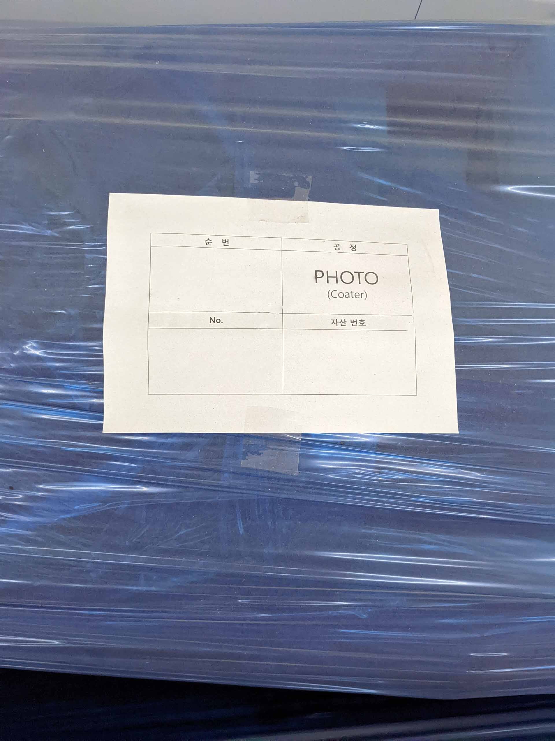
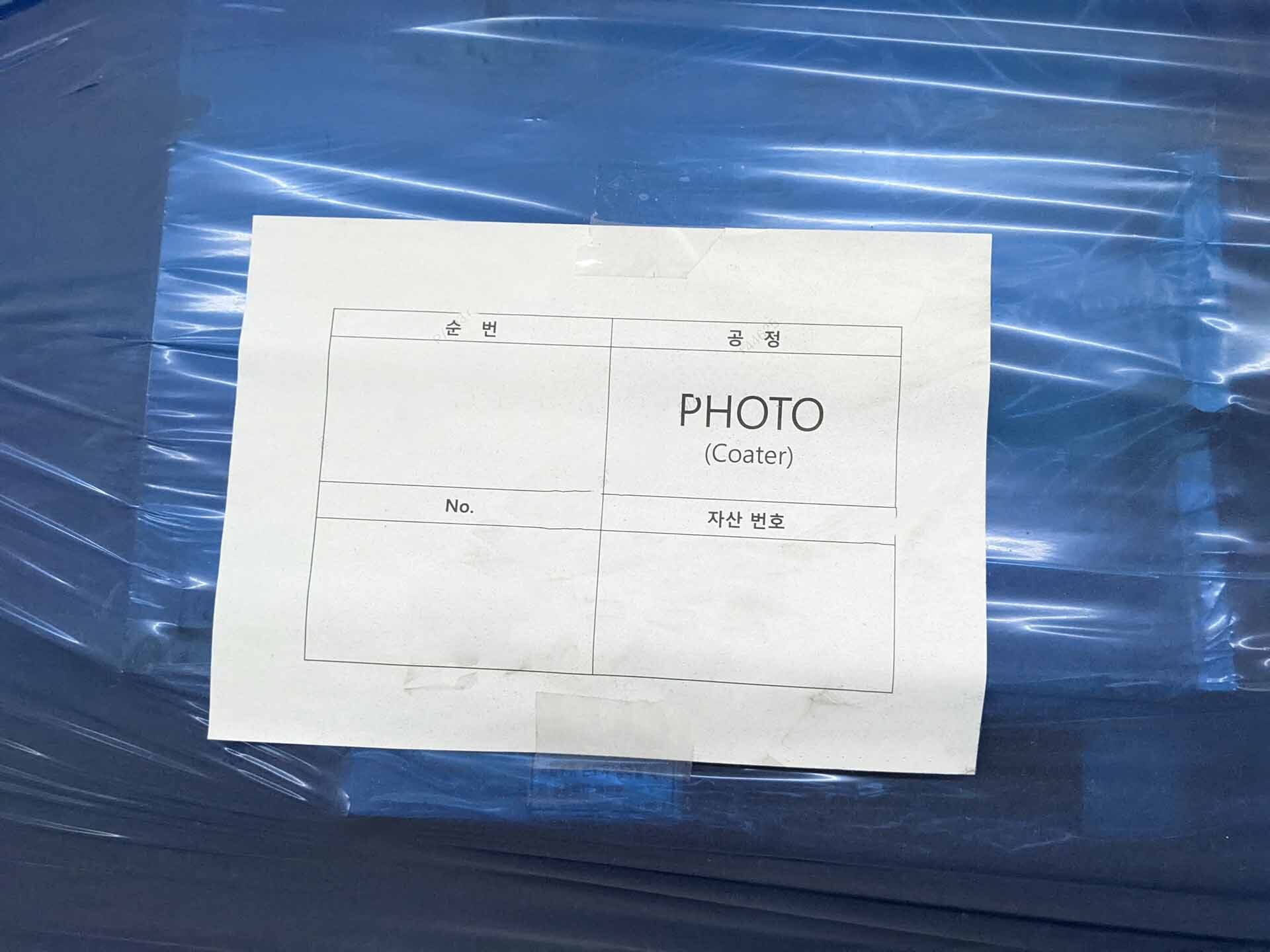
TEL / TOKYO ELECTRON MARK II equipment is a state-of-the-art, high-performance photoresist processing system designed for advanced semiconductor fabrication processes. This unit plays a crucial role in the photolithography process, which is a key step in creating semiconductor devices. TEL MARK II machine is known for its precision, reliability, and advanced capabilities that enable manufacturers to achieve high-resolution patterning for integrated circuits and other advanced electronic devices. At the heart of TOKYO ELECTRON MARK II tool is its sophisticated photoresist processing technology, which allows for precise patterning of semiconductor materials on silicon wafers. Photoresist is a light-sensitive material that acts as a mask for transferring intricate patterns onto the wafer surface during the photolithography process. MARK II asset integrates various components and subsystems to apply, expose, develop, and remove photoresist layers with utmost accuracy and consistency. One of the key features of TEL / TOKYO ELECTRON MARK II model is its advanced coating and developing capabilities. The equipment is equipped with precision coating modules that ensure uniform deposition of photoresist materials on the wafer surface. This is essential for achieving high-resolution patterns with minimal defects. TEL MARK II system also includes advanced developing chambers that effectively remove excess photoresist after exposure, maintaining the integrity of the pattern. In terms of exposure capabilities, TOKYO ELECTRON MARK II unit is equipped with advanced light sources and optical systems that allow for high-resolution patterning with sub-micron precision. The machine's alignment and registration features ensure that the patterns are accurately transferred onto the wafer surface, meeting the stringent requirements of modern semiconductor manufacturing processes. Additionally, MARK II tool offers programmable exposure parameters to accommodate various patterning requirements for different semiconductor devices. TEL / TOKYO ELECTRON MARK II asset is designed for high-throughput production environments, allowing manufacturers to achieve efficient and cost-effective semiconductor fabrication. The model's automation capabilities enable seamless wafer handling, processing, and monitoring, minimizing downtime and maximizing productivity. Additionally, TEL MARK II equipment is designed for ease of maintenance and serviceability, ensuring optimal uptime and reliability for continuous production operations. In terms of process control and monitoring, TOKYO ELECTRON MARK II system is equipped with advanced software and control systems that provide real-time feedback and data analysis. This allows manufacturers to fine-tune process parameters, optimize performance, and ensure consistent patterning quality across wafers. The unit's advanced metrology capabilities enable precise measurement and characterization of pattern features, ensuring compliance with industry standards and specifications. Overall, MARK II machine represents the cutting edge of photoresist processing technology for semiconductor fabrication. Its advanced capabilities, precision engineering, and reliability make it a preferred choice for manufacturers seeking high-performance solutions for advanced semiconductor devices. By leveraging TEL / TOKYO ELECTRON MARK II tool, manufacturers can achieve high-resolution patterning, improved process control, and enhanced productivity in semiconductor fabrication applications.
There are no reviews yet