Used TEL / TOKYO ELECTRON MARK II #293700416 for sale
URL successfully copied!

























Tap to zoom
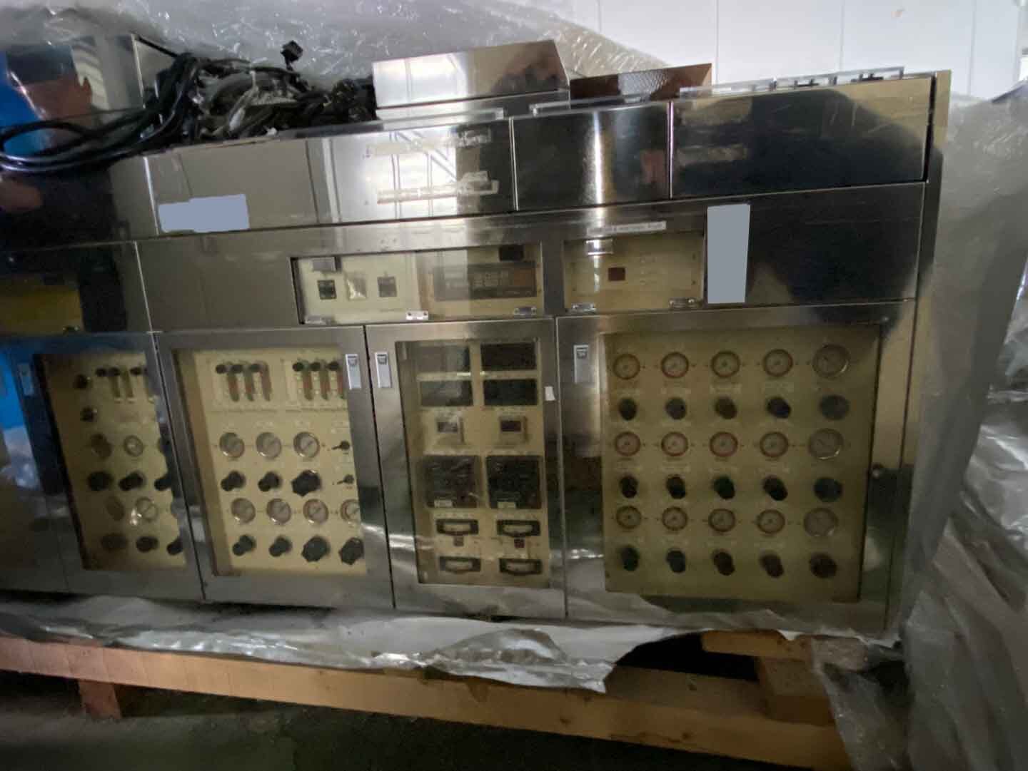

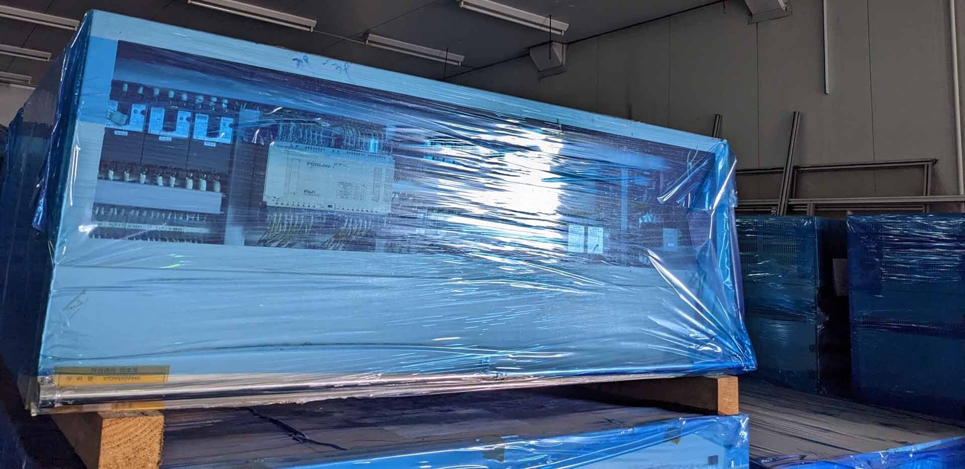
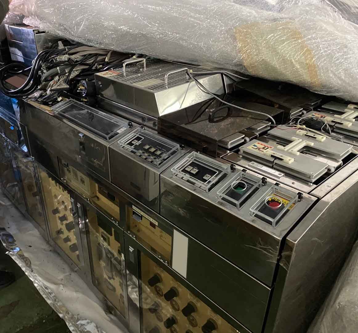
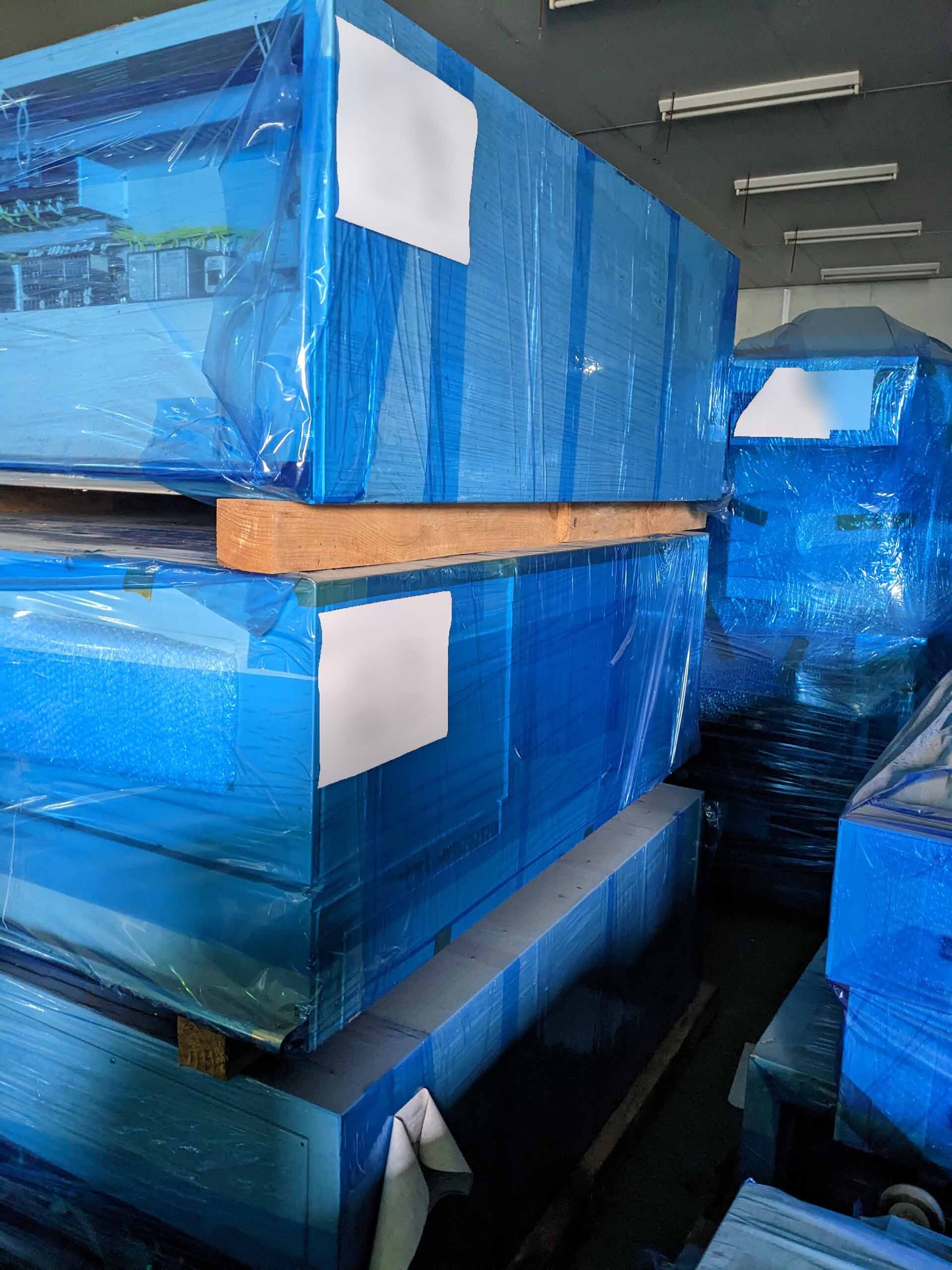
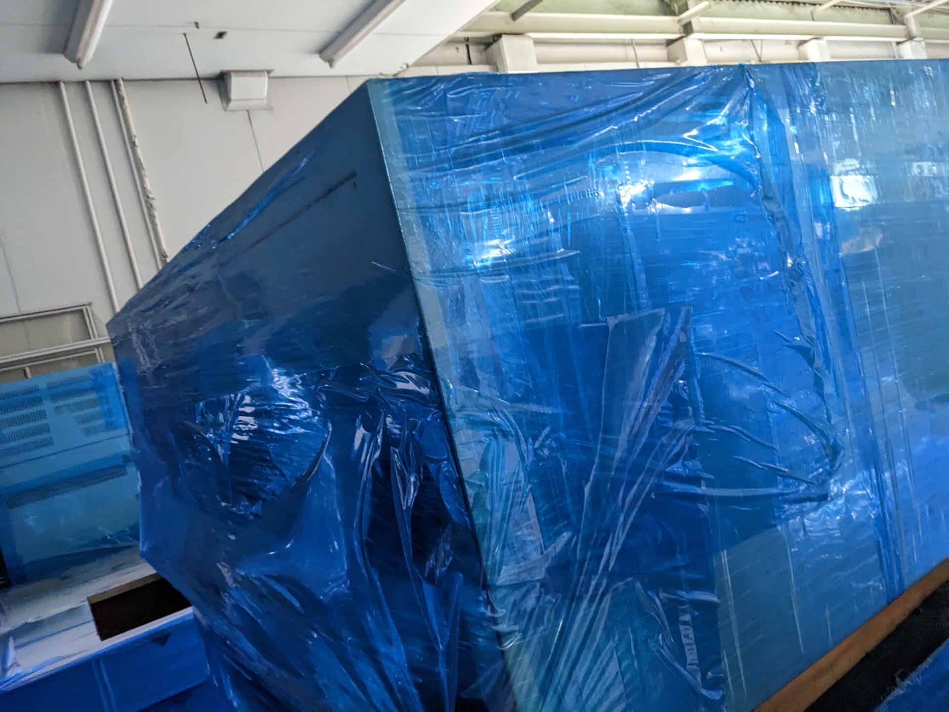

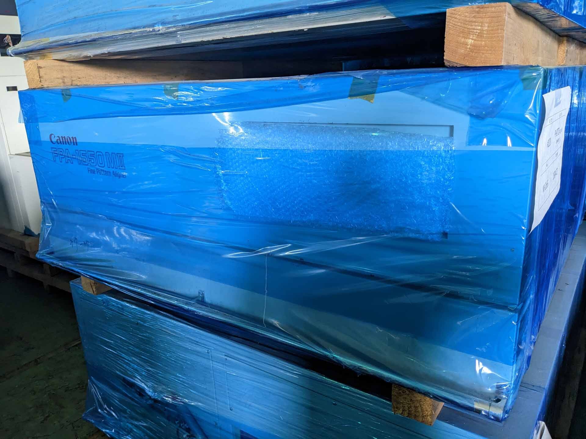
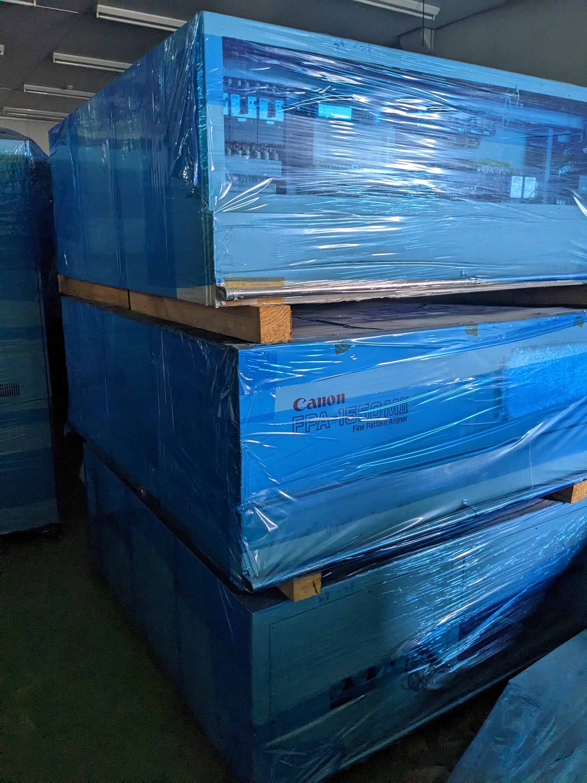
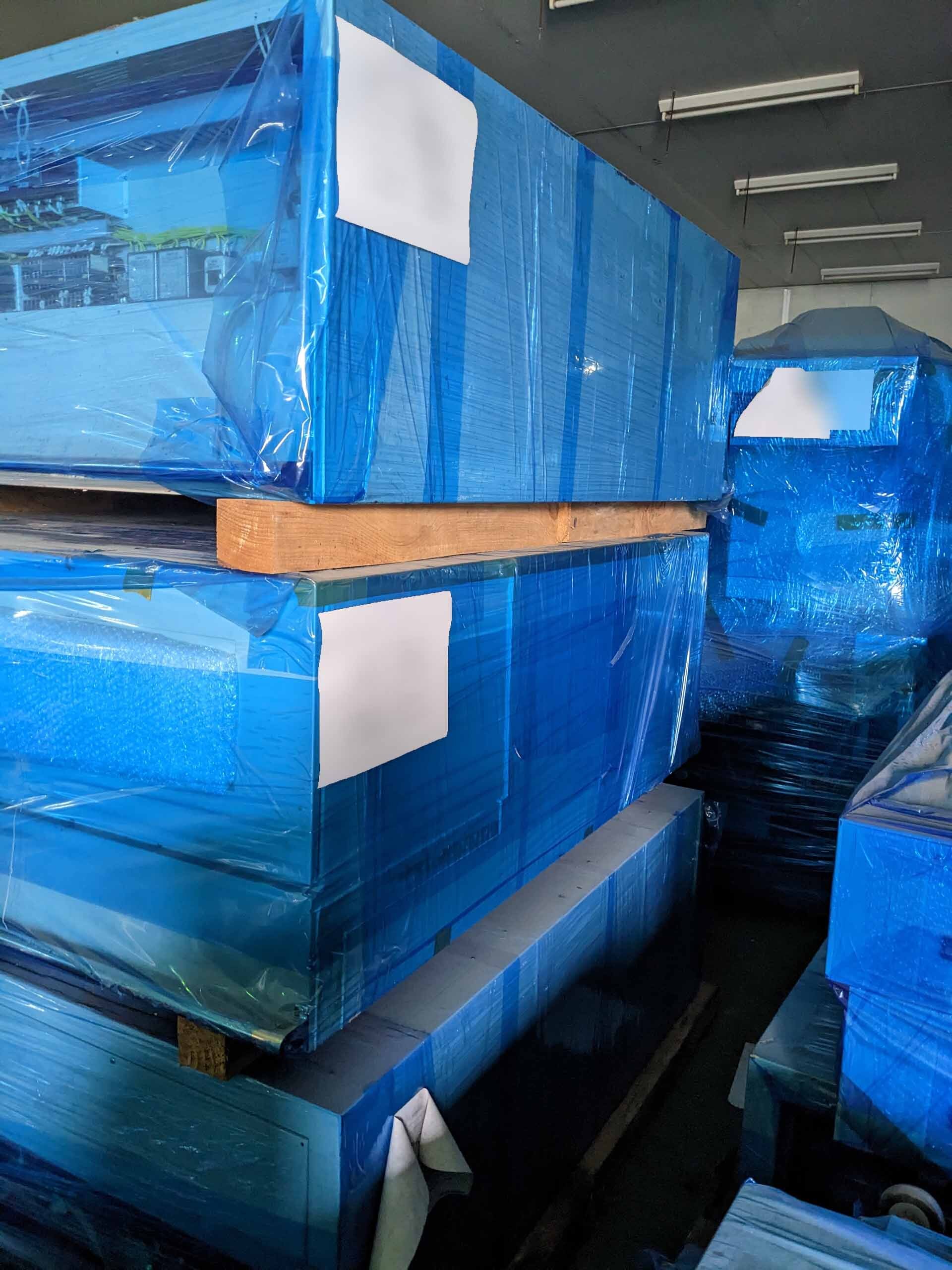
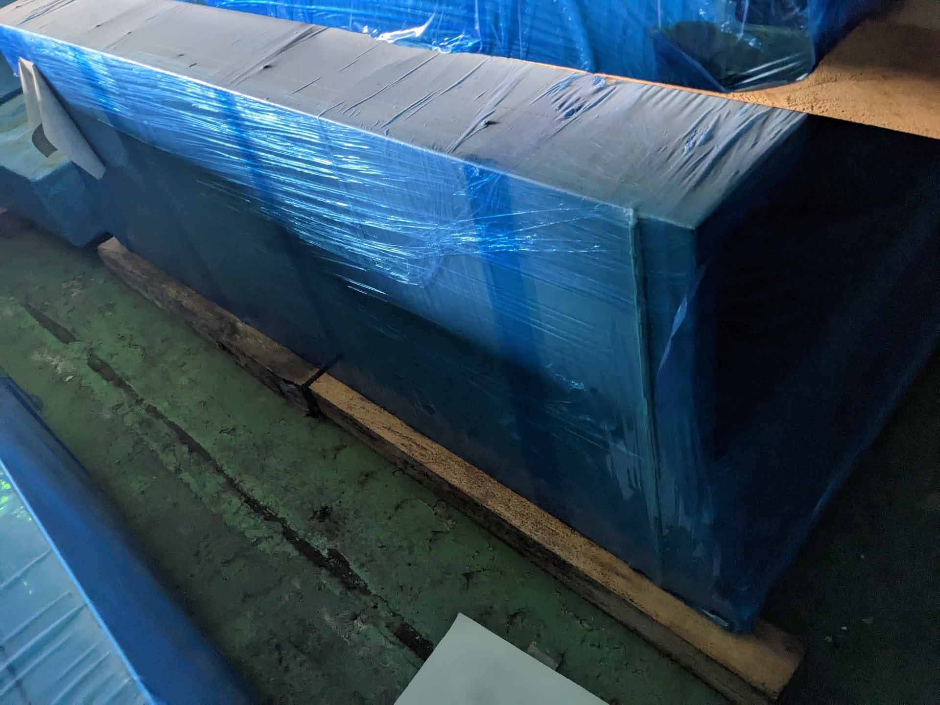
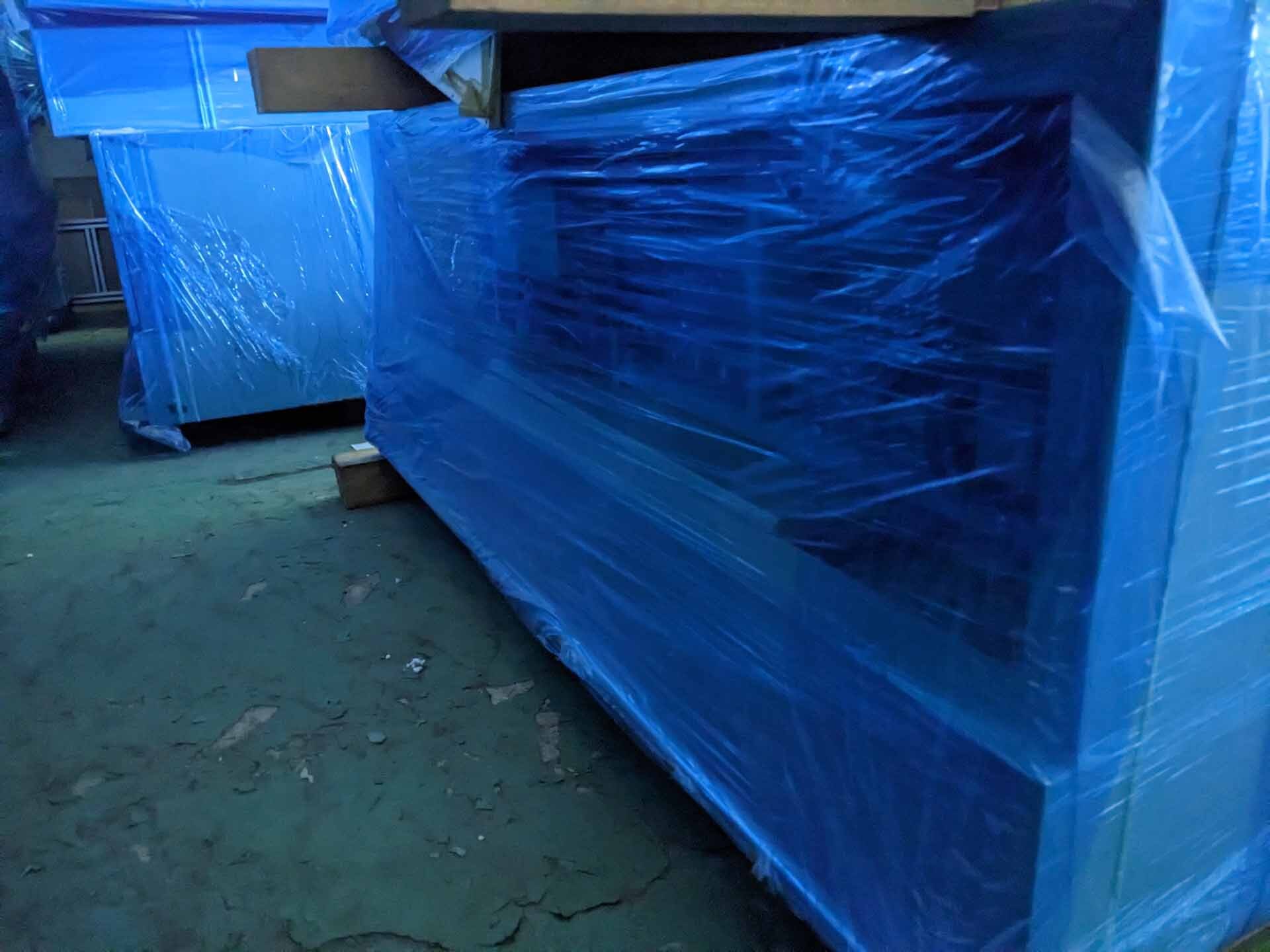
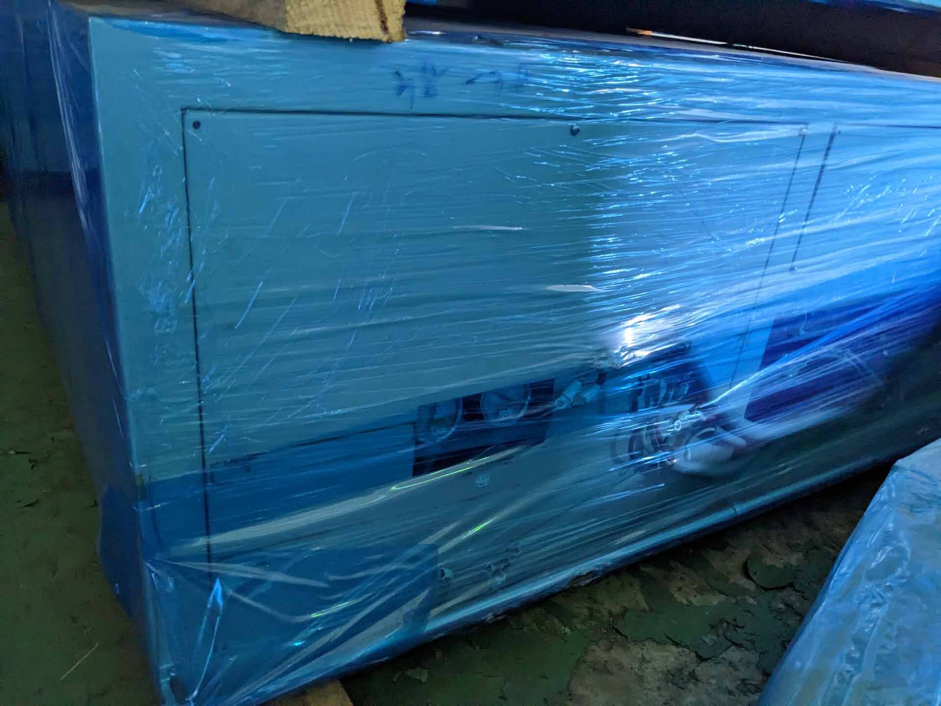
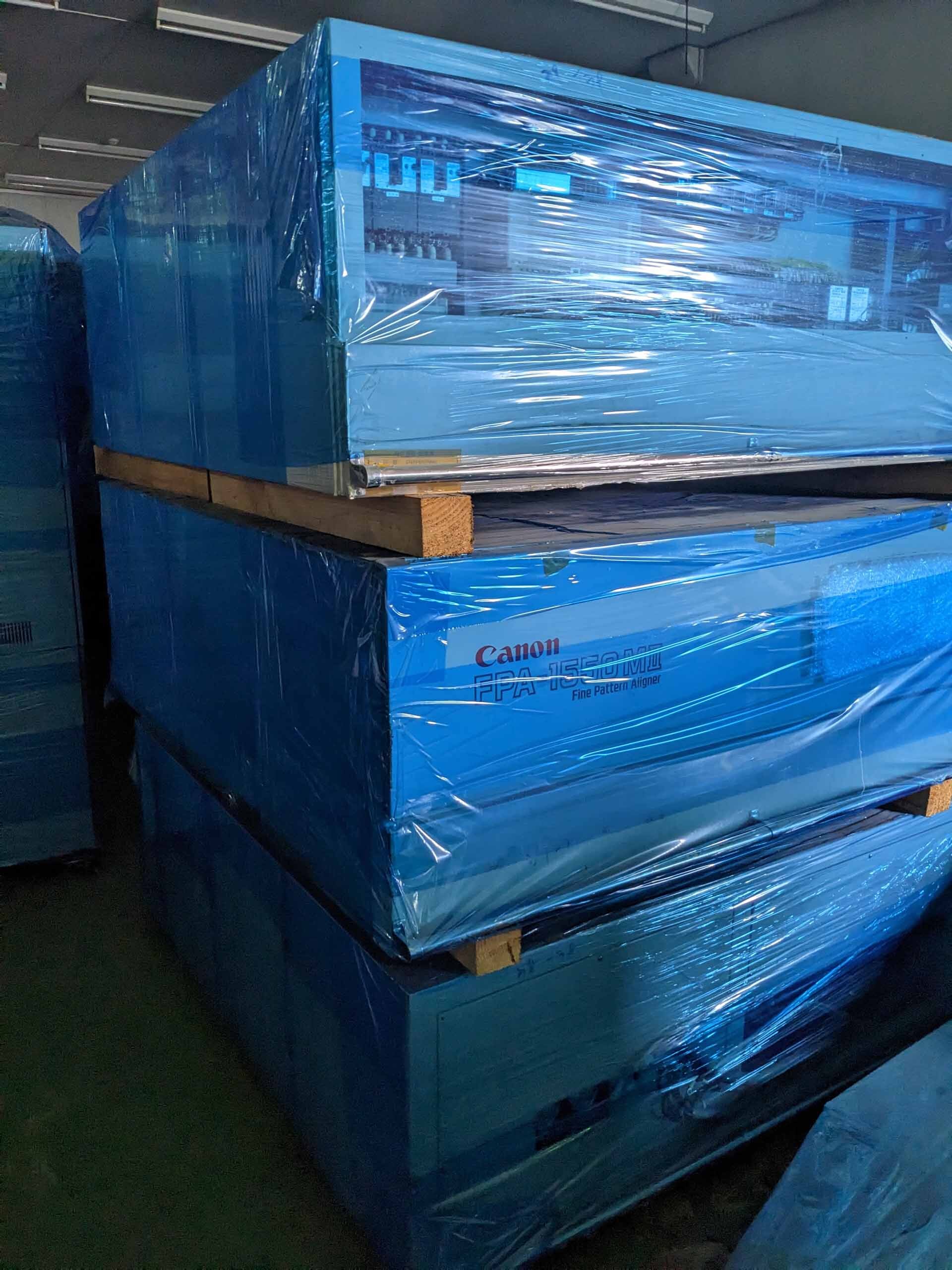

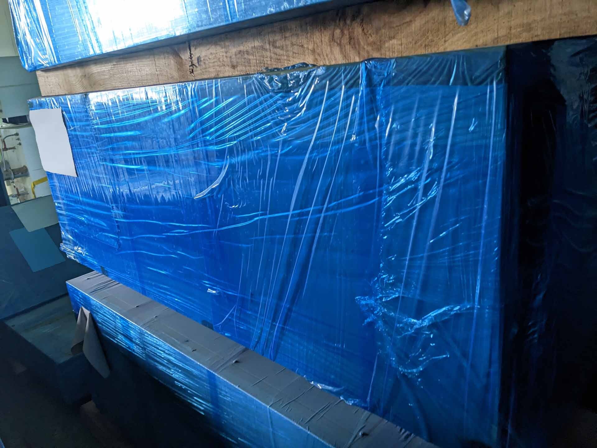
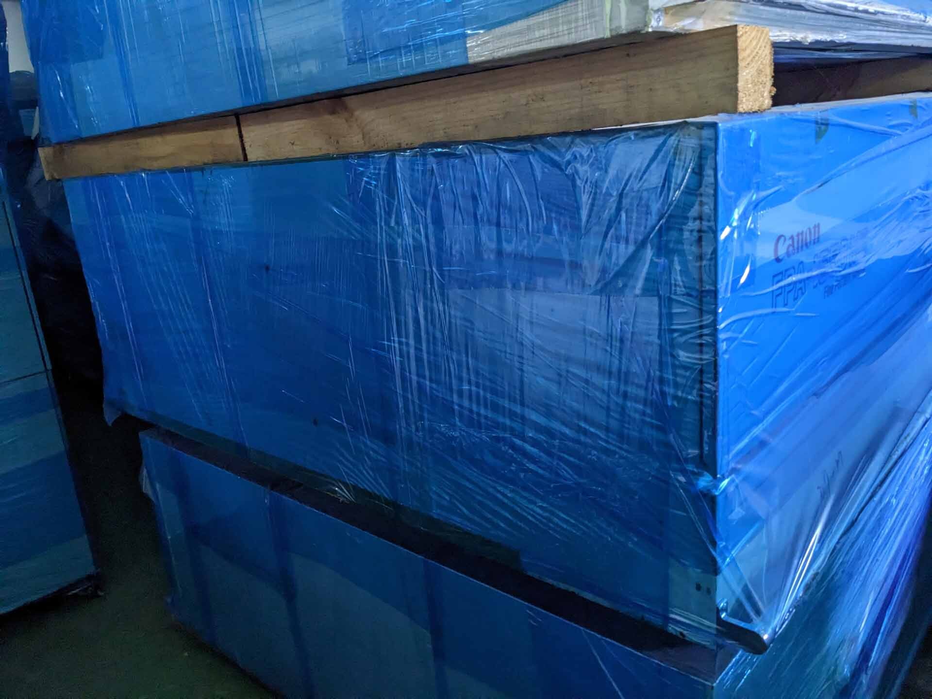
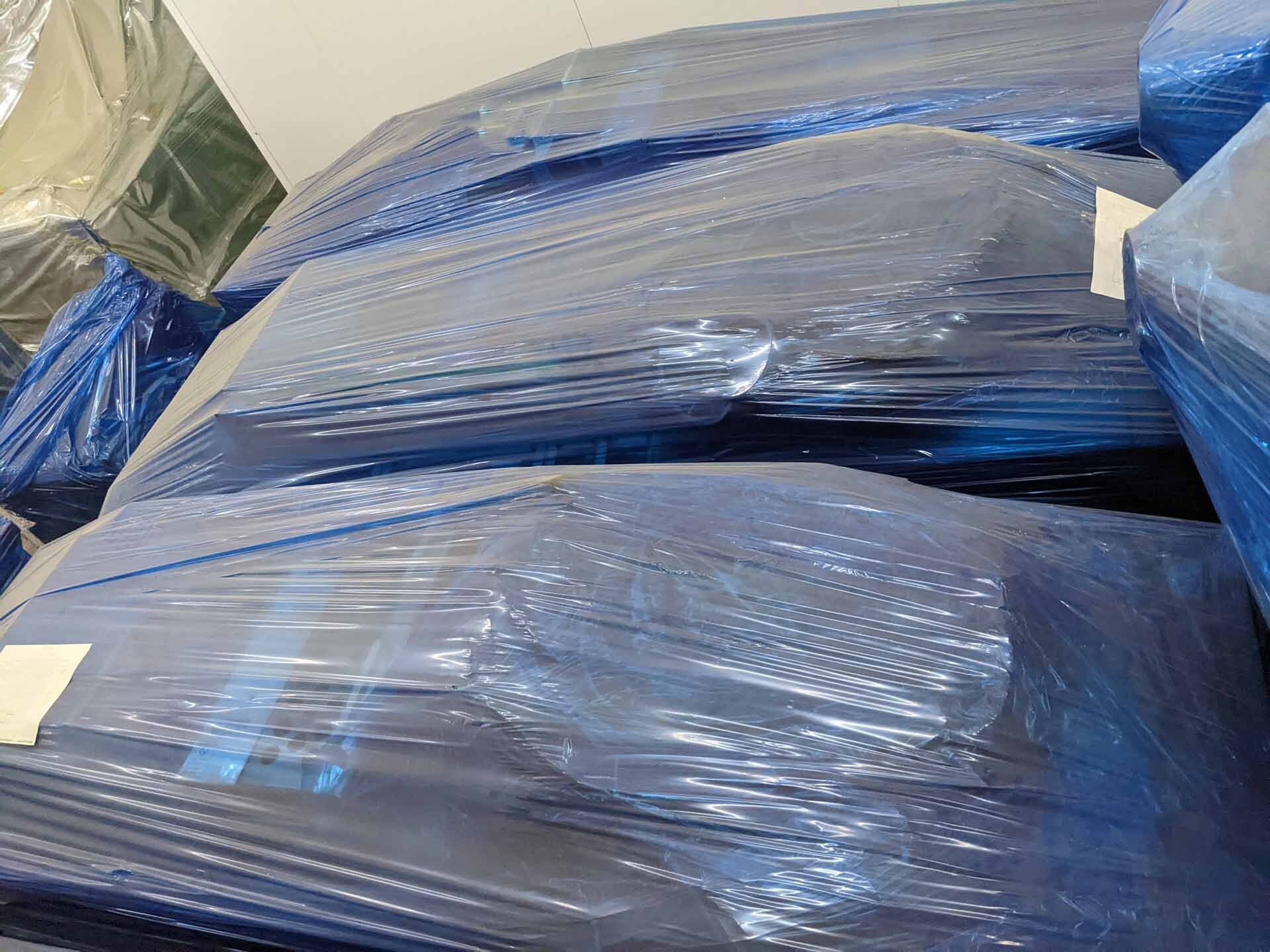
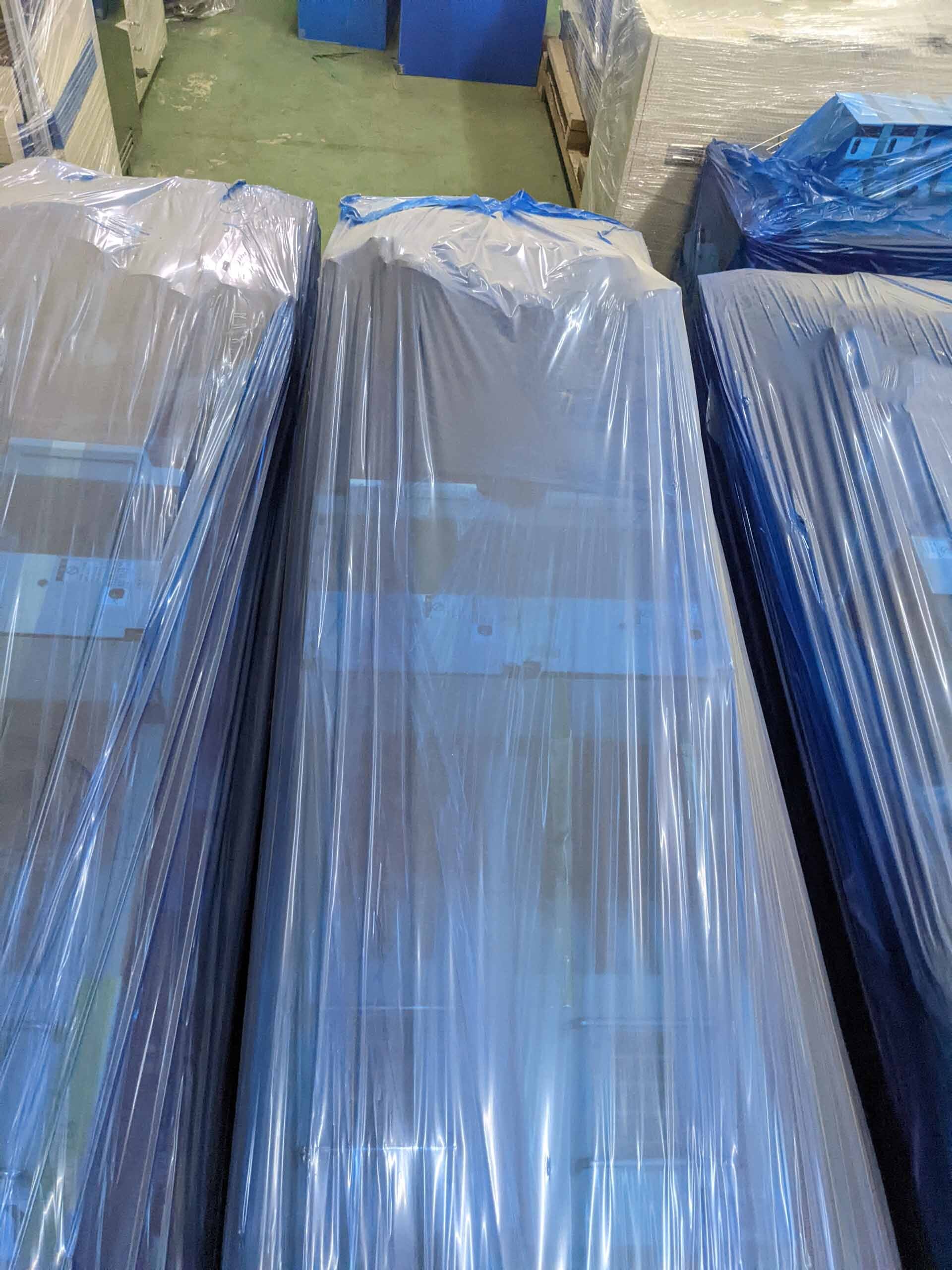
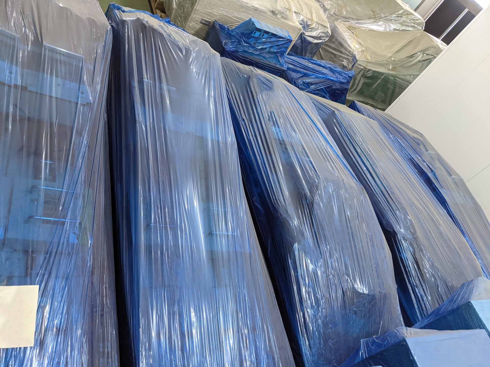
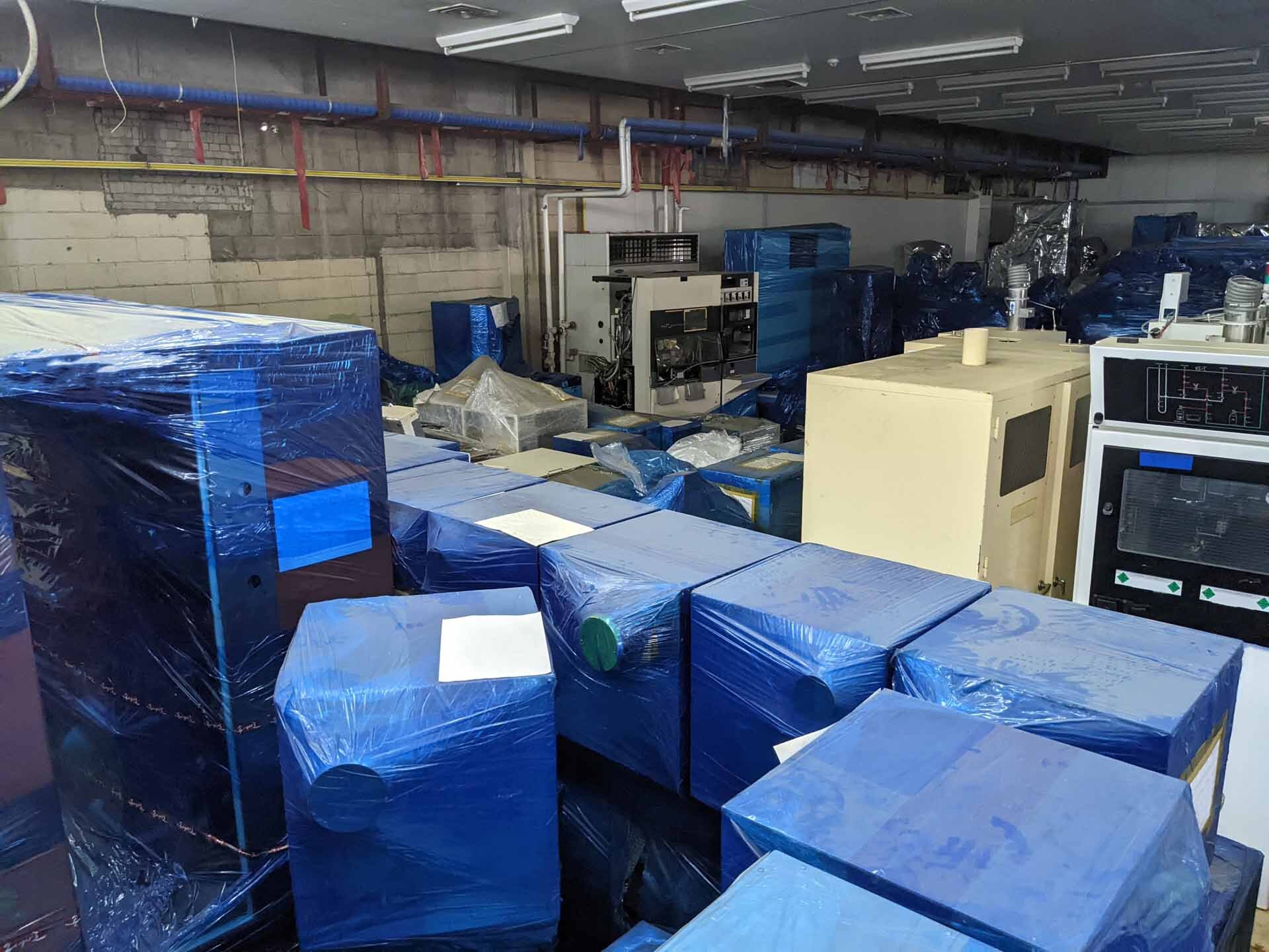
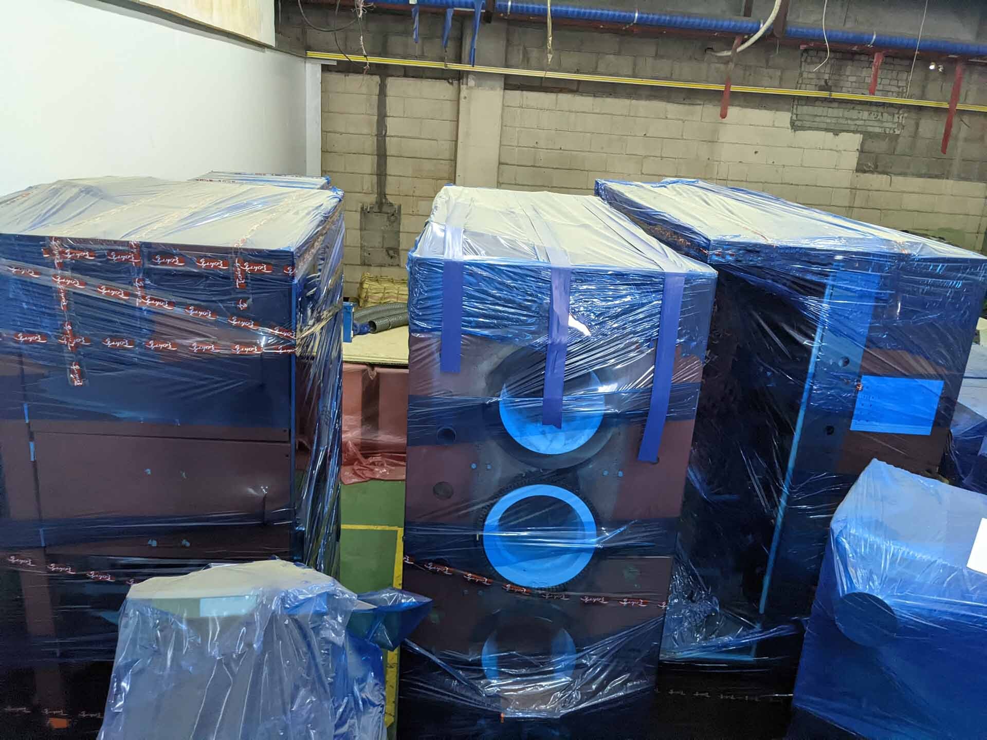
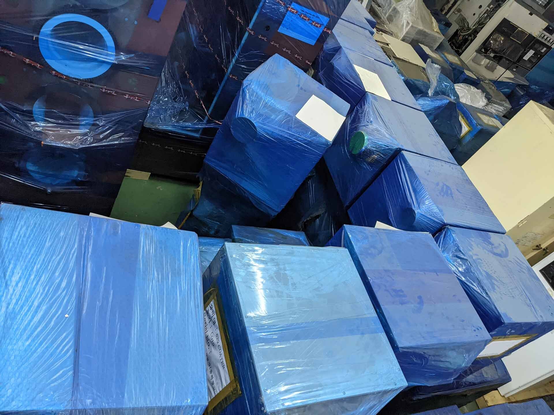
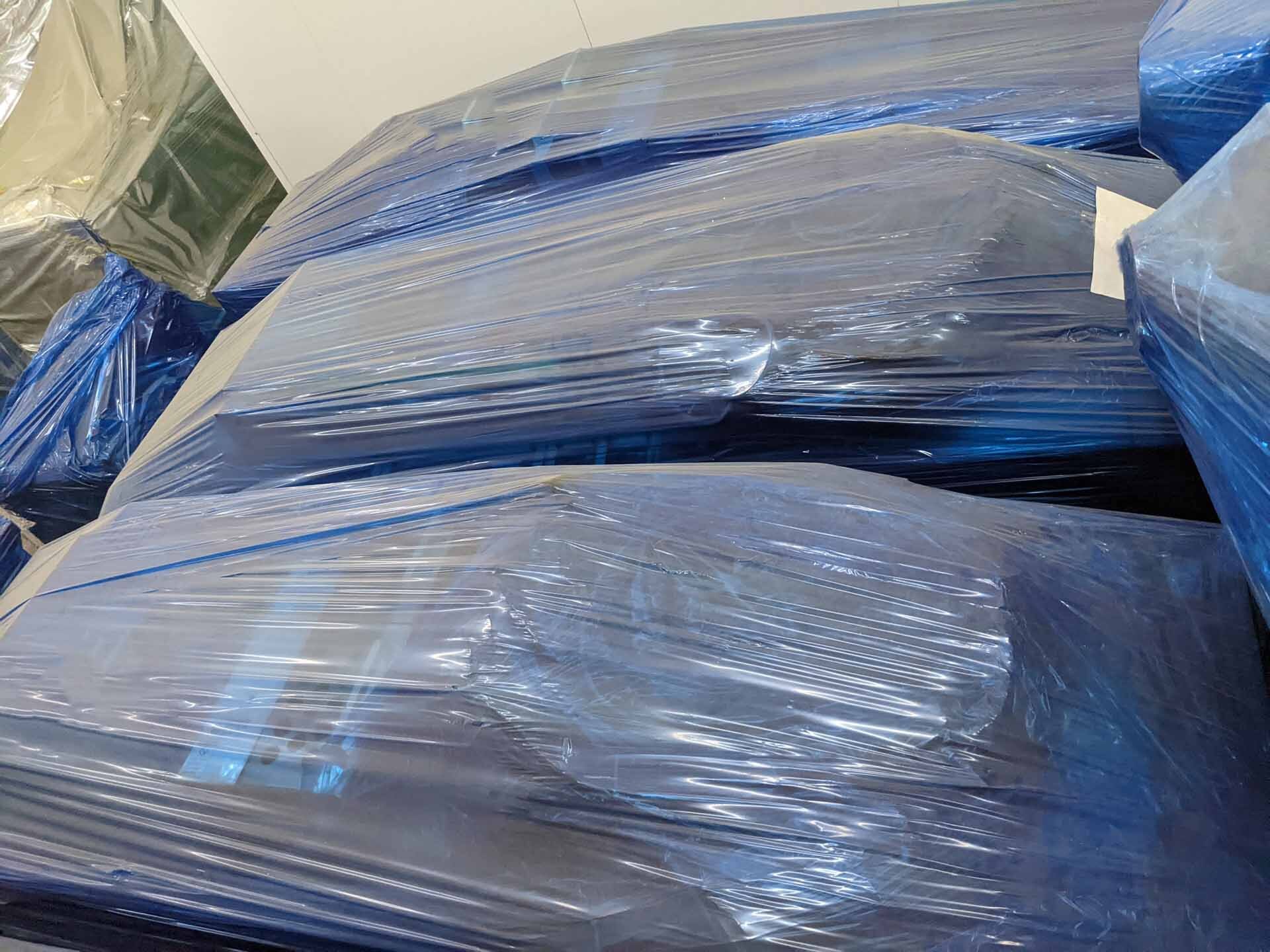
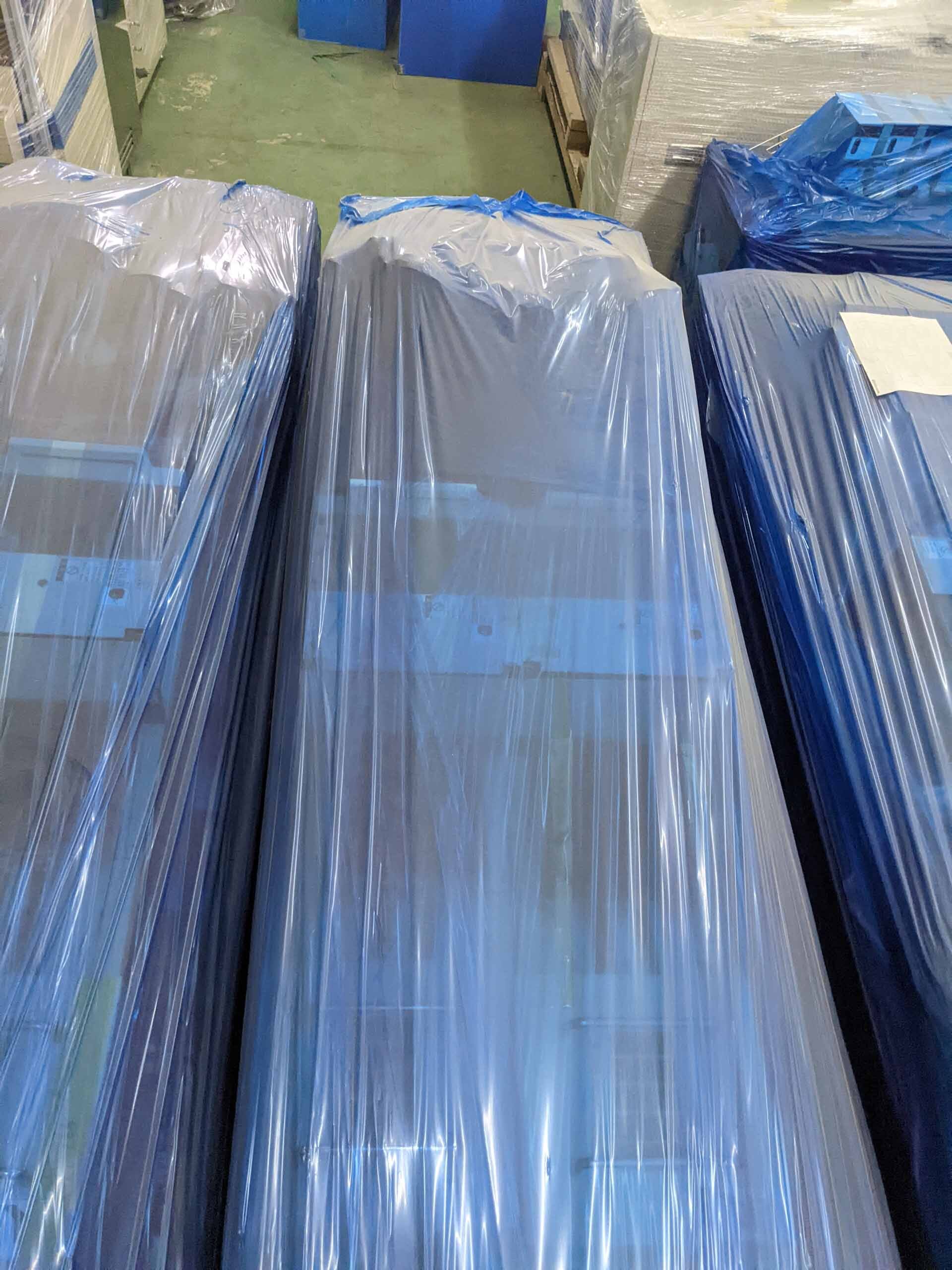
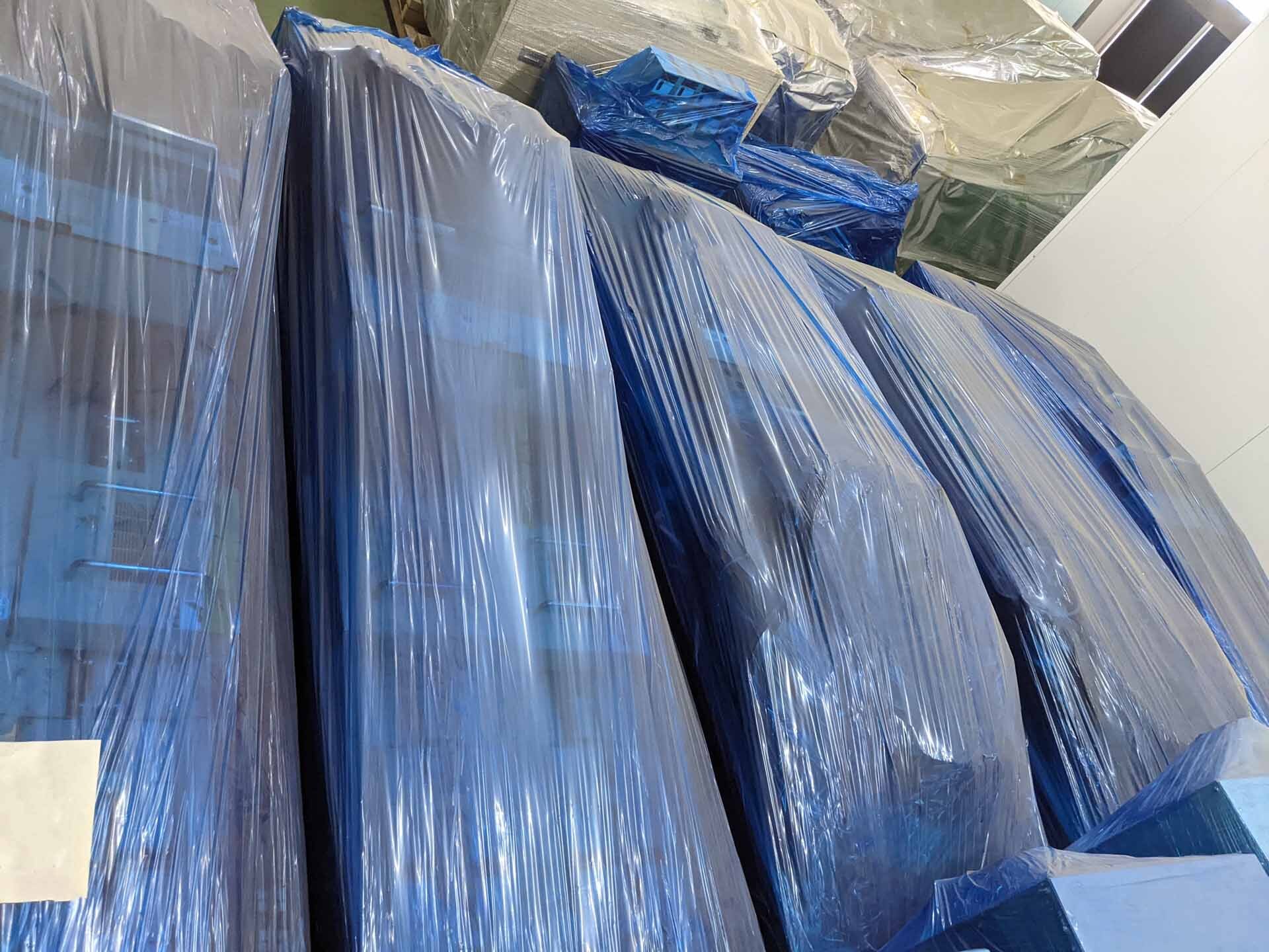
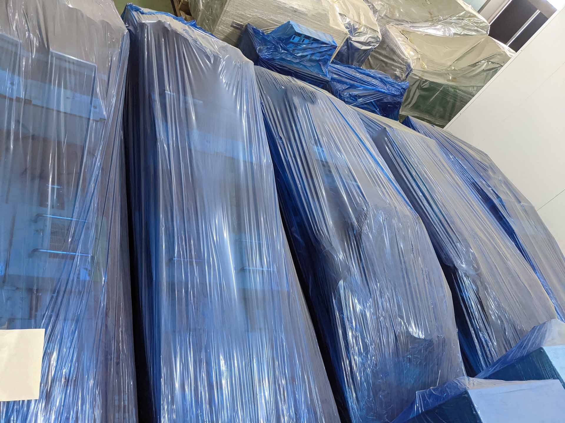
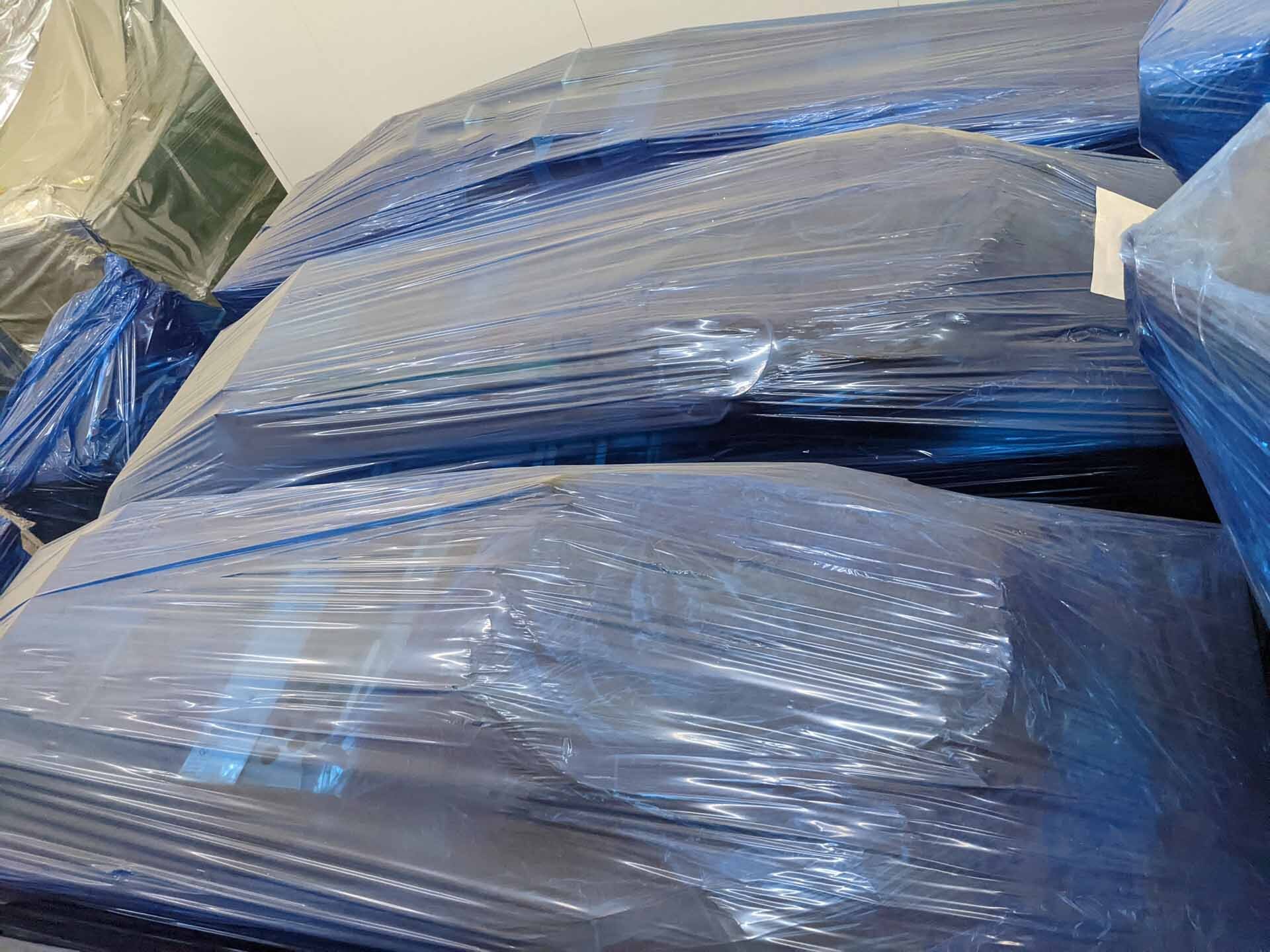
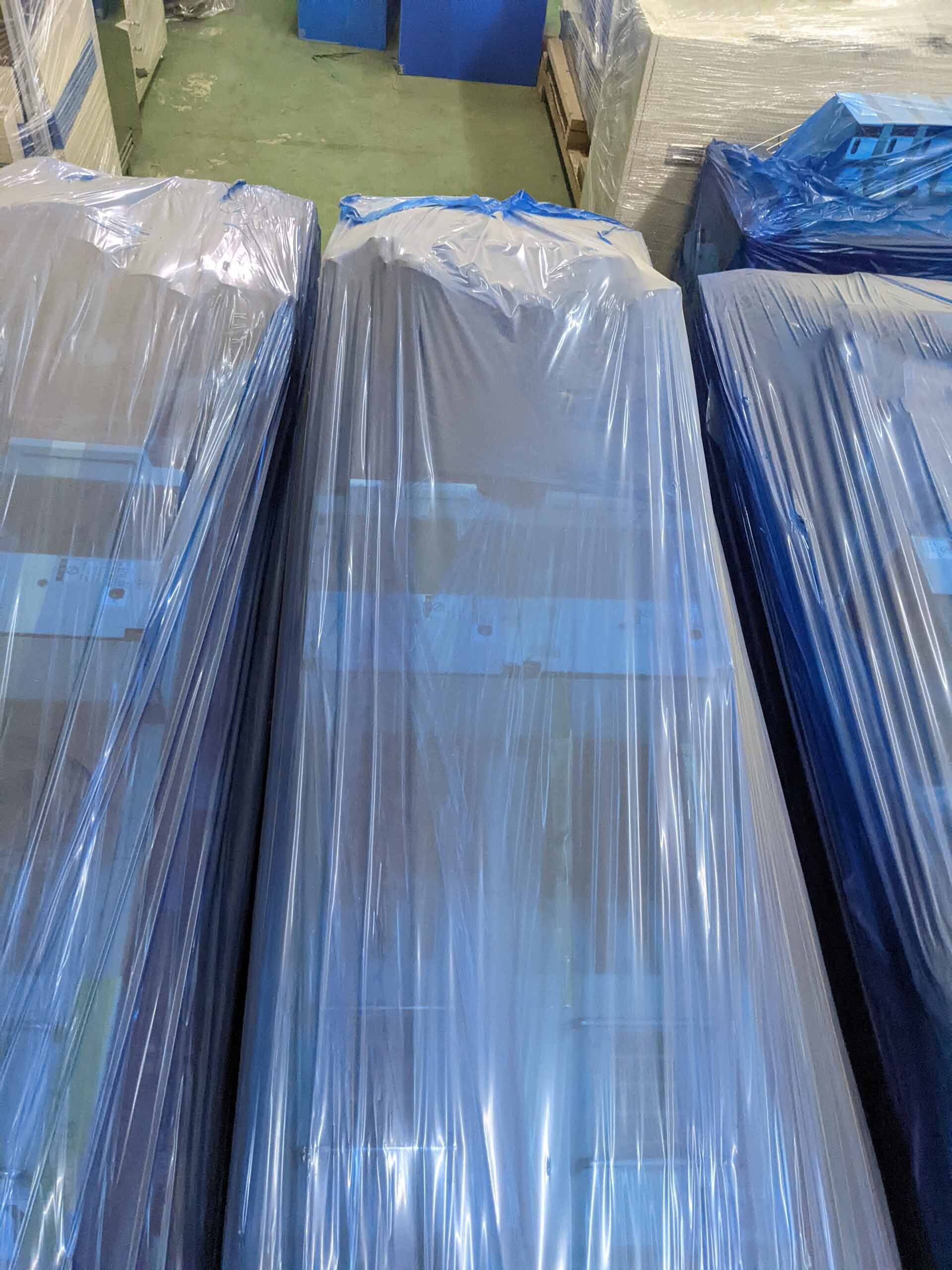
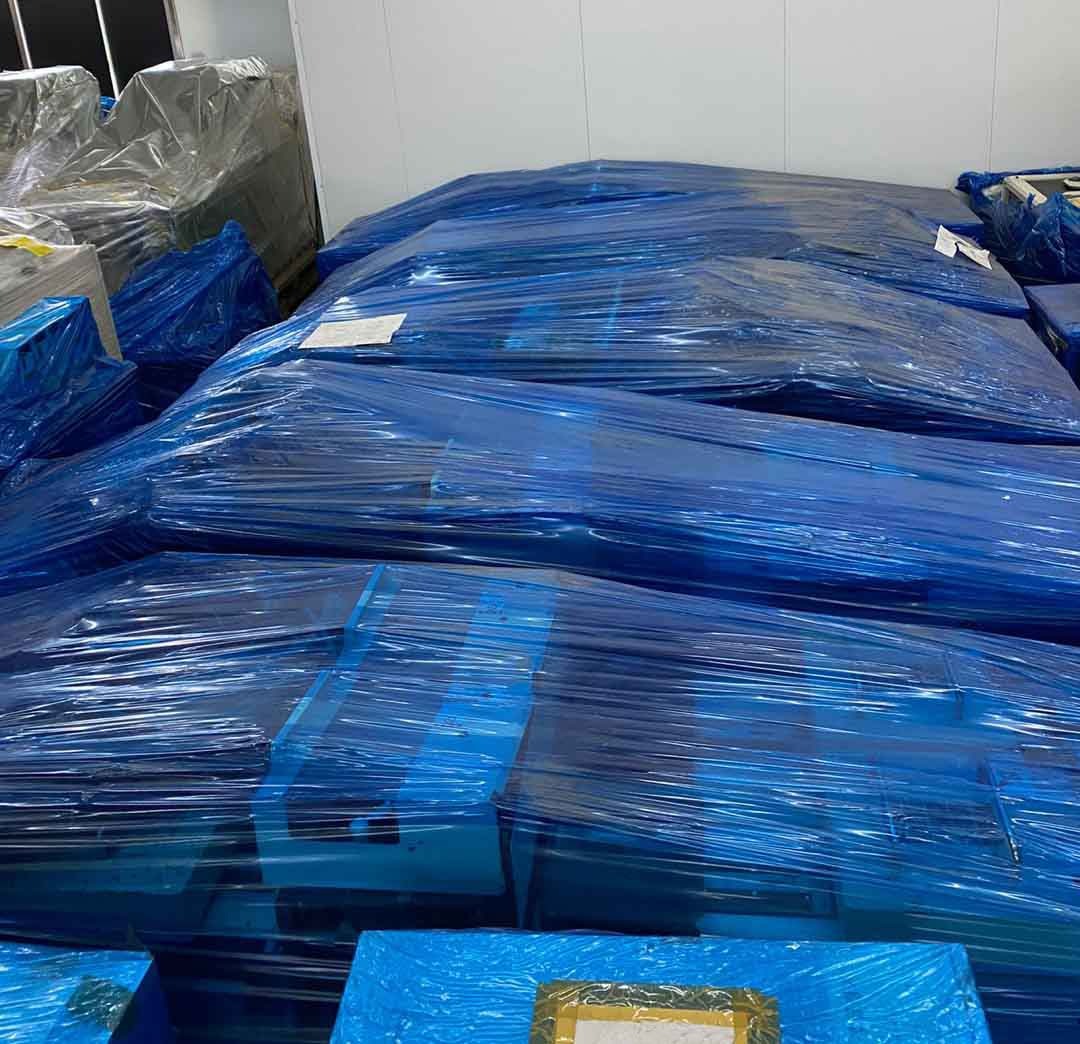
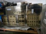
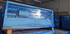
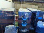
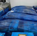
TEL / TOKYO ELECTRON MARK II is a sophisticated photoresist equipment commonly used in the semiconductor industry for precise photolithography processes. This advanced system is designed to provide high-resolution patterning on silicon wafers, enabling the creation of intricate circuit designs essential for semiconductor manufacturing. With its cutting-edge technology and specialized capabilities, TEL MARK II offers unparalleled performance and accuracy in the production of semiconductor devices. At the core of TOKYO ELECTRON MARK II unit is its photoresist application and development capabilities. Photoresist is a light-sensitive material applied to the silicon wafer surface to define patterns during the lithography process. MARK II machine uses a combination of advanced coating techniques, such as spin coating and chemical vapor deposition (CVD), to uniformly apply photoresist layers of varying thicknesses onto the wafer surface. This precise control over the photoresist deposition ensures consistent and repeatable patterning results across the wafer. One of the key features of TEL / TOKYO ELECTRON MARK II tool is its multi-stage heating and baking capabilities for photoresist curing. After the photoresist is applied to the wafer, it needs to undergo a series of heating and baking steps to remove solvents and improve adhesion to the wafer surface. TEL MARK II asset incorporates programmable heating profiles and controlled environments to optimize the curing process and enhance the overall quality of the patterned features. In addition to photoresist application and curing, TOKYO ELECTRON MARK II model also includes advanced patterning tools for photolithography. These tools typically consist of a high-resolution exposure equipment, such as a stepper or scanner, capable of projecting patterns onto the wafer with micron-scale accuracy. MARK II system leverages state-of-the-art optics, alignment systems, and light sources to ensure precise pattern transfer onto the photoresist-coated wafer surface. Furthermore, TEL / TOKYO ELECTRON MARK II unit offers advanced control and automation features to streamline the lithography process and minimize human error. The machine is equipped with sophisticated software algorithms for mask alignment, exposure dose control, and critical dimension measurement, allowing for real-time monitoring and adjustment of lithography parameters. This level of automation ensures consistent patterning results and reduces cycle time in semiconductor fabrication. Overall, TEL MARK II photoresist tool represents a pinnacle of technology in semiconductor lithography, offering unmatched precision, reliability, and efficiency in the production of advanced semiconductor devices. By incorporating cutting-edge coating, curing, and patterning capabilities, this asset enables semiconductor manufacturers to achieve sub-micron resolution and complex geometries required for next-generation integrated circuits. With its comprehensive set of features and advanced performance metrics, TOKYO ELECTRON MARK II model is a crucial tool in the semiconductor industry for achieving high-quality lithography results and driving innovation in semiconductor device design and manufacturing processes.
There are no reviews yet