Used TEL / TOKYO ELECTRON Mark V #149605 for sale
URL successfully copied!
Tap to zoom


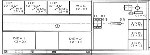
TEL / TOKYO ELECTRON Mark V photoresist equipment is a next-generation photolithography system designed with the latest in optical design, microfabrication and semiconductor processing technology. TEL Mark V is capable of reproducing patterns with superior accuracy and repeatability on microcomponents, ideal for those involved in semiconductor chip and microchip manufacturing. Developed by TEL Ltd., TOKYO ELECTRON MARK-V is a dedicated unit used to apply photoresists onto semiconductor wafers. Photoresist refers to a material that can be selectively removed by exposure to radiant energy, making it an essential material used in semiconductor manufacturing. TEL MARK-V machine utilizes this specialty material to create circuit patterns with amazing precision and repeatability. TOKYO ELECTRON Mark V tool is capable of reproducing complex patterns on extremely small scales with a wide variety of photoresist materials and can also effectively spin coat larger wafers. MARK-V's features include a high-precision stage, a programmable translating table and an advanced optical asset. The carousel-style stage is capable of accommodating wafers up to 4 inches in diameter. The four stepper motor-driven table can be programmed with multiple recipes and auto repeatable moves used to accurately place components and materials. To further ensure accuracy, TEL / TOKYO ELECTRON MARK-V utilizes a newly-developed beam model with a highly-stable laser. The laser beam is efficiently delivered to the workpiece via a cat's-eye lens array and optical fibers. To reduce the time required for production, Mark V is capable of running multiple identical recipes at the same time, offering high throughput and reduced process time. Cleaning is accomplished via TEL / TOKYO ELECTRON Mark V's on-board high-end EPC (Electrostatic Precipitation Cleaner) and a vacuum chuck equipment with a standard chemical-resistant nozzle. TEL Mark V is an advanced photoresist system for micro components that is highly capable and ultra-precise. With its powerful features, high throughput capabilities and advanced optical design, this next-generation unit is designed to ensure the best possible accuracy and repeatability on semiconductor chip and microchip components.
There are no reviews yet