Used TEL / TOKYO ELECTRON Mark V #293759024 for sale
URL successfully copied!



Tap to zoom
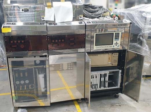

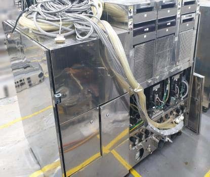
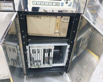
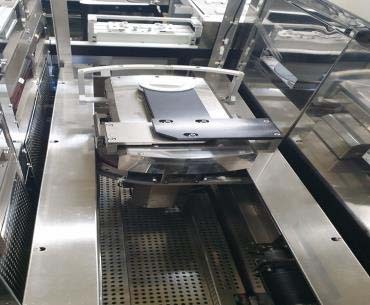
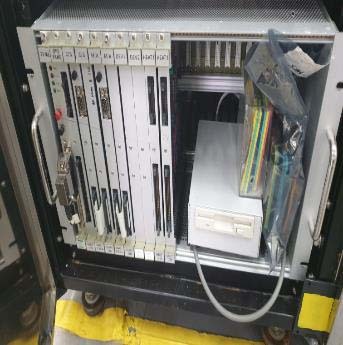
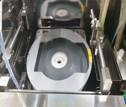
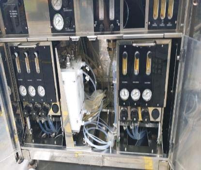
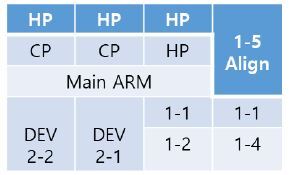
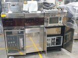
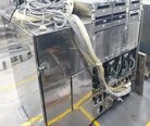
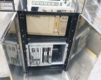
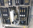
TEL / TOKYO ELECTRON Mark V is a photoresist equipment that is used in semiconductor production operations to produce patterns on wafers during the photolithography process. TEL Mark V photoresist system is part of the suite of products available from TEL, and is used primarily for maskless lithography and development operations. TOKYO ELECTRON MARK-V unit is equipped with a range of components and features designed to facilitate faster and more accurate exposure of photoresist to create highly precise patterns on wafers. The machine includes a high-resolution, high-precision optical imaging tool, a vacuum stage for holding the wafer during imaging, and a compact, easy to use controller unit. The optical imaging section of Mark V is designed for extremely stable, low noise performance and is capable of projecting patterns on the resist consistently and accurately. The projection optics employ an advanced laser-scanning asset which can achieve a resolution of 30nm. The wafer vacuum stage allows for very precise control of the wafer during imaging, in order to ensure that the pattern is properly aligned and perfectly centered. The controller unit of TOKYO ELECTRON Mark V model is designed to be user-friendly, making it easy to set exposure parameters and other operating parameters with minimal effort. The controller also includes several features that enable more comprehensive control, such as exposure simulation, pattern editing, and alignment calibration. This makes it possible to fine-tune the imaging process and ensure perfect accuracy. MARK-V photoresist equipment is a reliable and versatile tool for semiconductor manufacturers, especially for those who demand the highest accuracy for their photolithography operations. With its high-precision optical imaging capabilities and advanced control features, the system can produce high-quality, high-resolution patterns quickly and consistently.
There are no reviews yet