Used TEL / TOKYO ELECTRON Mark V #293759031 for sale
URL successfully copied!



Tap to zoom
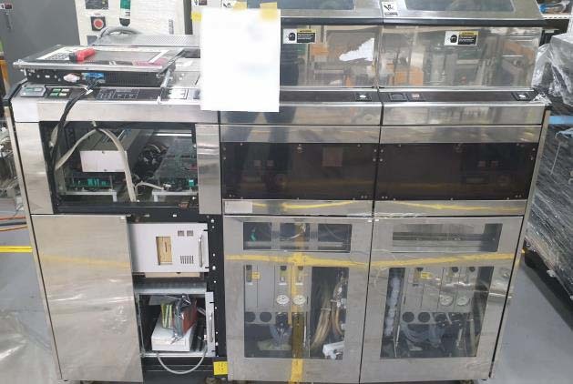

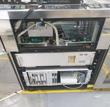
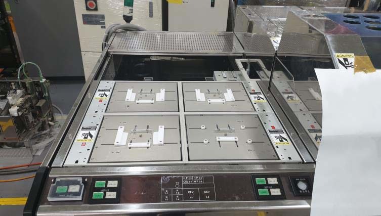
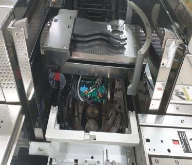
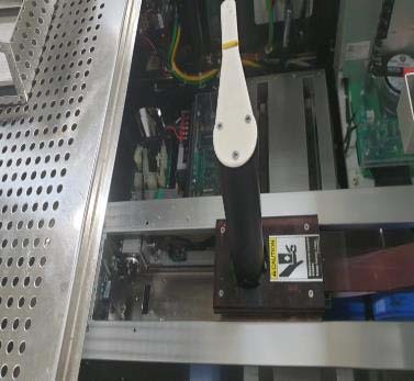
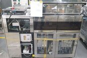
TEL / TOKYO ELECTRON Mark V is a highly advanced Photoresist Equipment designed for precise patterning of semiconductor devices. This system is capable of producing high-resolution patterns of various shapes and sizes on substrates. It is a very advanced technology that uses advanced optical systems, high-precision automated stages, and precise robotics to achieve precise alignment and registration. The unit is highly precise, with a positional repeatability of 0.5 microns, lapping accuracy of 0.5 microns and tilt accuracy of 0.5 microns. This ensures that exact patterns and shapes can be achieved even with multiple generations. Additionally, the machine can handle substrates up to 600mm in diameter. The tool is equipped with a fully automated precision high-accuracy optical measurement asset, allowing precise measurements to be performed quickly and accurately. This model also allows for automatic correction and optimization of the image based on previously measured values. The equipment is programmed to perform a wide range of tasks, including masking, exposure and removal. Masking involves the usage of a photoresist material covering the substrate, which is specifically designed to prevent light from reaching the substrate. Exposure is a process in which the mask is exposed to a specific amount of light to activate the chemically sensitive material, while removal is the process of removing the mask to obtain the desired pattern. TEL Mark V is equipped with a laser trimming system for laser trimming of patterned features. This allows for high-precision trimming and etching of the substrates, removing unwanted features from the pattern and increasing accuracy of the patterning. All these capabilities make TOKYO ELECTRON MARK-V an extremely advanced photoresist unit. It ensures highly accurate patterning capabilities and repeatability, making it ideal for various industrial applications. It is capable of producing high-resolution patterns of various shapes and sizes on substrates, with precise positioning and repeatability, and is suitable for the production of semiconductors and other precision devices.
There are no reviews yet