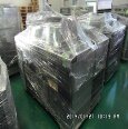
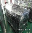
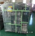
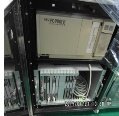
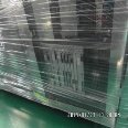
Used TEL / TOKYO ELECTRON Mark V #9130725 for sale
URL successfully copied!
Tap to zoom
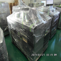


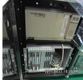

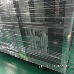

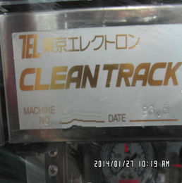

ID: 9130725
Wafer Size: 6"
Vintage: 1993
System, 6"
Left to Right
INDEXER 4 Cassette Stage (Uni-Cassette)
CONFIGURATION Main Body1 / Main Body2 / Chemical Cabinet
MAIN CONTROLLER NEC FC-9801X
C/S ROBOT TYPE Vacuum Arm / Ceramic Pincette
MAIN ROBOT TYPE 2 Pincette Arm
INDEXER Laser Diode Mapping Sensor
SCR JET Nozzle / Rinse Nozzle
COAT 4 Resist Nozzle / Bellows Pump
1 Gallon Resist Bottle / Thinner Local Supply (Canister)
EBR Nozzle / Back Rinse Nozzle
Local Drain (1ST SUS 10L Tank / Drain Pump)
DEV Nozzle Tyoe : Spray Nozzle
Rinse Nozzle / Back Rinse Nozzle
Facility Supply / Drain
WEE TEL Standard
CTV-410
AD TEL Standard
Local Supply (Canister)
1993 vintage.
TEL / TOKYO ELECTRON Mark V is a highly advanced photoresist equipment created by TEL (TOKYO ELECTRON Limited) for use in the semiconductor industry. The photoresist system incorporates proprietary technology and is comprised of several core components to make up TEL Mark V unit. The core component of TOKYO ELECTRON MARK-V machine is the photoresist unit, or PRU. It is a state-of-the-art, high-precision tool that utilizes sophisticated optical patterns to accurately apply the photoresist material to the semiconductor substrate. The photoresist unit uses a patented technology that is capable of accurately adjusting its pitch, size, and shape as well as applying a variety of sophisticated coatings. The unit is also able to work in a variety of temperature, pressure, and environment conditions to maintain a uniform and stable coating. This ability allows for high-quality results for all types of photoresist materials. MARK-V asset also features a number of other components, such as a precision high-speed robot for transferring masks and wafers, a high-speed film feeder for handling substrates, and a post-split model for aligning and cutting substrates into individual pieces. The equipment also includes a laser scanner for accurately reading barcodes and pattern marks, as well as an optical inspection system used to ensure the accuracy of film registration and masking. These components enable Mark V unit to provide high accuracy, repeatability, and precision required for the professional production of semiconductor products. In addition, the machine allows for an improved yield with minimal contamination and uniform coating quality across many different substrate sizes. TEL / TOKYO ELECTRON photoresist tool is also able to provide better environmental performance, by reducing the amount of hazardous chemical waste generated during the production process. TEL / TOKYO ELECTRON MARK-V asset also reduces power consumption thanks to its high-efficiency optical model, resulting in better energy efficiency. In addition, the equipment helps to reduce the total cost of semiconductor production by improving substrate throughput, minimizing rejects, and reducing defect-related damage costs. As one of the most advanced photoresist systems available today, TOKYO ELECTRON Mark V photoresist system is an ideal solution for semiconductor professionals looking to produce high-quality and consistent photoresist results. Its combination of sophisticated, precision components and efficient solutions makes it an excellent investment for those seeking to optimize their semiconductor production.
There are no reviews yet
