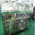
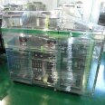
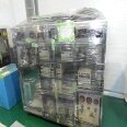
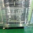
Used TEL / TOKYO ELECTRON Mark V #9130774 for sale
URL successfully copied!
Tap to zoom
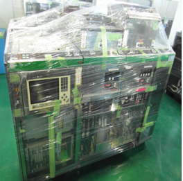

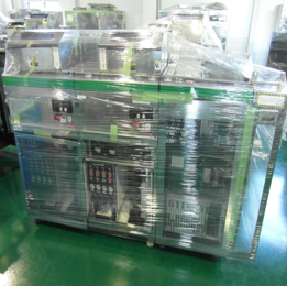


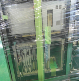

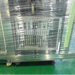


ID: 9130774
Wafer Size: 6"
Vintage: 1990
System, 6"
Left to Right
INDEXER 4 Cassette Stage (Uni-Cassette)
CONFIGURATION Main Body1 / Main Body2 / Chemical Cabinet
MAIN CONTROLLER NEC FC-9801X
C/S ROBOT TYPE Vacuum Arm / Ceramic Pincette
MAIN ROBOT TYPE 2 Pincette Arm
INDEXER Laser Diode Mapping Sensor
SCR JET Nozzle / Rinse Nozzle
COAT 4 Resist Nozzle / Bellows Pump
1 Gallon Resist Bottle / Thinner Local Supply (Canister)
EBR Nozzle / Back Rinse Nozzle
Local Drain (1ST SUS 10L Tank / Drain Pump)
DEV Nozzle Tyoe : Spray Nozzle
Rinse Nozzle / Back Rinse Nozzle
Facility Supply / Drain
WEE TEL Standard
CTV-410
AD TEL Standard
Local Supply (Canister)
1990 vintage.
TEL / TOKYO ELECTRON Mark V Photoresist equipment is an advanced photolithography solution designed to provide precise microstructures over large areas in a quick and efficient manner. The system combines laser beam direct lithography (LBDL) and conventional photolithography techniques, along with advanced patterning technology for successful pattern formation at the nanometer level. TEL Mark V unit is capable of creating three-dimensional structures that are difficult to develop by conventional photolithography processes. TOKYO ELECTRON MARK-V machine utilizes the KRS-U1100DL, a laser-generating device which has a maximum writing speed of 5m/s and a maximum repeat accuracy of 3nm. This device supplies a laser beam to a pattern formation device, which in turn, stores the pattern information in its internal memory and replays the pattern information onto the substrate. The laser beam applied onto the substrate is focused by a microscope tool into various microstructures. In addition, a built-in library enables the development of various micropatterns and structures including photoresist, overlay colored patterns and arrays, wafer circumference identification and via in/out contact. Using KRS-U1100DL, TOKYO ELECTRON Mark V asset has a minimum field feature size of 50nm and operates by applying a high frequency, short exposure time laser onto a resist-coated substrate. This laser has the ability to etch material at a much deeper level than other photolithography systems, enabling the development of three-dimensional structures far beyond the capabilities of conventional lithography machines. The model also features an advanced resist processing equipment which allows the formation of an extremely uniform and thin resist film across the entire substrate. This ensures accurate and repeatable pattern formation and provides a high-quality finish to every microstructure. Overall, TEL MARK-V Photoresist developed by TEL is a reliable and comprehensive photolithography solution. It features innovative pattern forming technology that enables the successful production of three-dimensional structures at the nanometer level and an integrated resist processing system for high-quality results. This unit is ideal for those who require precision pattern formation on their substrates for a wide range of applications.
There are no reviews yet
