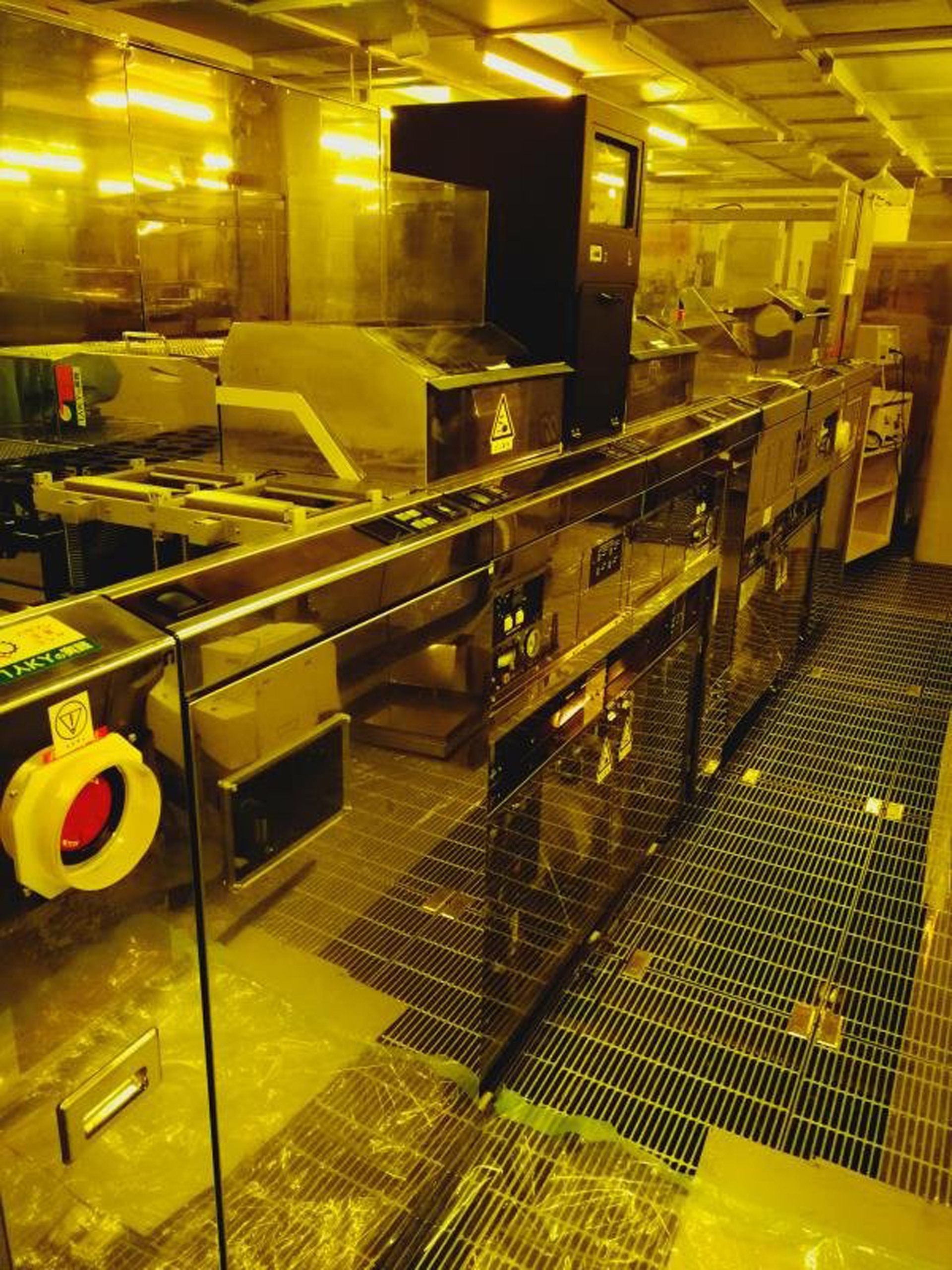
Used TEL / TOKYO ELECTRON Mark V #9222912 for sale
It looks like this item has already been sold. Check similar products below or contact us and our experienced team will find it for you.
Tap to zoom


Sold
ID: 9222912
Vintage: 1999
Systems
Utility:
Drive pressure:
Unit drive pressure: 3.5 kgf / cm² (343.2 kpa)
Ejector drive pressure: 3.5 kgf / cm² (343.2 kpa)
Resist pump drive pressure: 3.5 kgf / cm² (343.2 kpa)
Vacuum pressure:
Spinner: -550 mm Hg (-73.3 kpa)
WEE: -400 mm Hg (-53.3 kpa)
C/S, I/F(V,Vz): -400 mm Hg (-53.3 kpa)
N2 Pressure:
N2 Primary pressure: 3.5 kgf / cm² (343.2 kpa)
Developer solution canister tank pressure: 1.0 kgf/ cm² (98 kpa)
HMDS Supply tank pressure: 0.5 kgf / cm² (49 kpa)
Thinner supply tank pressure: 0.5 kgf / cm² (49 kpa)
Resist bottle pressure: 0.3 kgf / cm² (29.4 kpa)
Adhesion unit bubbler tank pressure: 0.3 kgf / cm² (29.4 kpa)
E2 Nozzle blow pressure: 0.3 kgf / cm² (29.4 kpa)
DI Water and developer solution:
Primary pressure: 1.0 kgf / cm² (98 kpa)
Secondary pressure: 1.0 kgf / cm² (98 kpa)
Chilly water:
Primary pressure: 1.5 kgf / cm² (147.1 kpa)
Exhaust pressure:
Coater cup: 5 mm H2O (0.05 Pa)
Developer cup: 10 mm H2O (0.1 Pa)
Scrubber cup: 10 mm H2O (0.1 Pa)
WEE Lamp house: 11∼13 mm H2O (0.11∼0.13Pa)
Temperature: 20~27° C Variance to be less than 0.5° C
Humidity: 28~55% RH Variance to be less than 3% RH
Power supply: 100/200 V, 50/60 Hz, Single phase, ±10%
1999 vintage.
TEL / TOKYO ELECTRON Mark V is a photoresist equipment. It is a device used to etch patterns onto a substrate (usually silicon wafers), and is used in semiconductor fabrication. It works by exposing a light sensitive film (photoresist) to light. The exposed areas are then developed and chemically processed. The result is a pattern etched onto the substrate. TEL Mark V is built with precision in mind. It has an advanced four-axis translation stage, allowing for precise position control over the substrate. It has a high resolution optical system with 4X to 10X adjustable magnification, allowing for accurate pattern resolution and alignment. The optical unit can be equipped with various illumination sources, including highly energy-efficient LED sources, as well as NIR and ultraviolet light sources. It is also equipped with an 'Auto Scan' feature to reduce exposure time and eliminate the potential for patterning errors due to misalignment. TOKYO ELECTRON MARK-V is an easy to use, reliable machine. It has an intuitive user-interface, and a range of features that make it easy to use for both novice and experienced users. It can be loaded with a range of photoresist materials, allowing for a wide range of patterning possibilities. It also features a 'Smart Nearest Neighbor' option, allowing for multiple exposures of the same photoresist layer, with each exposure optimized for the particular substrate. This feature improves pattern resolution and increases yield. MARK-V also has a built-in touch-panel monitor to provide users with information about the operation of the tool. This includes information about the process parameters, as well as warnings and alarms. This ensures that users can monitor the process in real time, and adjust parameters accordingly. TOKYO ELECTRON Mark V is an advanced, easy to use photoresist asset that provides accurate patterning at a high throughput. It is ideal for use in semiconductor fabrication, and is reliable and user-friendly enough to be used by both experienced and novice users.
There are no reviews yet