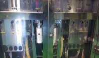
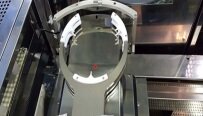
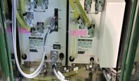
Used TEL / TOKYO ELECTRON Mark V #9234099 for sale
URL successfully copied!
Tap to zoom
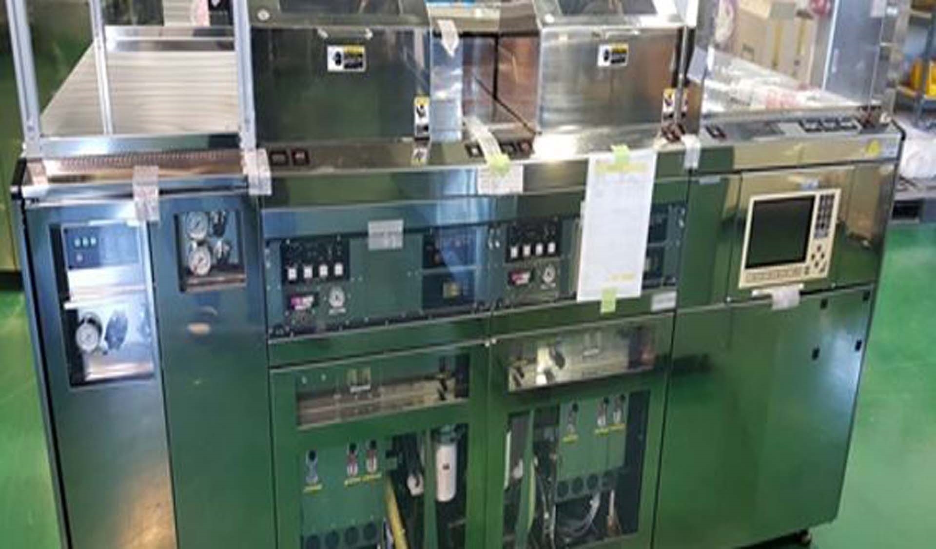

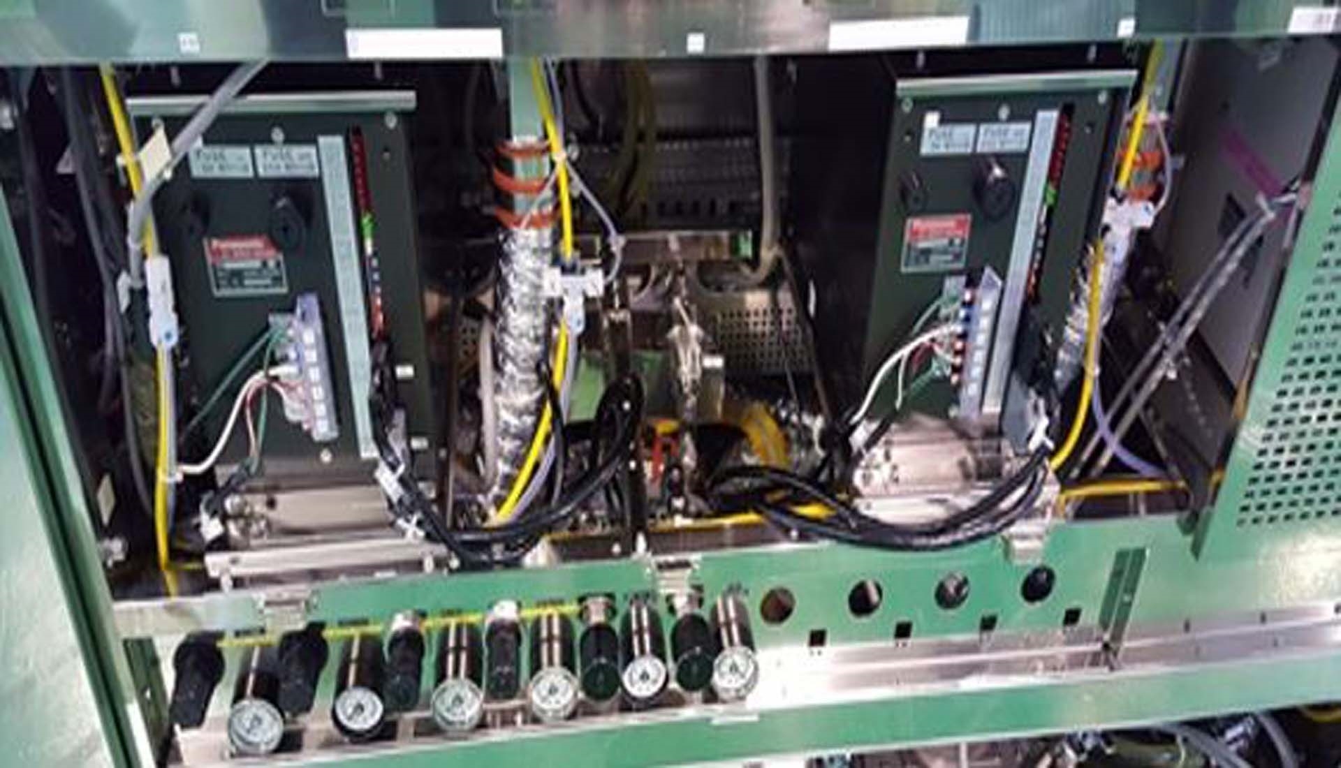

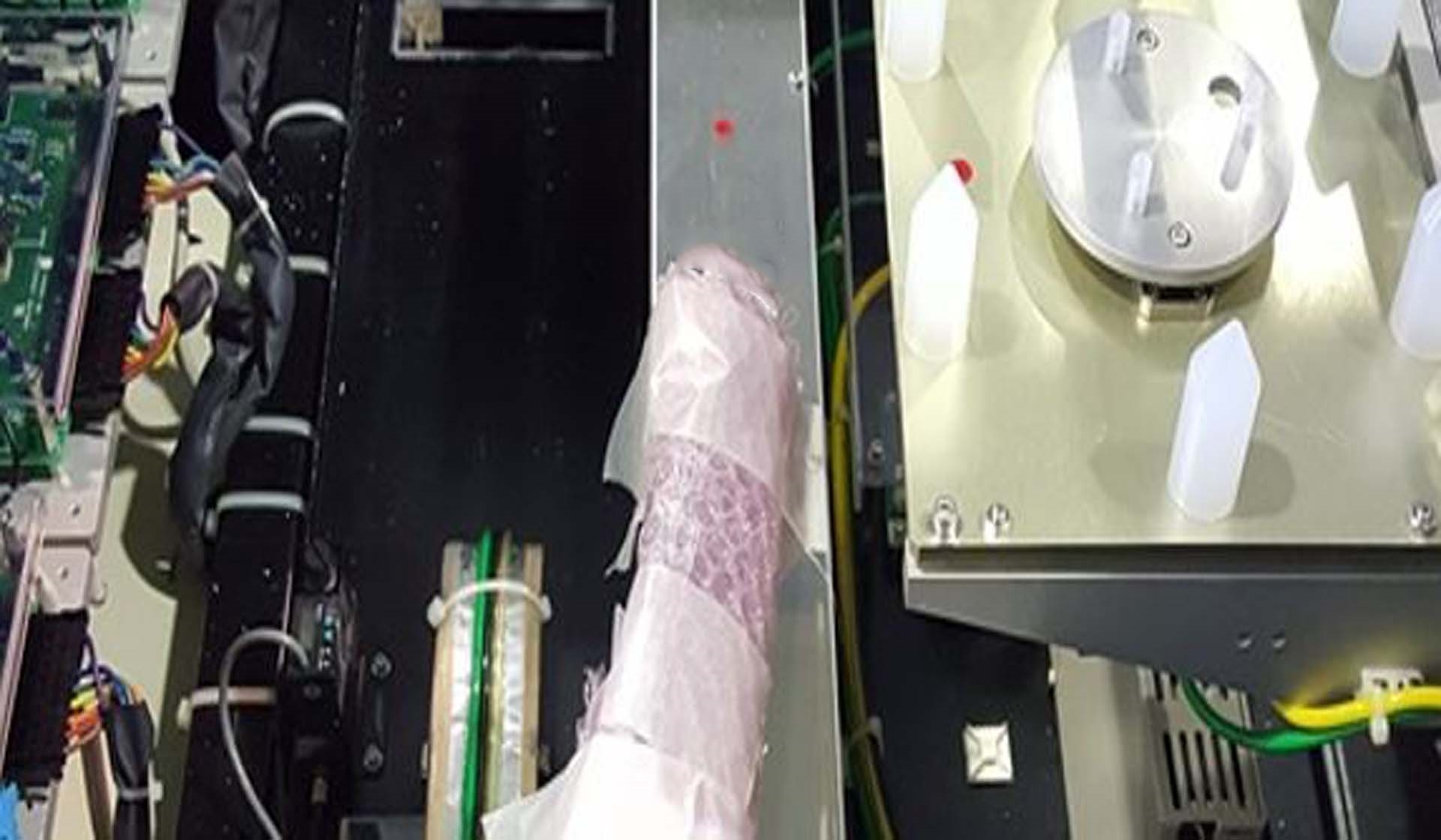


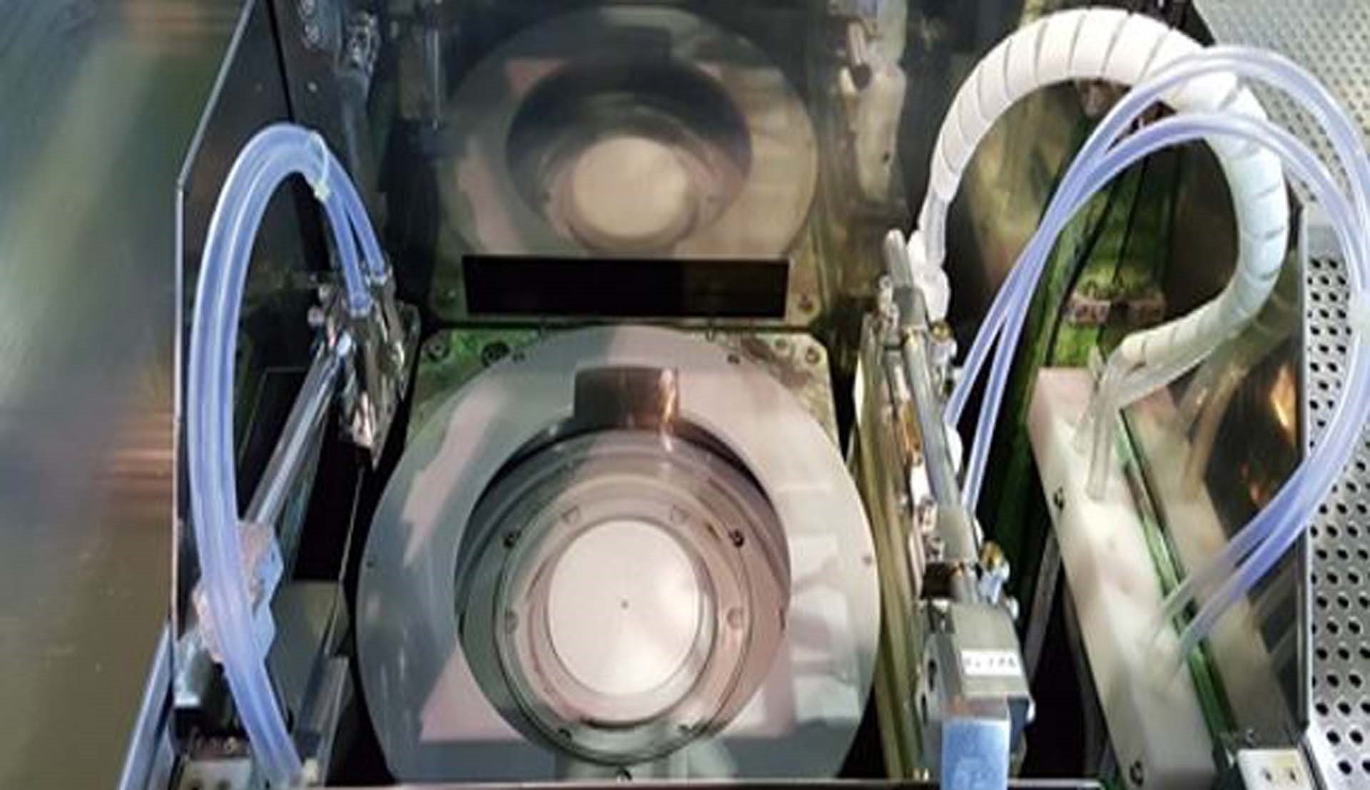


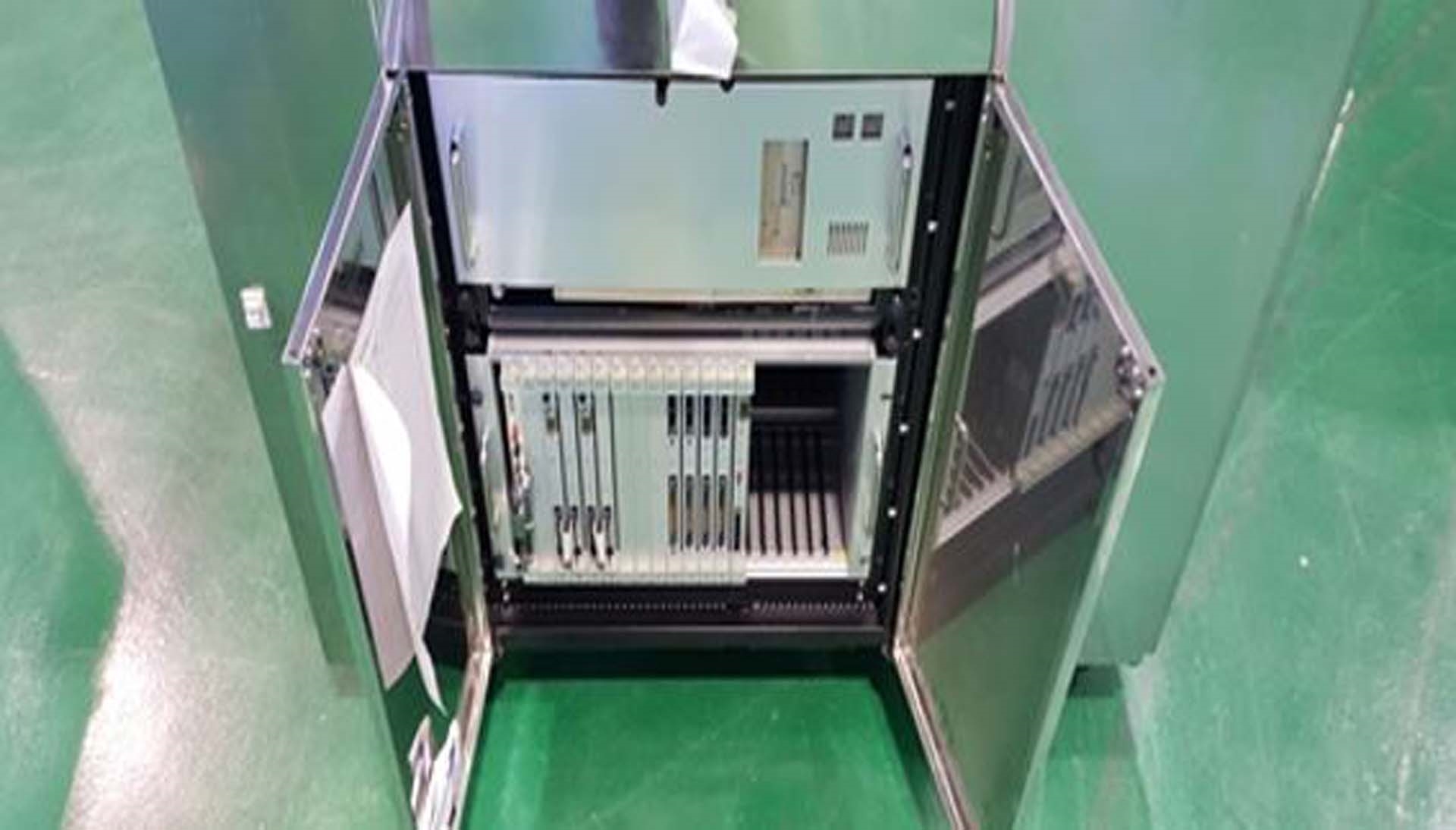


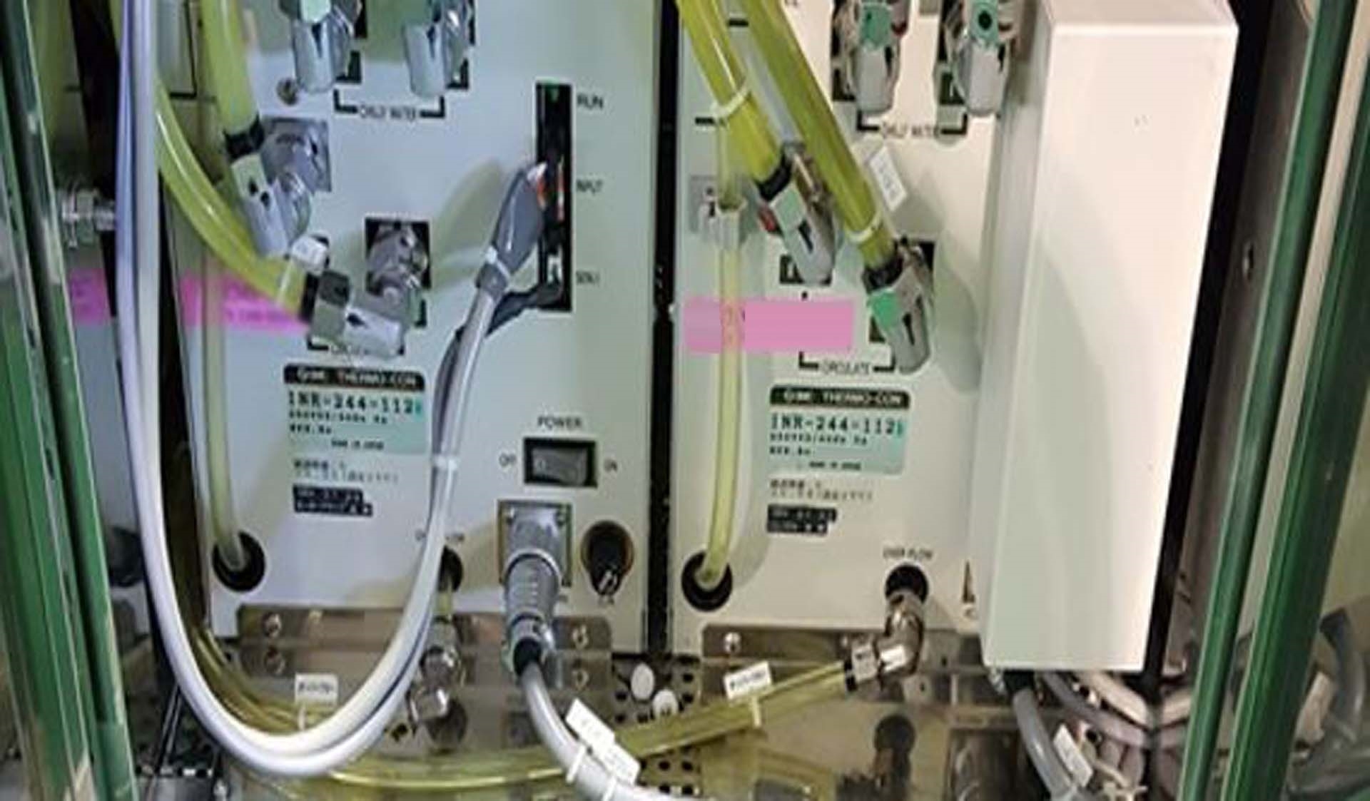


ID: 9234099
Wafer Size: 6"
Vintage: 1993
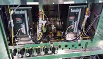
Track system, 6"
Direction flow: Left to right
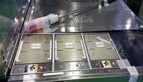
Indexer:
(3) Cassette stages (Uni-cassette)
Laser diode mapping sensor
Configuration: Main body
Main controller: FC-9801X
C/S Robot type: Steel blade
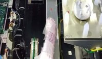
Main robot type: (2) Pincette arms
Chemical purge
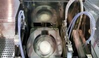
Developer:
Nozzle type: E2 Nozzle
Rinse nozzle
Facility drain
No Chemical cabinet
No THC
Missing parts:
Temperature controller
Monitor
1993 vintage.
TEL / TOKYO ELECTRON Mark V is a photoresist equipment developed by TEL Ltd. This system is designed to offer improved lithography processes to semiconductor manufacturers. It utilizes a stepper and scanner combination axis, which helps to accurately and reliably transfer a circuit pattern onto a large area substrate. TEL Mark V is equipped with an integrated digital signal processing (DSP) environment, which simplifies the control of processes, reduces the need for manual intervention and simplifies recipe development. It also has a LEAP Semiconductor Inspection Unit which provides high resolution imaging with multiple wavelengths of light for testing purposes. The LEAP machine can also measure in-die process characteristics and corrective actions can then be taken as necessary. Further, the tool includes a surface tension module and an ultrathin topcoat. This allows for the formation of a super-smooth surface, eliminating any disturbances that could be caused by surface variation. This ensures uniform deposition, and prevents the creation of subtle trenches and ridges which can cause distortion in the transfer process. In addition, it is equipped with a maskless lithography asset which features UV exposure with multiple laser covers. This allows for a faster and more precise exposure process, with a minimum of line width variations. It also has a high power laser which reduces line loss and increases overlay precision. Overall, TOKYO ELECTRON MARK-V model offers a reliable and sophisticated lithography process for advanced semiconductor manufacturing requirements. It is designed for ease of use, with an intuitive user interface, as well as, its high precision, and variable overlapping of various process parameters makes it one of the most versatile systems available.
There are no reviews yet

