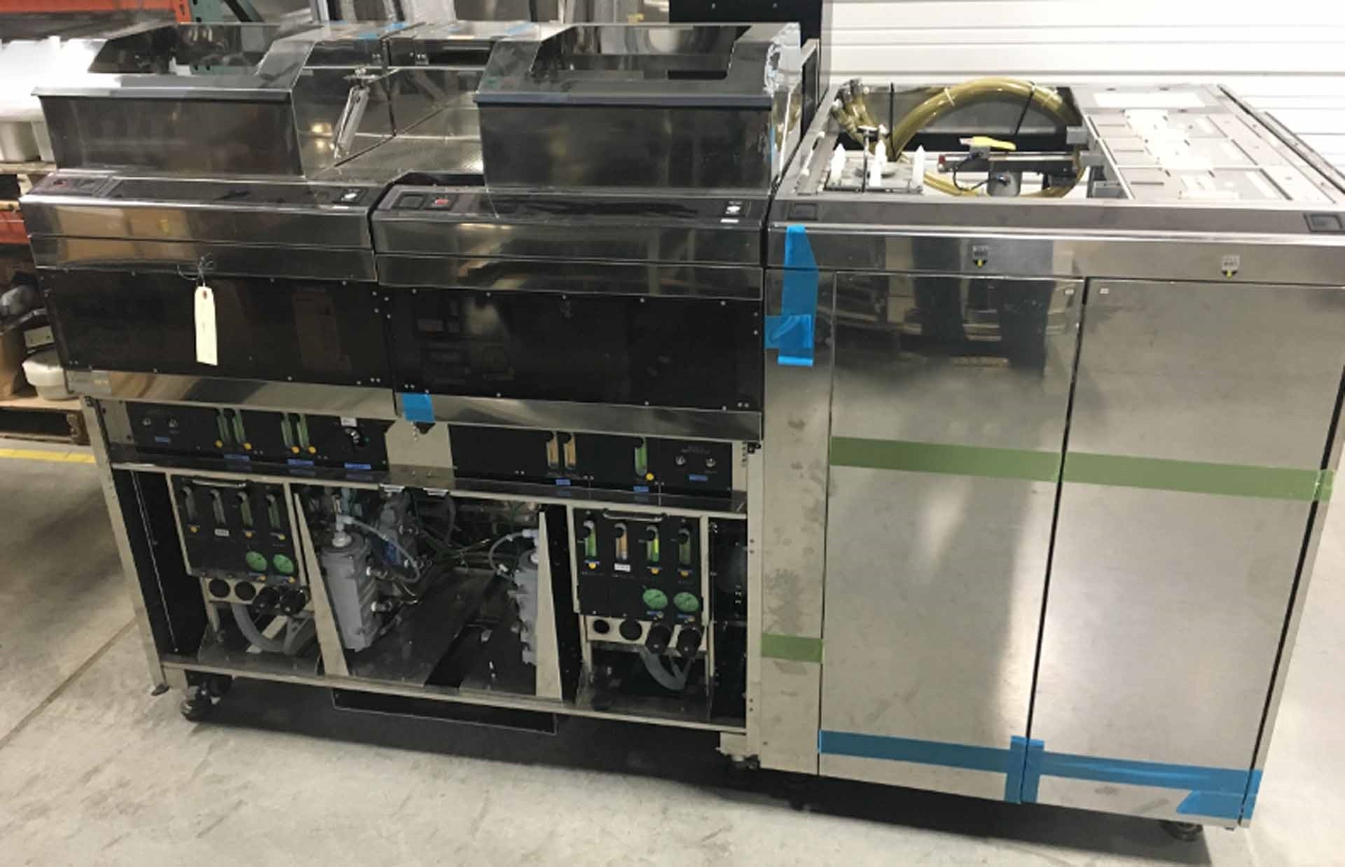
Used TEL / TOKYO ELECTRON Mark V #9241680 for sale
It looks like this item has already been sold. Check similar products below or contact us and our experienced team will find it for you.
Tap to zoom


Sold
ID: 9241680
Wafer Size: 6"
(2) Developer system, 6"
TC Rack / Chemical cabinet
WEE Configuration
(2) COL
4HP.
TEL / TOKYO ELECTRON Mark V (TEL/TEMV) is a photoresist equipment used for semiconductor device production processes. It is designed to be a multi-purpose, high-throughput tool for post-wafer fabrication of advanced semiconductor devices. TOKYO ELECTRON/TEMV system features a unique direct write, semi-automated operation that enables precise and repeatable processing effects. It is equipped with a high-accuracy laser-writing head, a powerful registration platform, and a high-efficiency mini-scan unit. These advancements ensure that TEL / TOKYO ELECTRON/TEMV produces superior and highly accurate photoresist patterns. The primary use of TEL/TEMV machine is for processing thin-film transistors (TFTs) that are used in flat panel displays. TFTs help control the voltage and current of displayed images and provide a sharp, high-definition image to the screen. Through using TOKYO ELECTRON/TEMV, the key steps required to deposit the metal film or fabricate oxide materials on the TFT devices are executed in high accuracy and high speed. TEL / TOKYO ELECTRON/TEMV tool is also applicable to some of the advanced integrated circuit (IC) processes. This includes the formation of trench structures and 3D transistors as well as the conducting layer patterning process. This enables higher circuit speeds, higher resolution, and better overall performance, all while still achieving excellent levels of precision and consistency in the photoresist patterning process. TEL/TEMV asset produces photoresist patterns that are compatible with a wide variety of materials and profiles. This includes polymers, conductive substrates, and single-wafer structures. Its wide range of materials compatibility and continuous operation enable better throughput, lower cost, and more consistent patterning. In addition, TOKYO ELECTRON/TEMV model is designed to be extremely user-friendly. It makes use of a range of automatic controls, which allow for quick and easy set up of a wide variety of sub-processes and materials. The equipment also has an intuitive user interface which enables easy control over the system and process parameters. TEL / TOKYO ELECTRON/TEMV is an excellent tool for semiconductor production processes, as it offers superior accuracy, throughput, and repeatability. Its advancedfeatures also provide for optimal performance, resulting in highly reliable and precise photoresist patterns for various semiconductor applications.
There are no reviews yet