Used TEL / TOKYO ELECTRON Mark V2 #293820865 for sale
URL successfully copied!
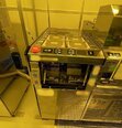

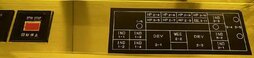
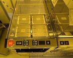
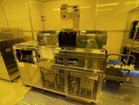

Tap to zoom
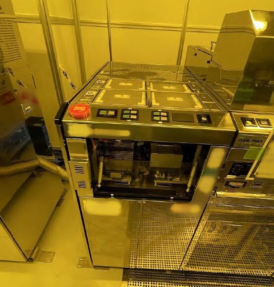

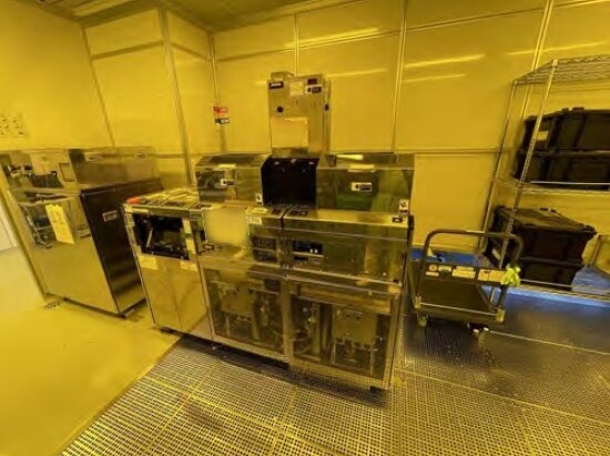
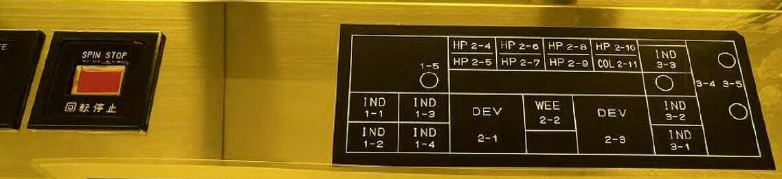
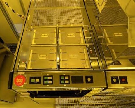
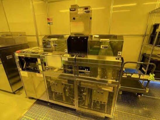

ID: 293820865
Wafer Size: 6"
Vintage: 1995
Positive photoresist developer, 6"
1995 vintage.
TEL / TOKYO ELECTRON Mark V2 is a state-of-the-art photoresist equipment designed for advanced semiconductor lithography processes. This system plays a critical role in patterning integrated circuits by transferring circuit patterns onto semiconductor wafers through a series of precise photolithography steps. By utilizing advanced technologies and innovative features, TEL Mark V2 offers unparalleled performance, precision, and reliability required for high-volume semiconductor manufacturing. One of the key features of TOKYO ELECTRON Mark V2 is its high-resolution capability, which allows for the fabrication of ultrafine patterns on semiconductor wafers. This unit leverages advanced optics, precision stages, and intelligent software algorithms to achieve sub-micron resolution, enabling the production of cutting-edge semiconductor devices with densely packed features and high levels of integration. In addition to high resolution, Mark V2 excels in process control and uniformity, ensuring consistent patterning across the entire surface of the wafer. This machine incorporates advanced monitoring and feedback mechanisms to optimize exposure dosage, focus, and alignment during the lithography process. By maintaining tight tolerances and controlling process variations, TEL / TOKYO ELECTRON Mark V2 enables the production of uniform and defect-free patterns, essential for the reliability and performance of semiconductor devices. TEL Mark V2 also offers outstanding process flexibility, supporting a wide range of photoresist materials and processing conditions to meet diverse application requirements. Whether for logic devices, memory components, or advanced packaging solutions, this tool can adapt to different process recipes and deposition techniques, providing manufacturers with the versatility needed to address various technology nodes and device architectures. Moreover, TOKYO ELECTRON Mark V2 incorporates advanced automation and connectivity features to streamline operations and enhance productivity in semiconductor fabrication facilities. With intuitive user interfaces, remote monitoring capabilities, and data analytics tools, operators can efficiently program, monitor, and analyze lithography processes, reducing cycle times and improving overall yield and throughput. Furthermore, Mark V2 emphasizes reliability and uptime, with robust design features and proactive maintenance strategies to minimize downtime and ensure continuous operation in high-volume manufacturing environments. This asset is engineered for long-term performance and durability, enabling semiconductor manufacturers to achieve high levels of process stability and consistency over extended production runs. Overall, TEL / TOKYO ELECTRON Mark V2 represents a cutting-edge solution for semiconductor lithography, offering exceptional resolution, process control, flexibility, and reliability to meet the demanding requirements of the semiconductor industry. With its advanced technologies and innovative capabilities, this model enables manufacturers to produce next-generation semiconductor devices with superior performance, efficiency, and reliability, driving innovation and advancement in the global semiconductor market.
There are no reviews yet