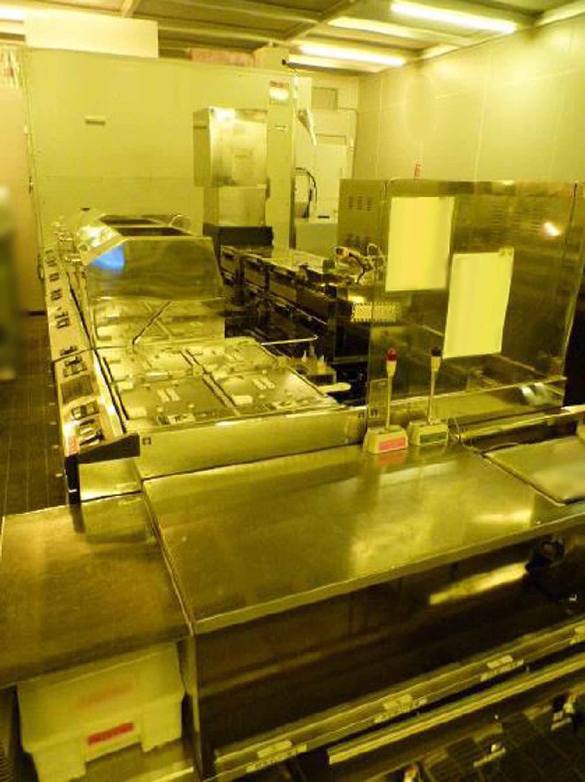
Used TEL / TOKYO ELECTRON MARK Vz #9221713 for sale
URL successfully copied!
Tap to zoom


ID: 9221713
Wafer Size: 6"
Vintage: 1994
(1) Coater / (2) Developer system, 6"
With scrubber
Missing parts:
TEL Vac solenoid valve
TEL Resist 1 cap
TEL Resist 2 cap
TEL Resist 3 cap
TEL Resist 4 cap
TEL Cup controller (Humidity)
TEL Timing belt, P/N: 023-101053-1
WATANABE Interferometer laserhead
SSM DEVE Spin motor
TEL WEE Shutter photo sensor
TEL DEVE Edge ring
TEL Circulator pump
TEL Resist pump4
TEL M/A θDriver
TEL M/A θBelt
TEL M/A Z Motor
TEL DEVE Drive
TEL Humidity sensor
1994 vintage.
TEL / TOKYO ELECTRON MARK Vz is a best-in-class, high-precision 'photoresist' equipment designed for photomask exposure and etching in semiconductor production. It is used for imaging and patterning of circuits for microelectronics and optics. The system is equipped with micro-optical and projection imaging systems for handling a range of substrates including metals, polymers, organics and ceramics. The machine can handle substrates as small as 0.05mm in size. The unit also incorporates high-resolution cameras to detect and adjust for substrate curvature, ensuring that each exposure is accurate and consistent. The machine features a uniform, high-speed UV laser scanner and a wide-field optical microscope for accurate alignment of the laser beam. This technology enables the machine to precisely control exposure dose and print quality. The tool also has a high-speed automatic wafer handling asset. The model is capable of aligning the substrate accurately in both the xaxis and y-axis to achieve best-in-class exposure uniformity. The equipment is equipped with a mask cleaning system to ensure no dust or other particles contaminate the mask or the substrate during the exposure process. This unit uses advanced algorithms to locate and identify any potential contaminants and remove them from the substrate. The machine also features a highly precise developing tool that is able to control the amount of developer used to ensure accuracy in the developing process. It also features an imaging library that can store up to 400,000 images of previously developed patterns. Finally, the asset is capable of providing metrology services that help to ensure that the exposed resist is at the desired thickness and the developed resist features consistent pattern quality. This helps to ensure that the devices produced through imaging are of the highest quality.
There are no reviews yet