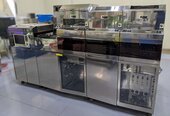
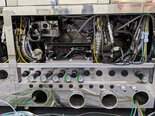
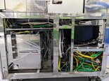
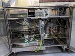
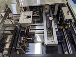
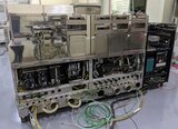
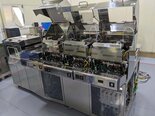
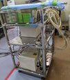
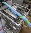
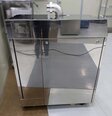
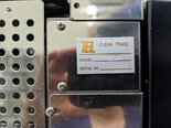
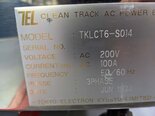
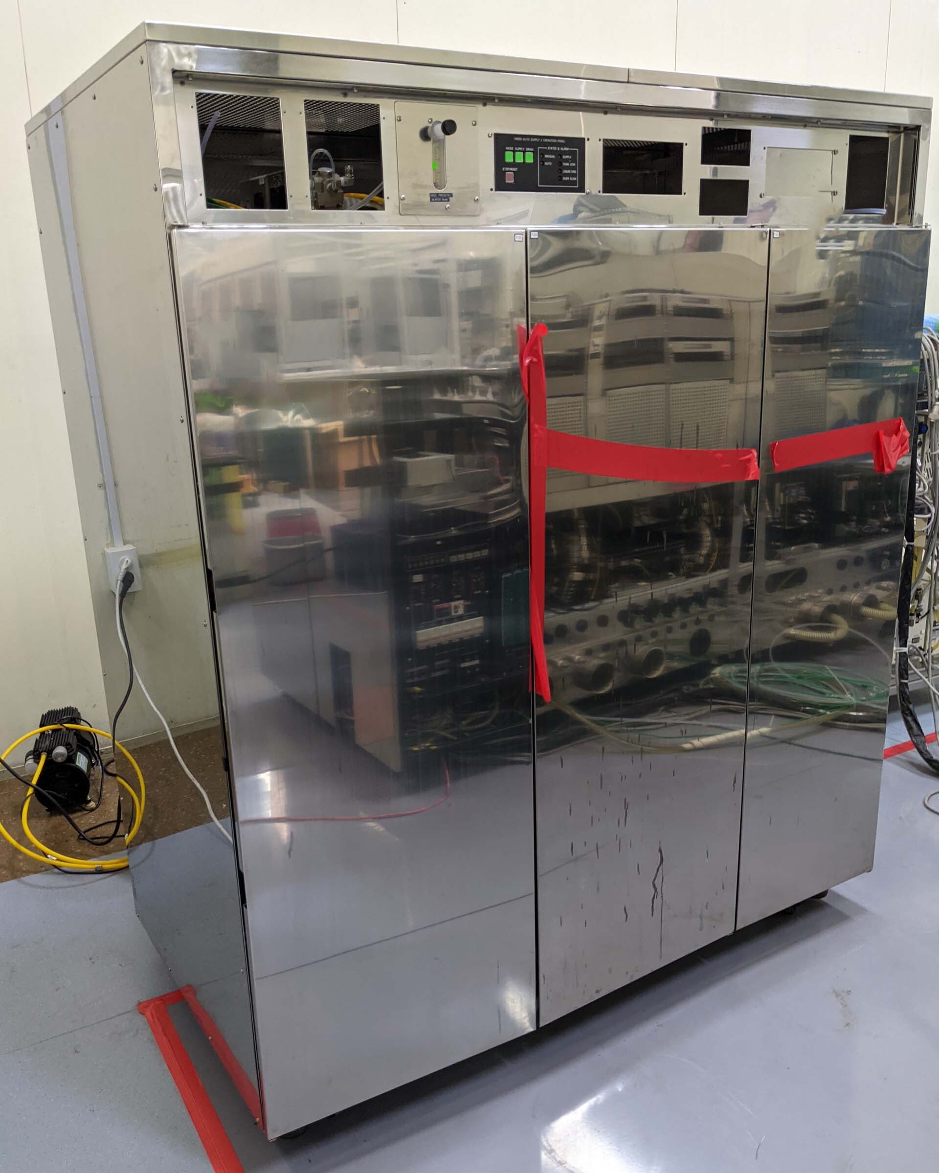
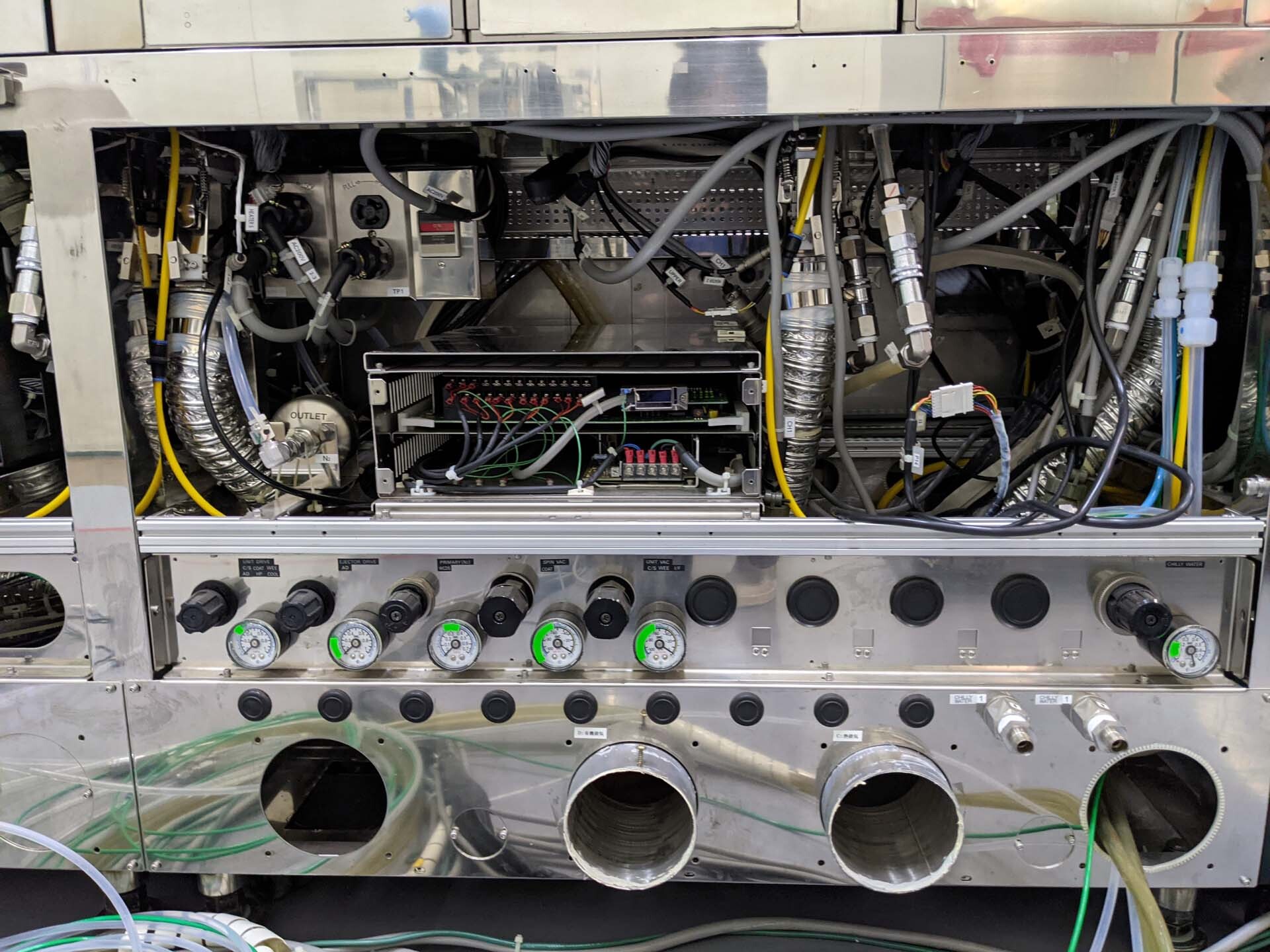
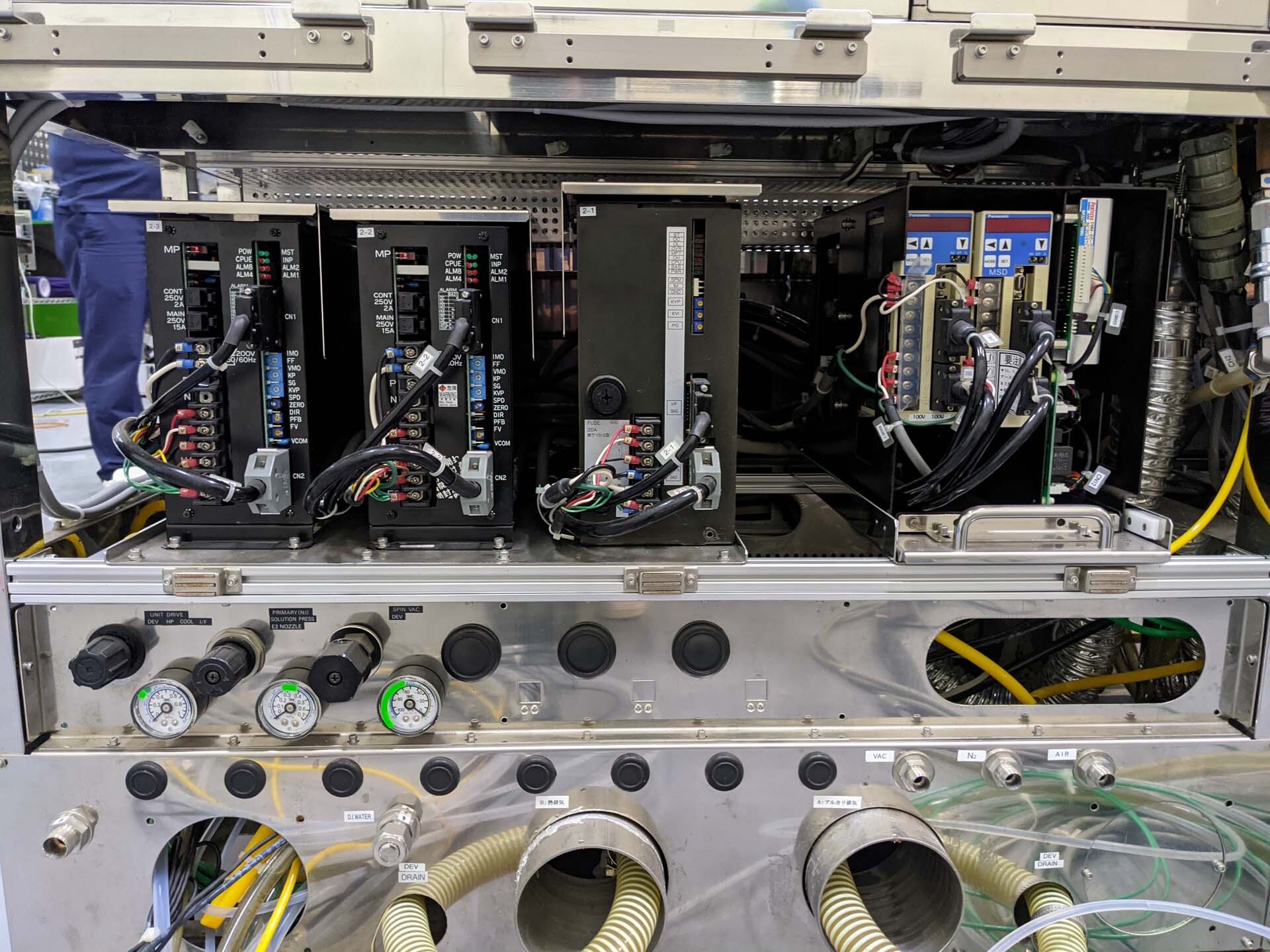
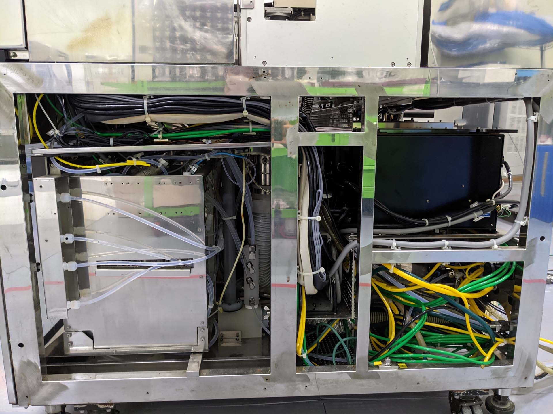
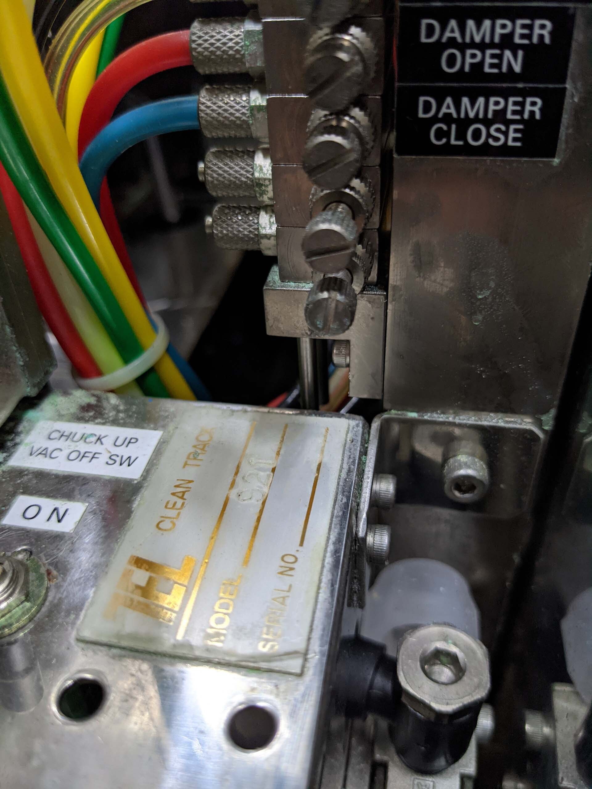
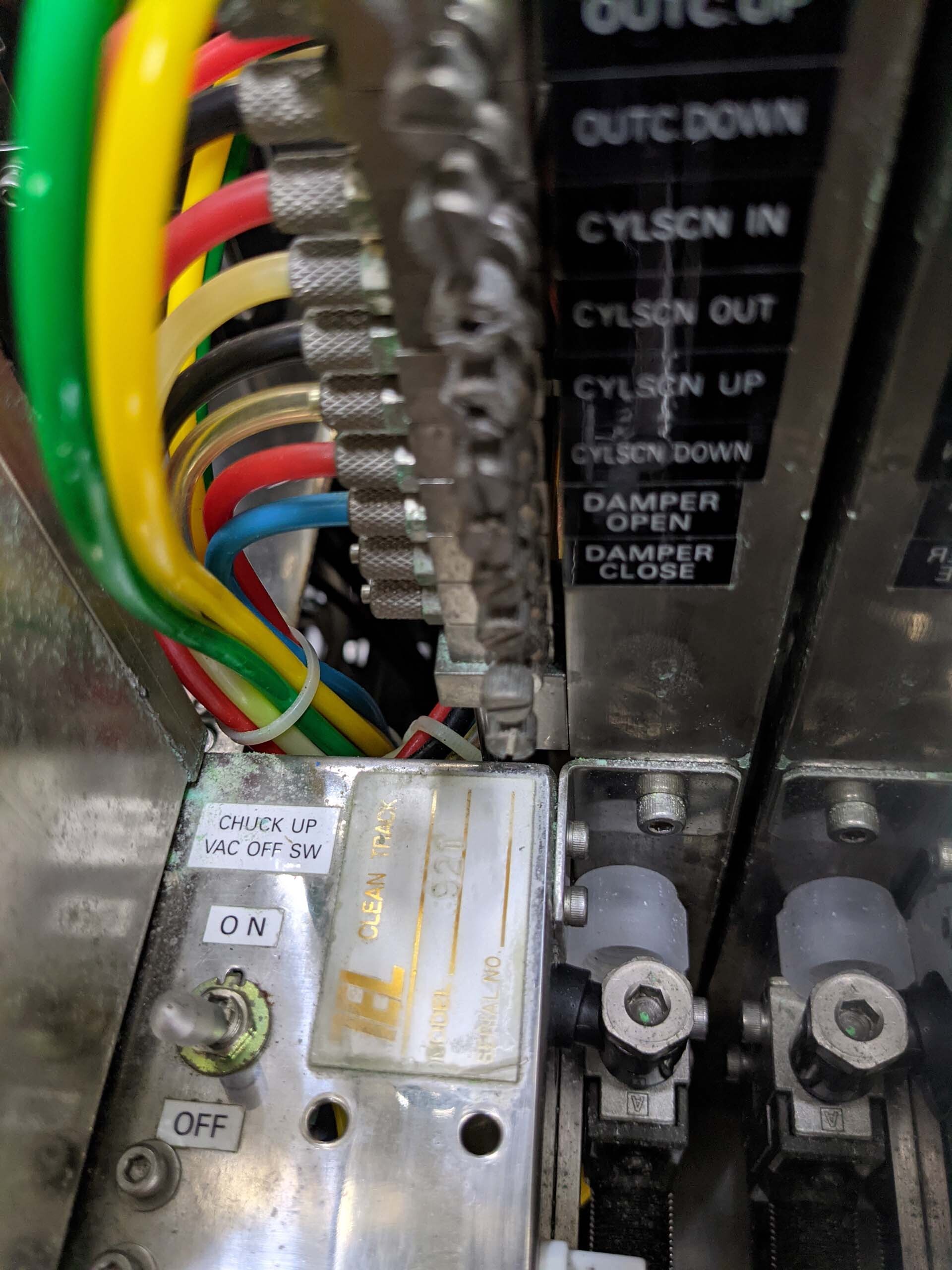
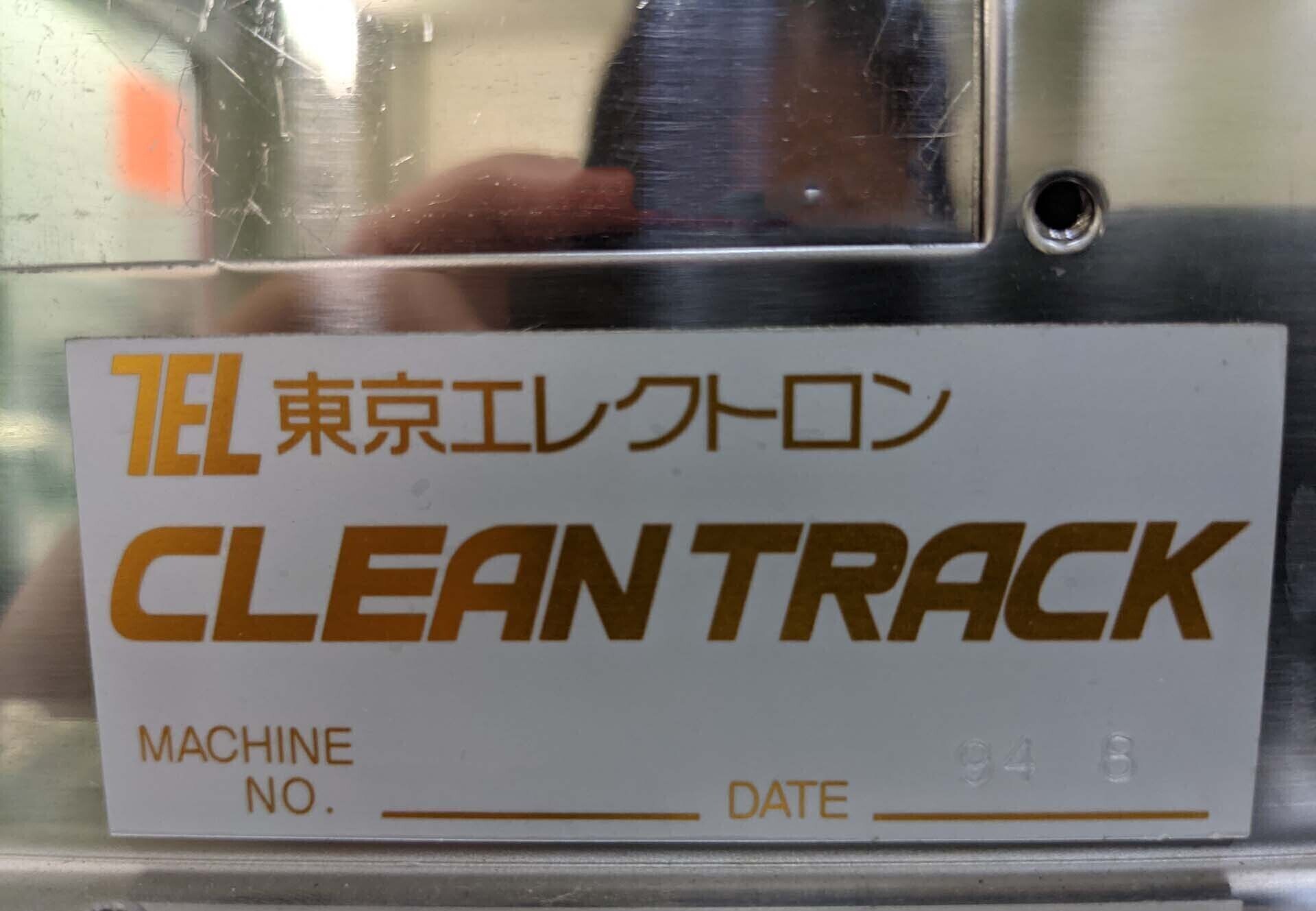
Used TEL / TOKYO ELECTRON MARK Vz #9386549 for sale
URL successfully copied!
Tap to zoom































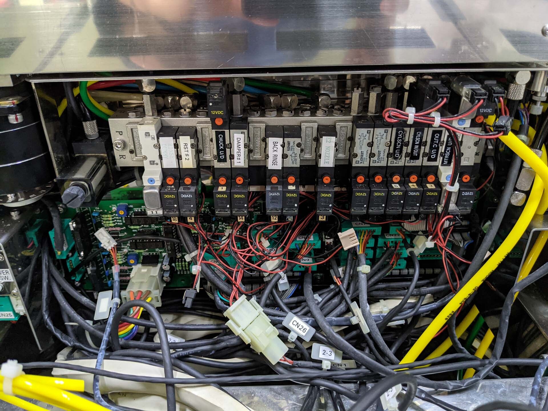

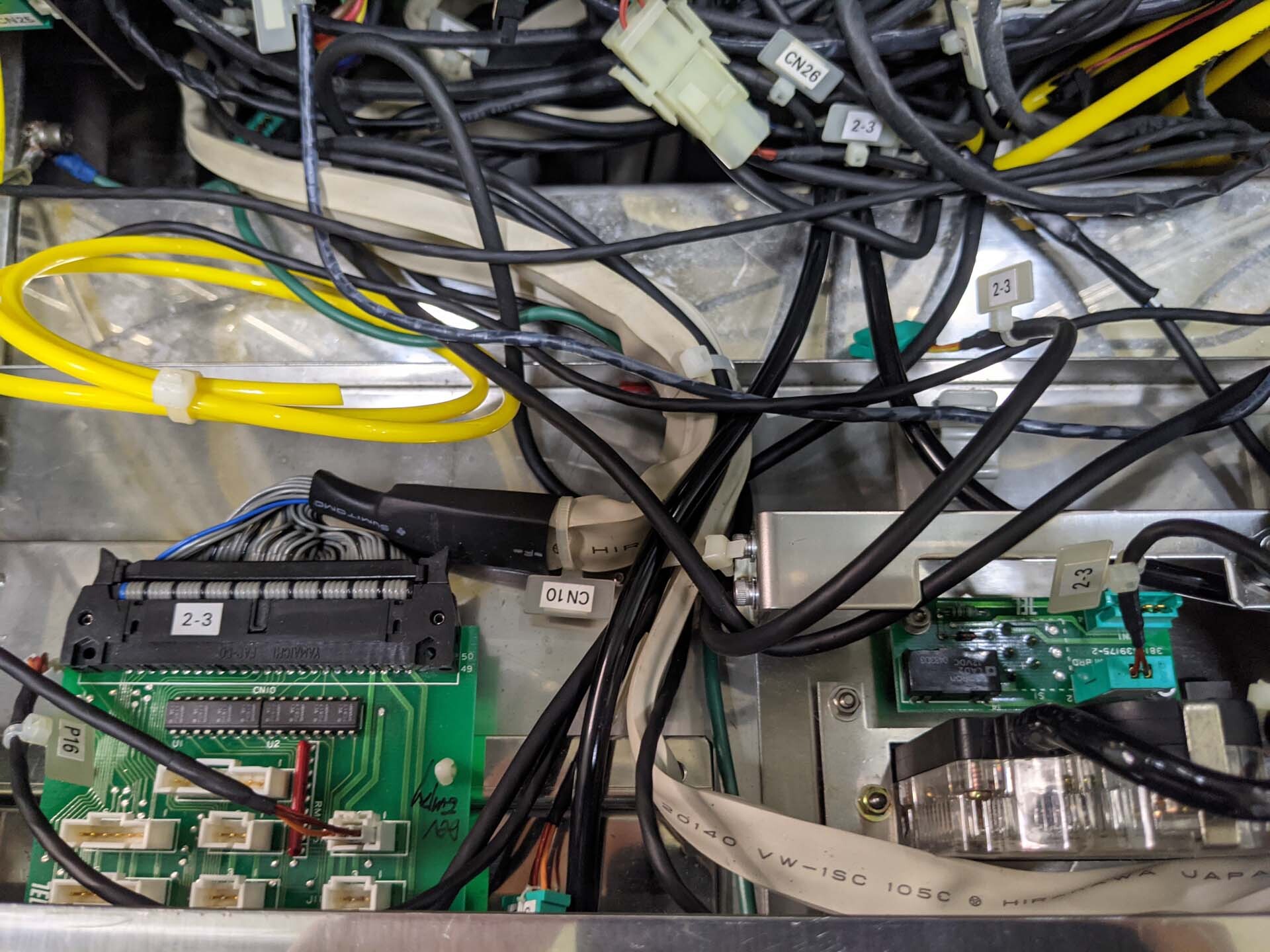


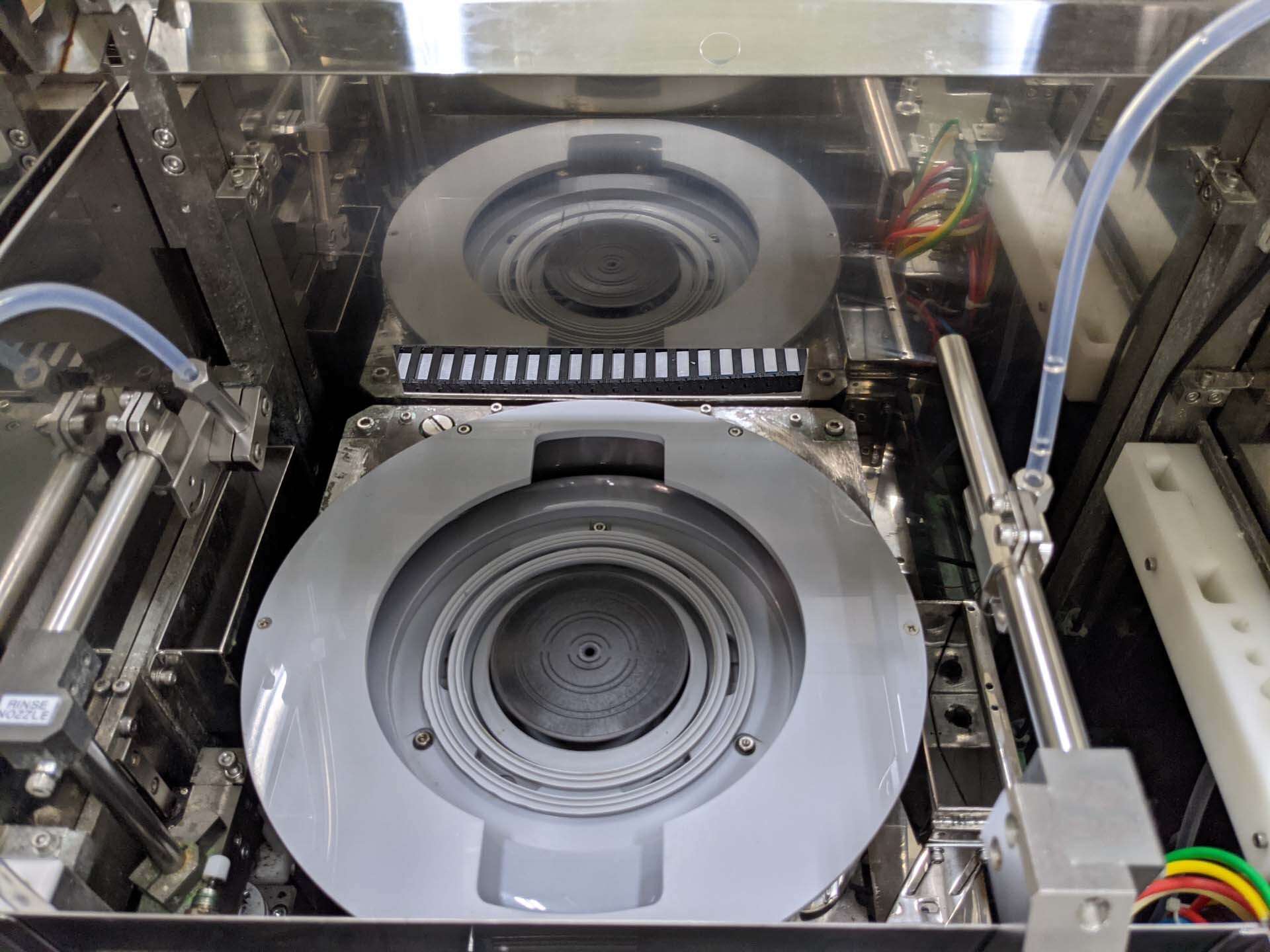

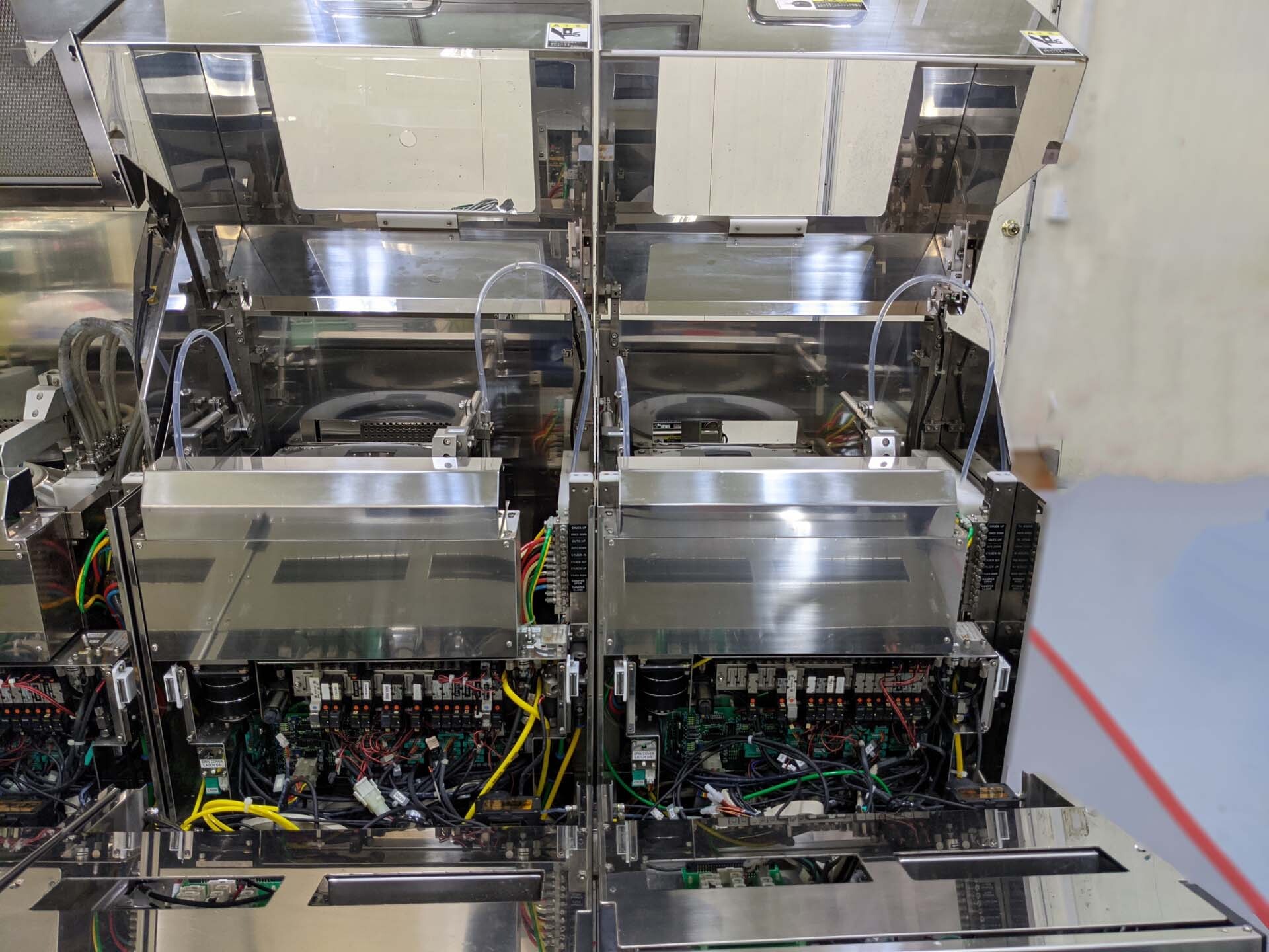

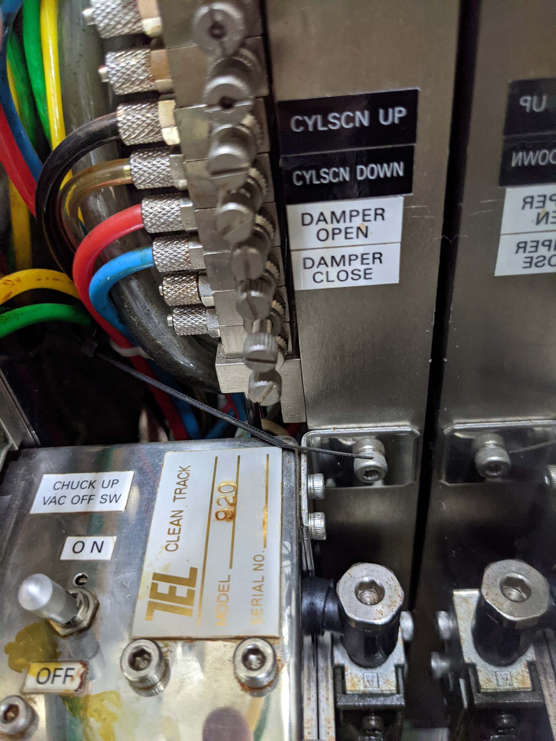

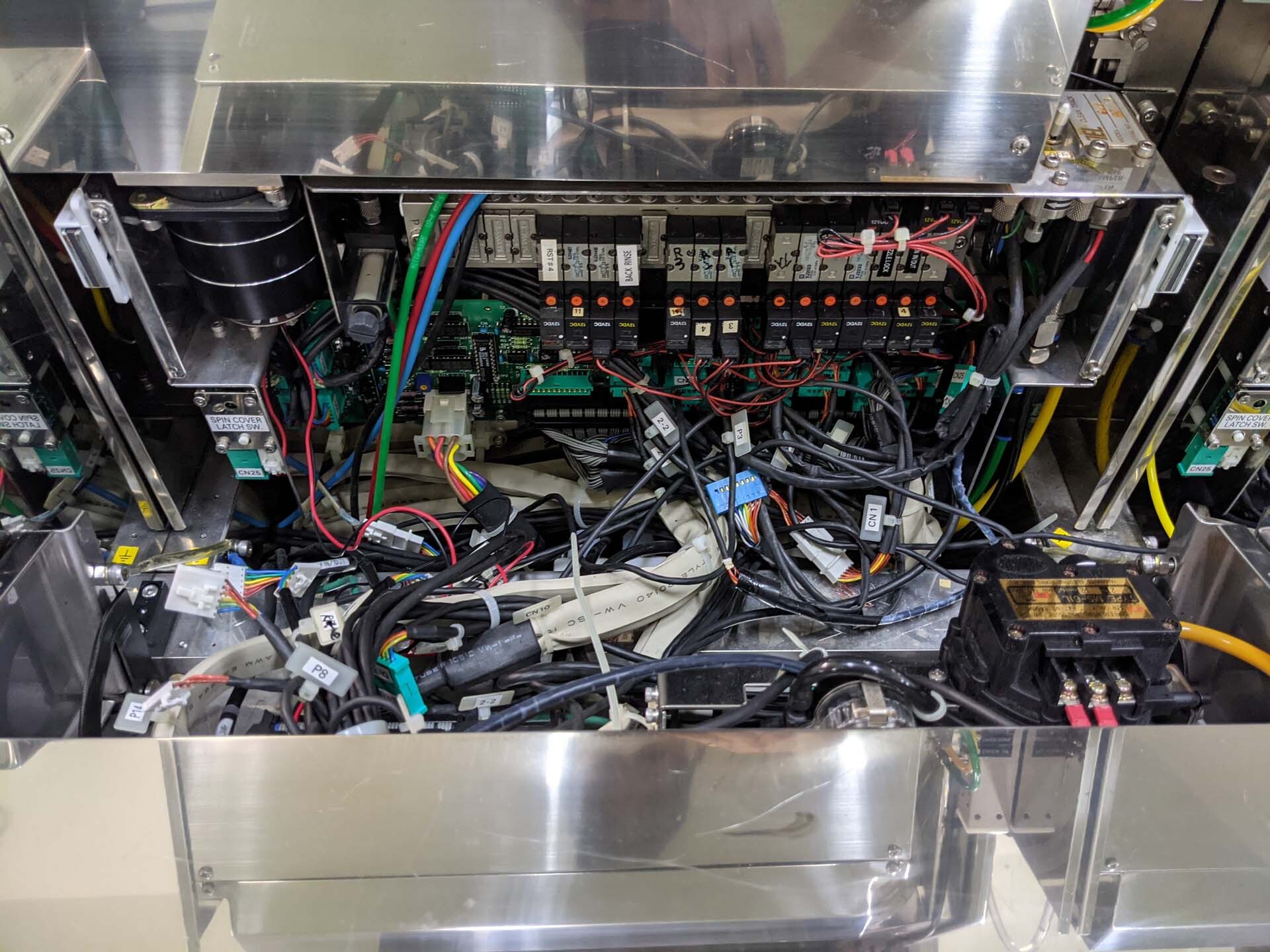

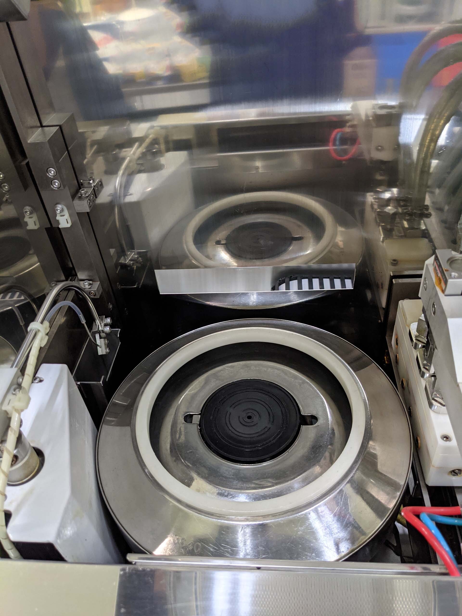


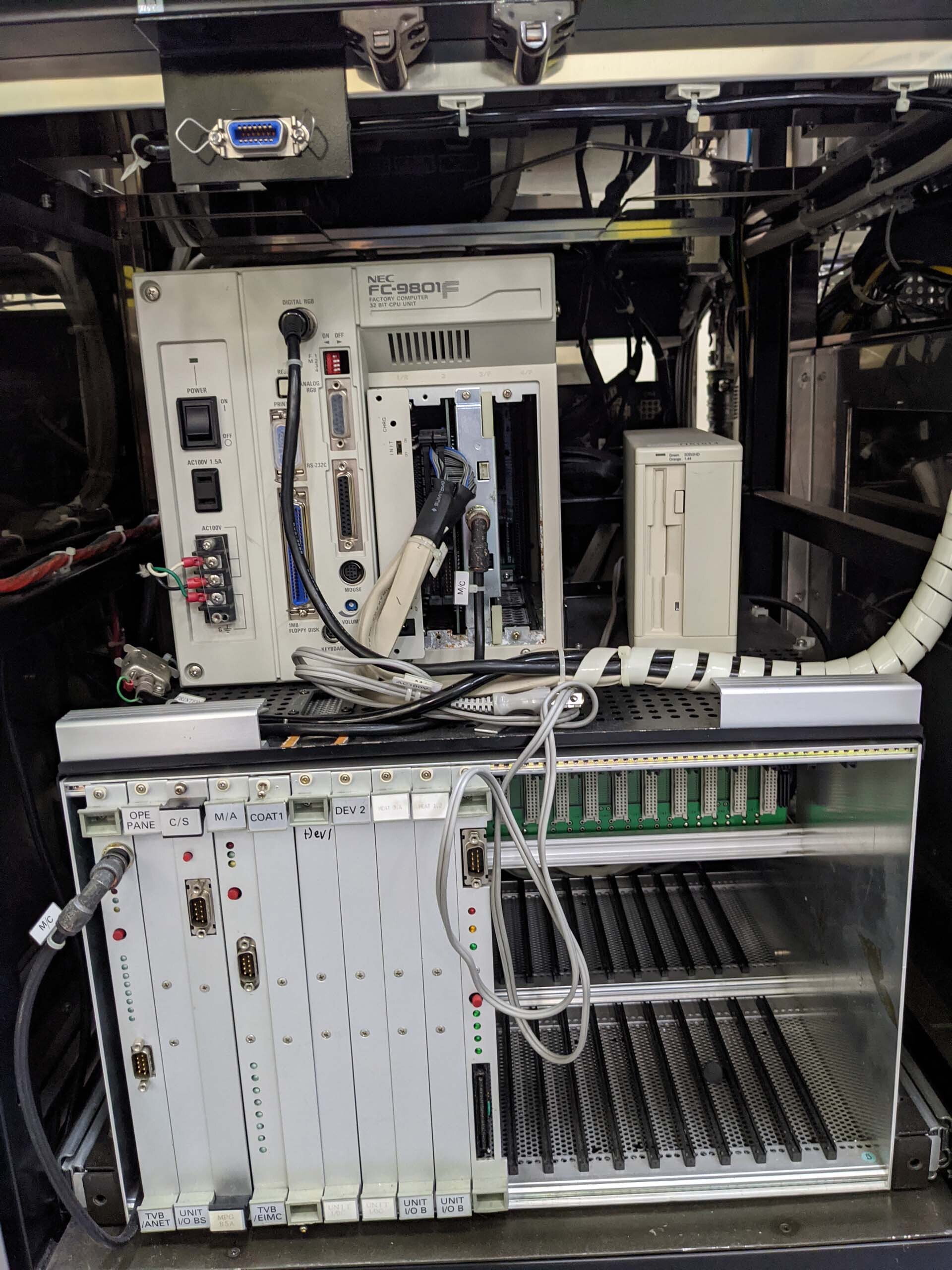







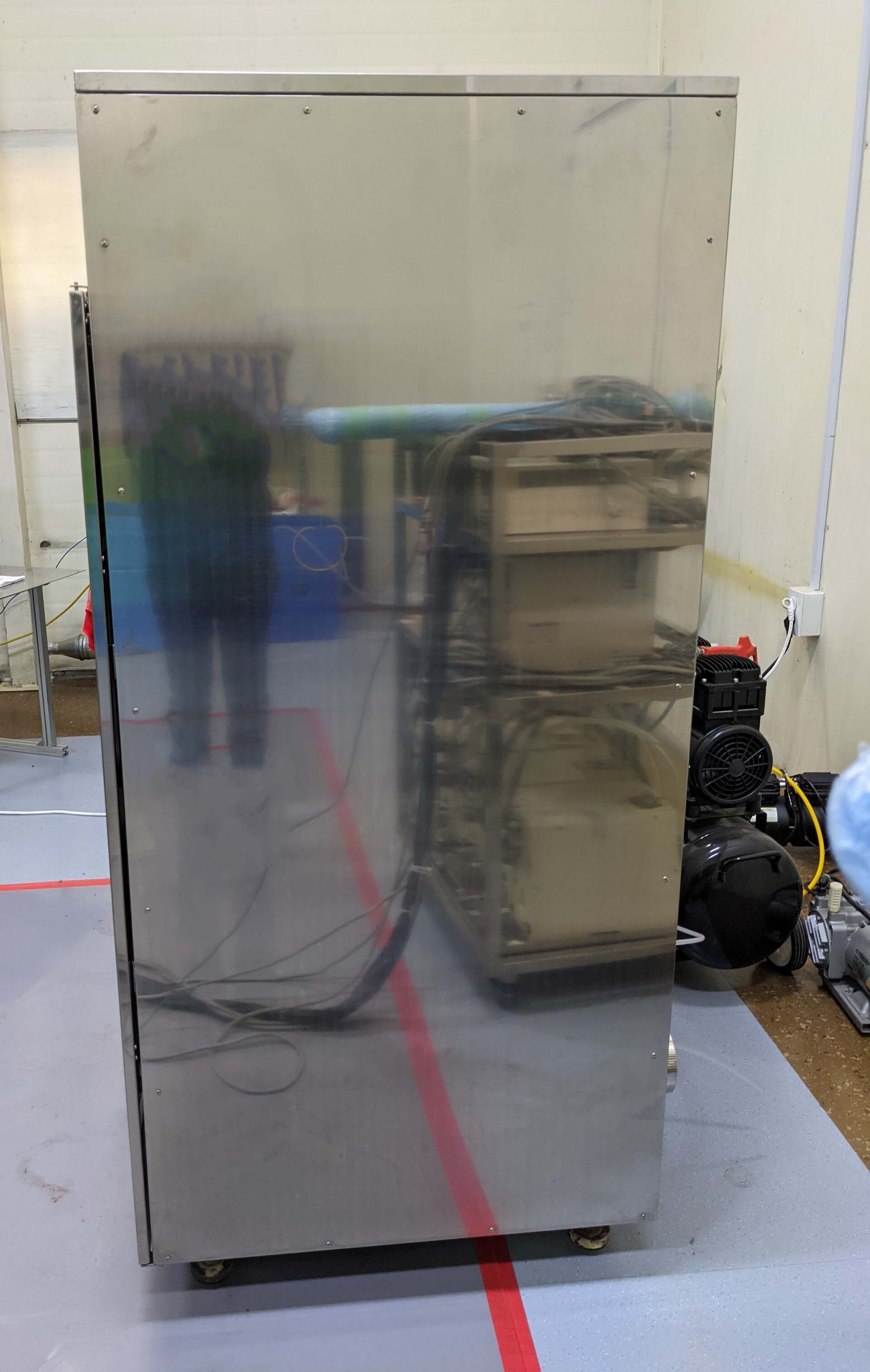


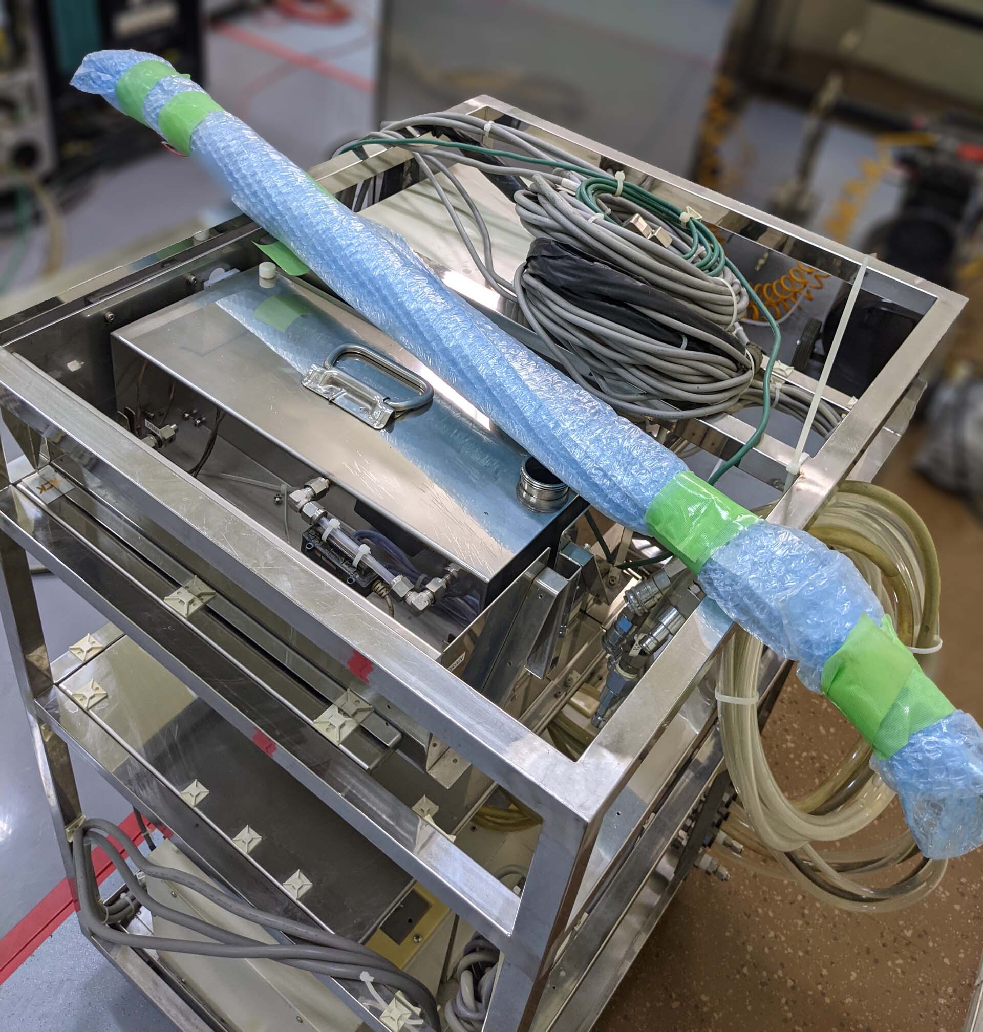


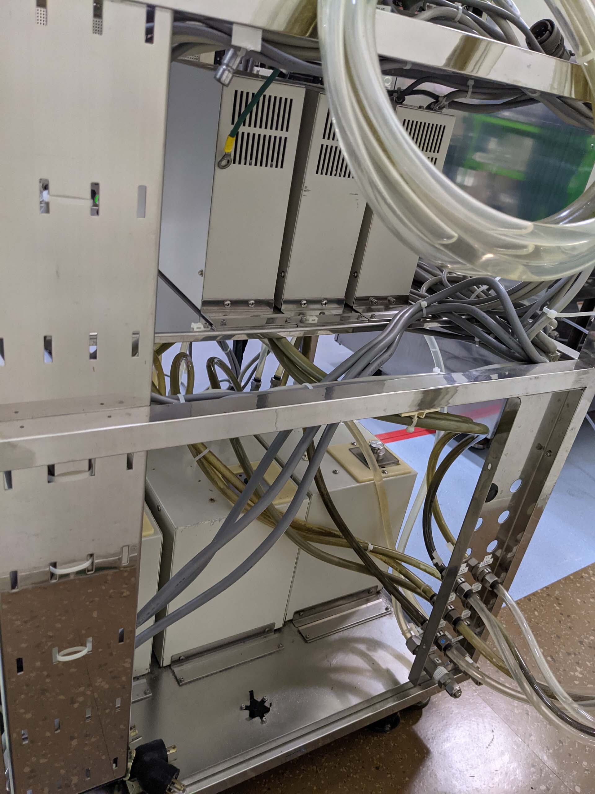

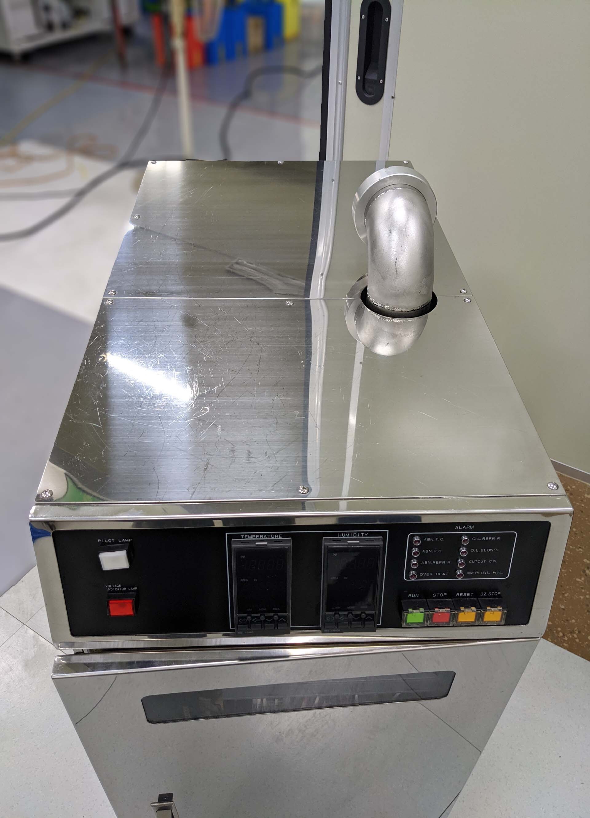


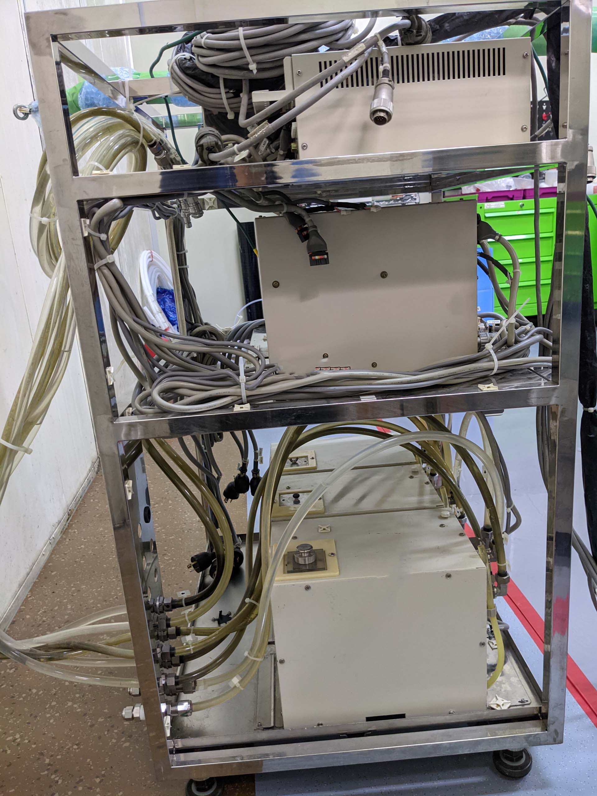


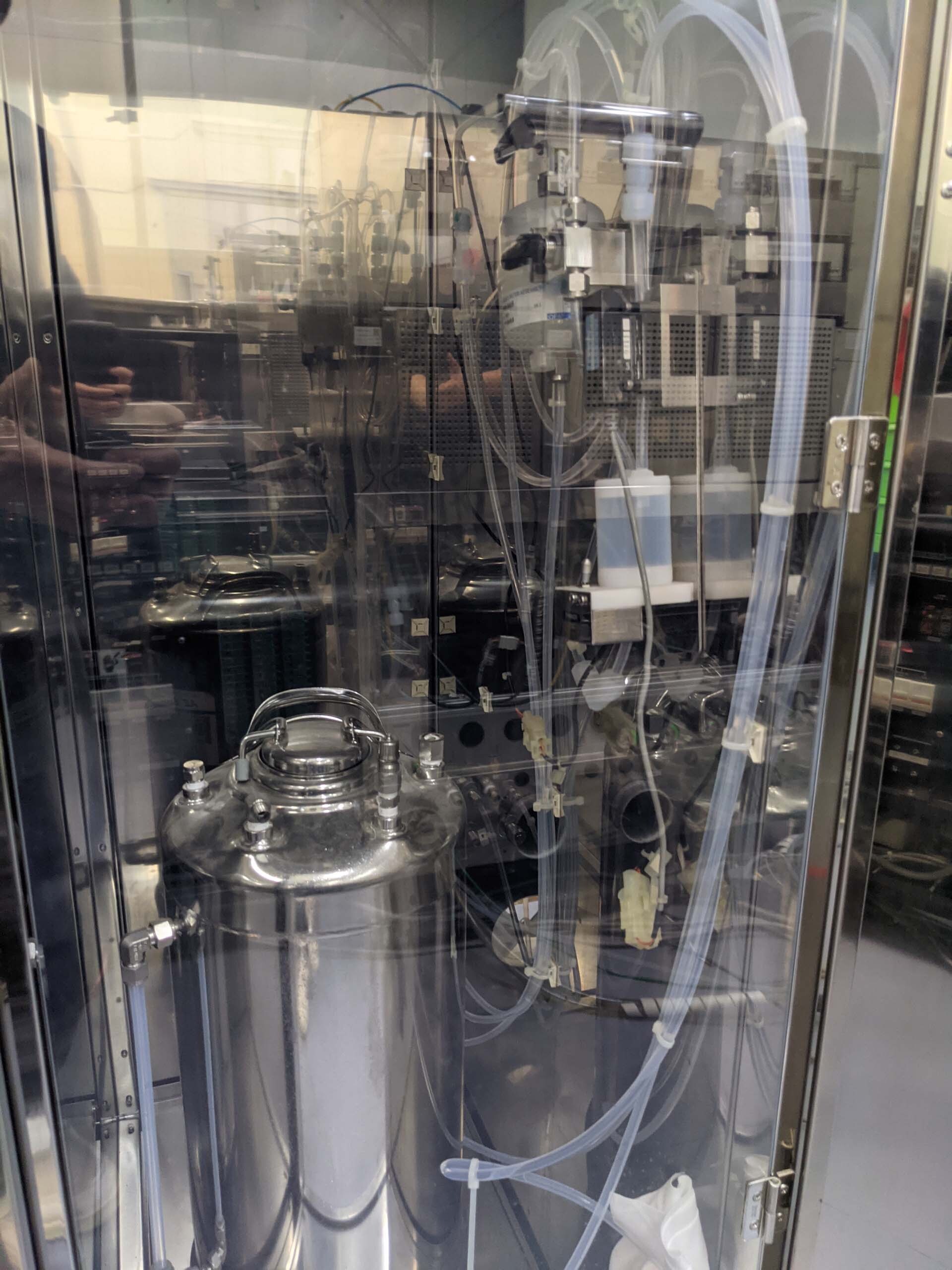

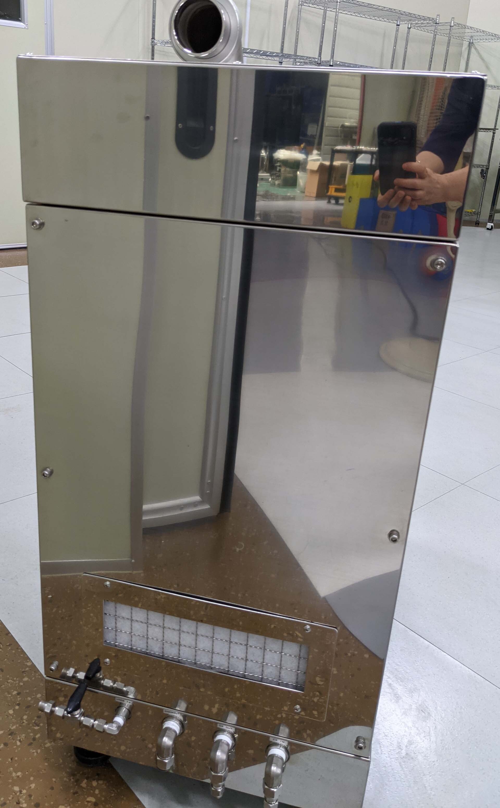

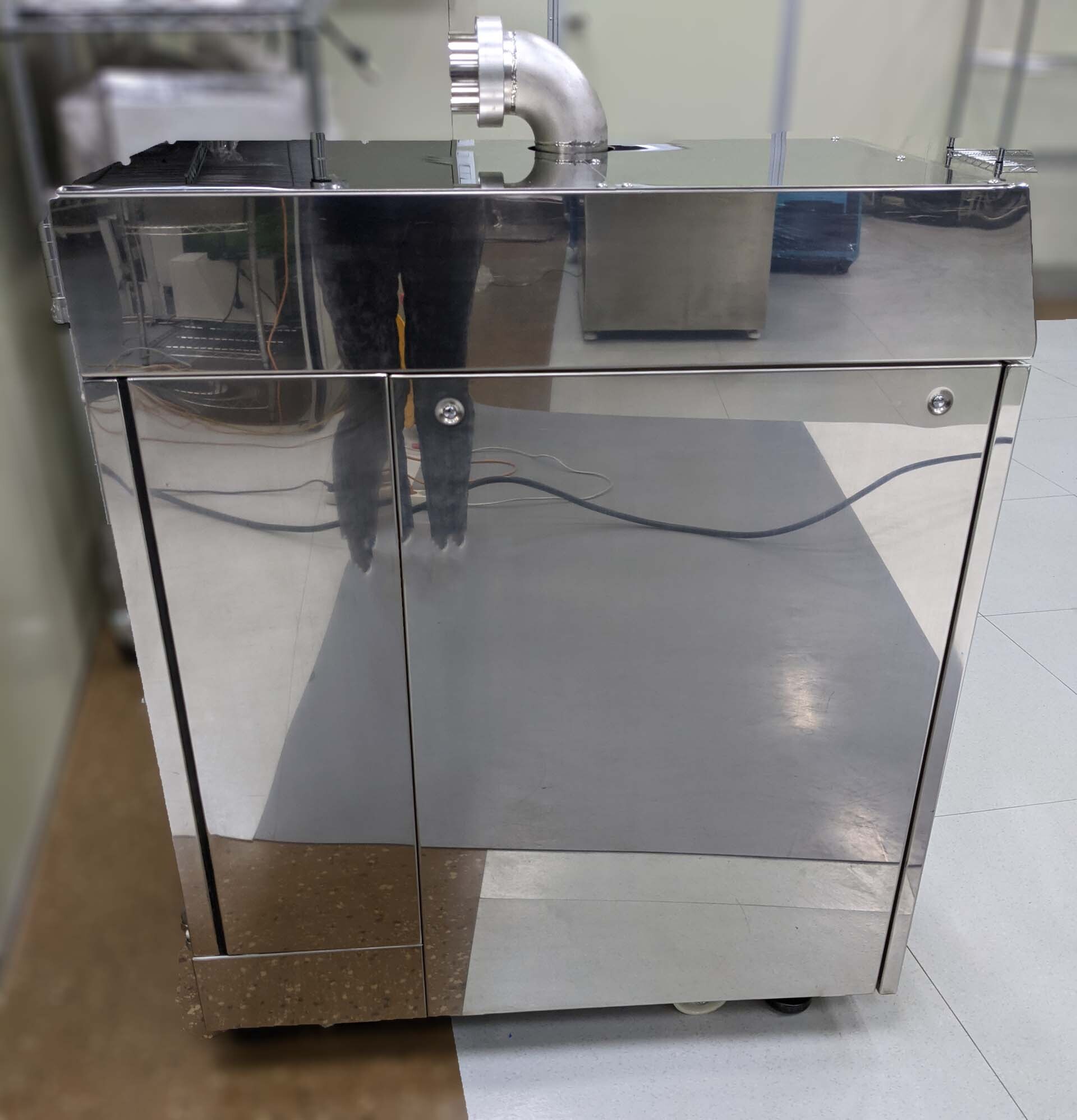















ID: 9386549
Wafer Size: 6"
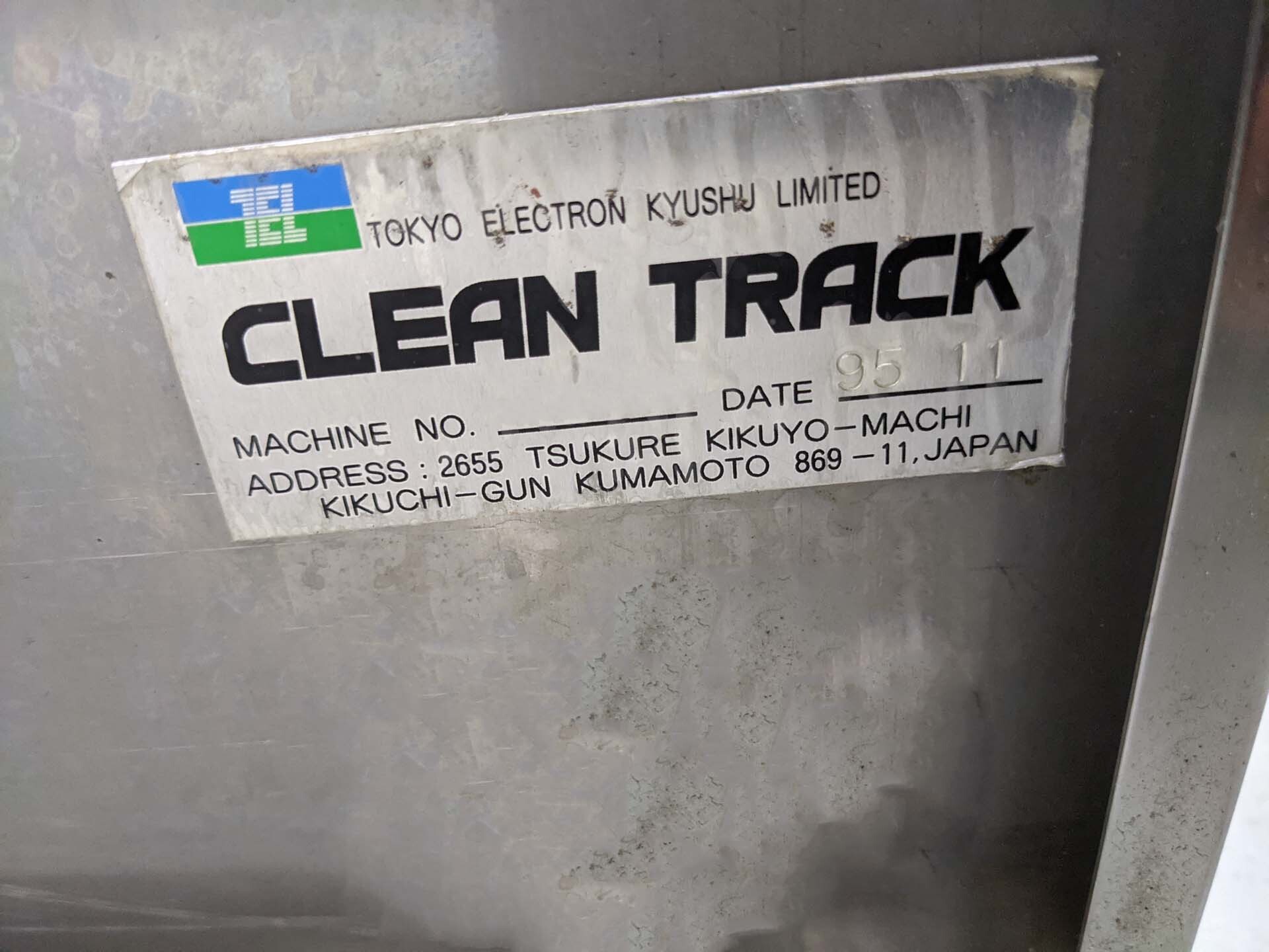
Vintage: 1995
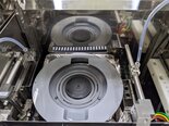
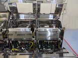
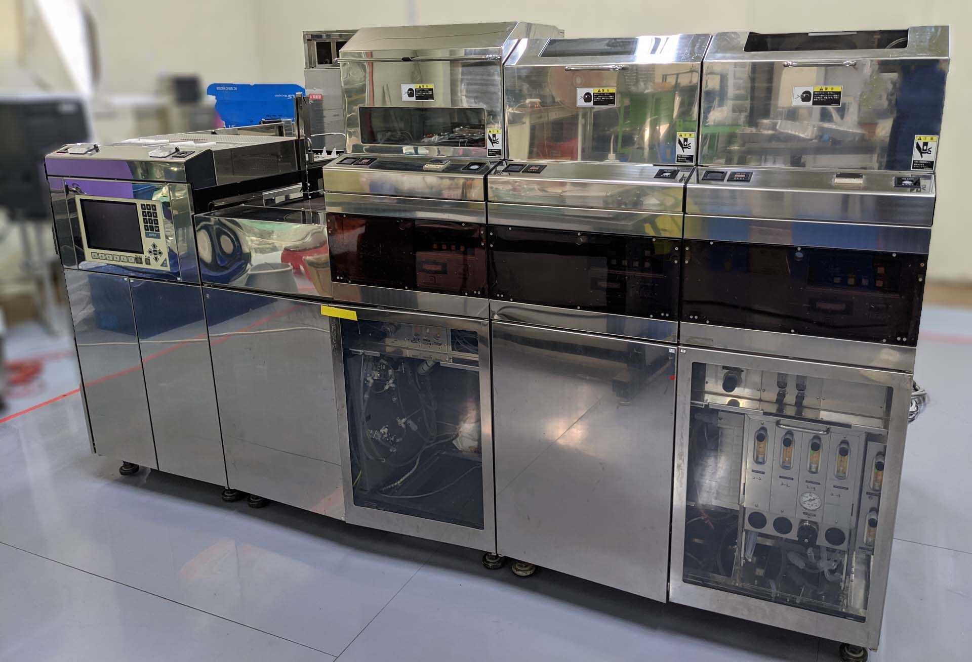
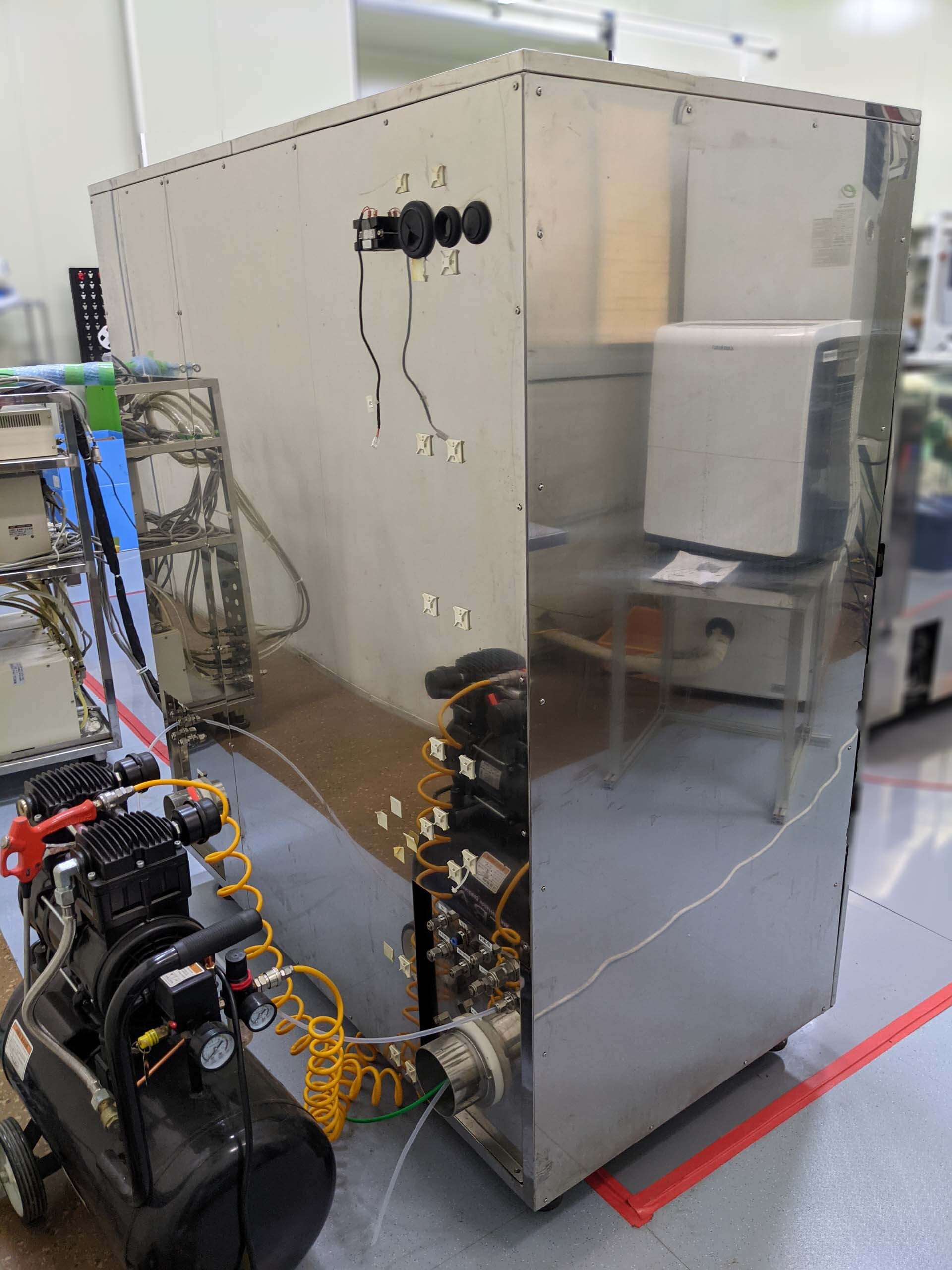
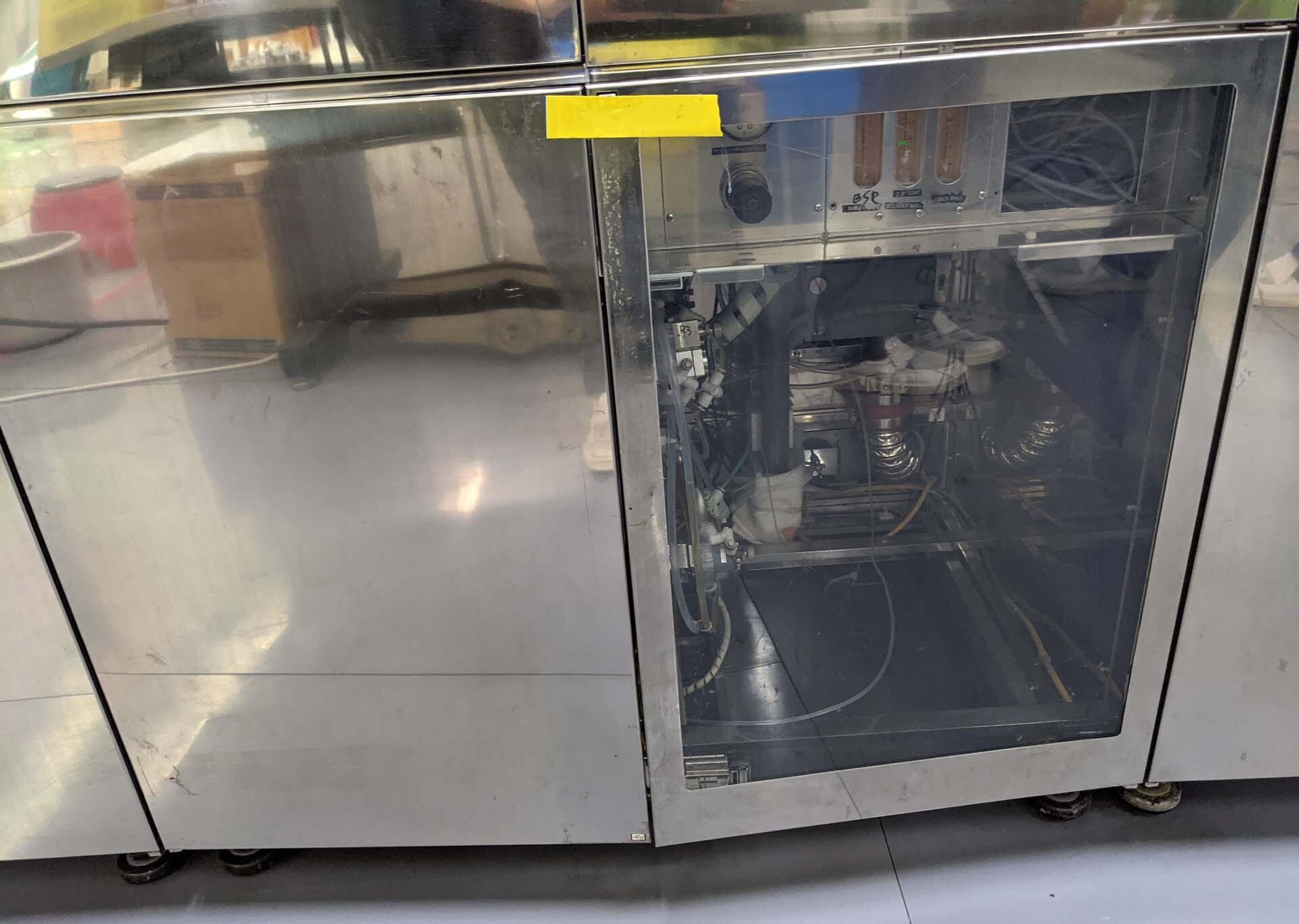
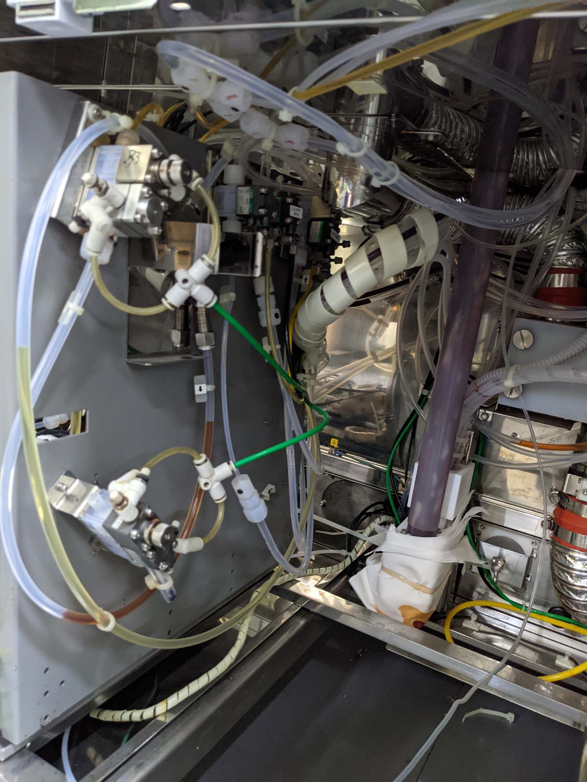
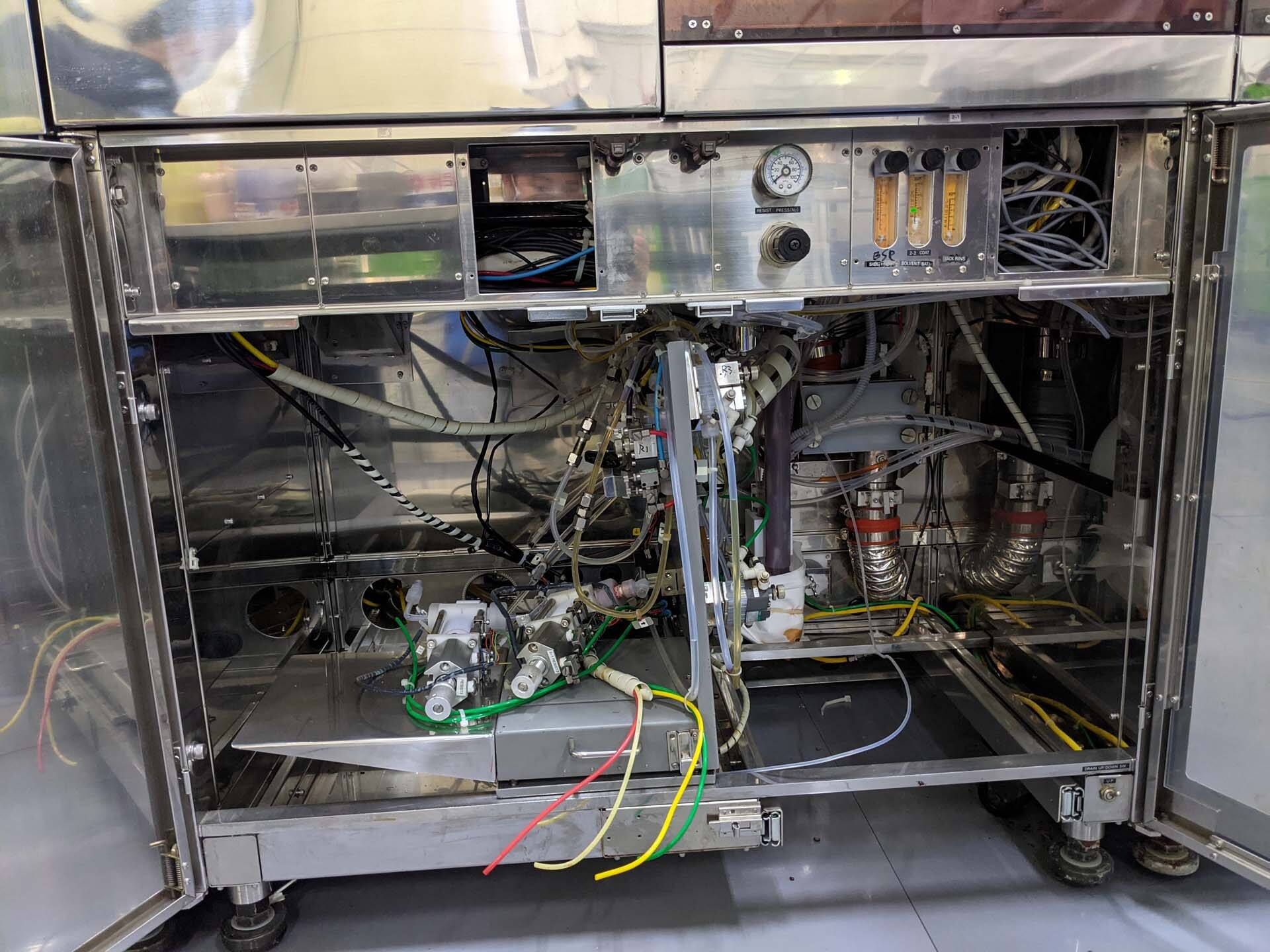
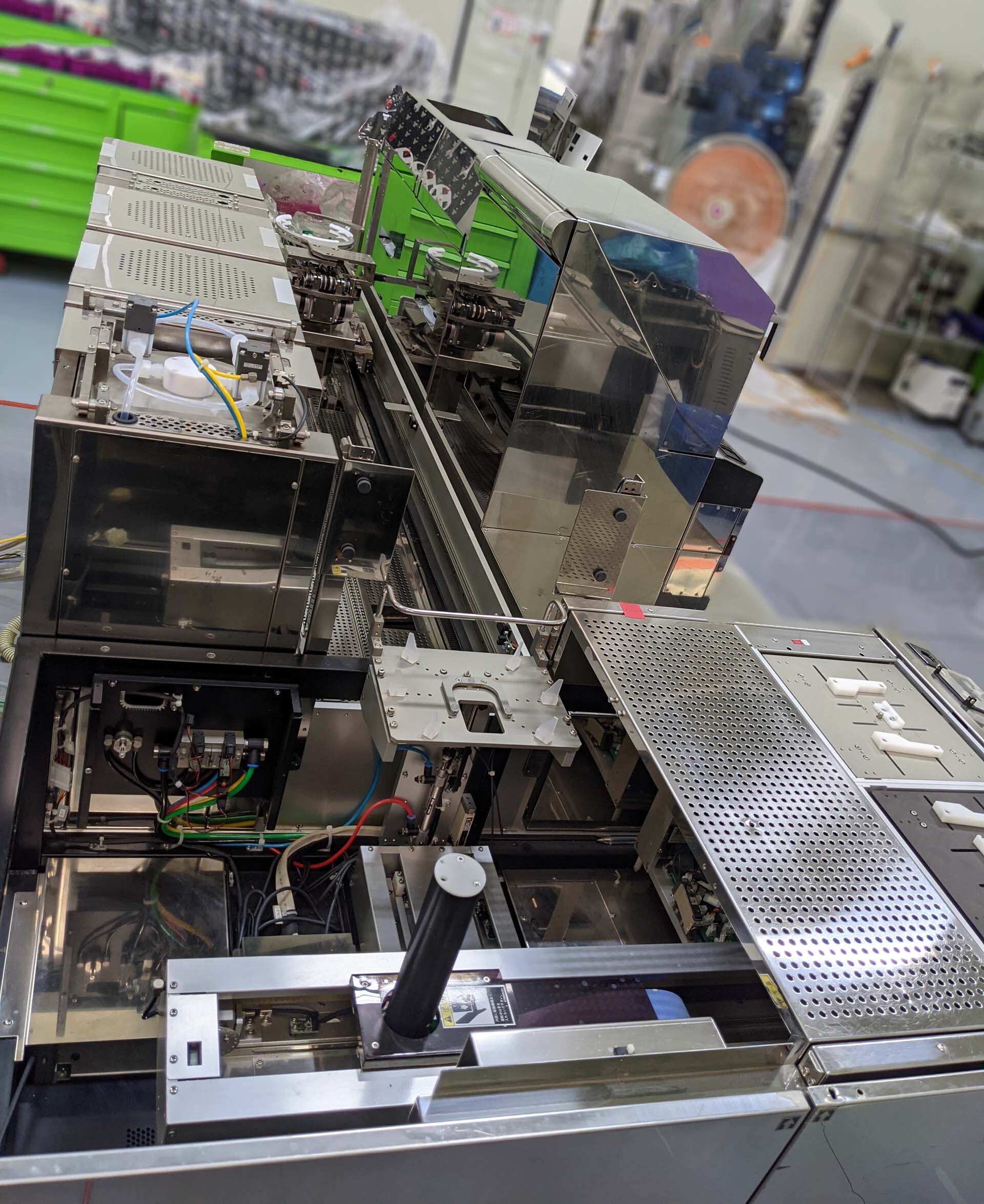
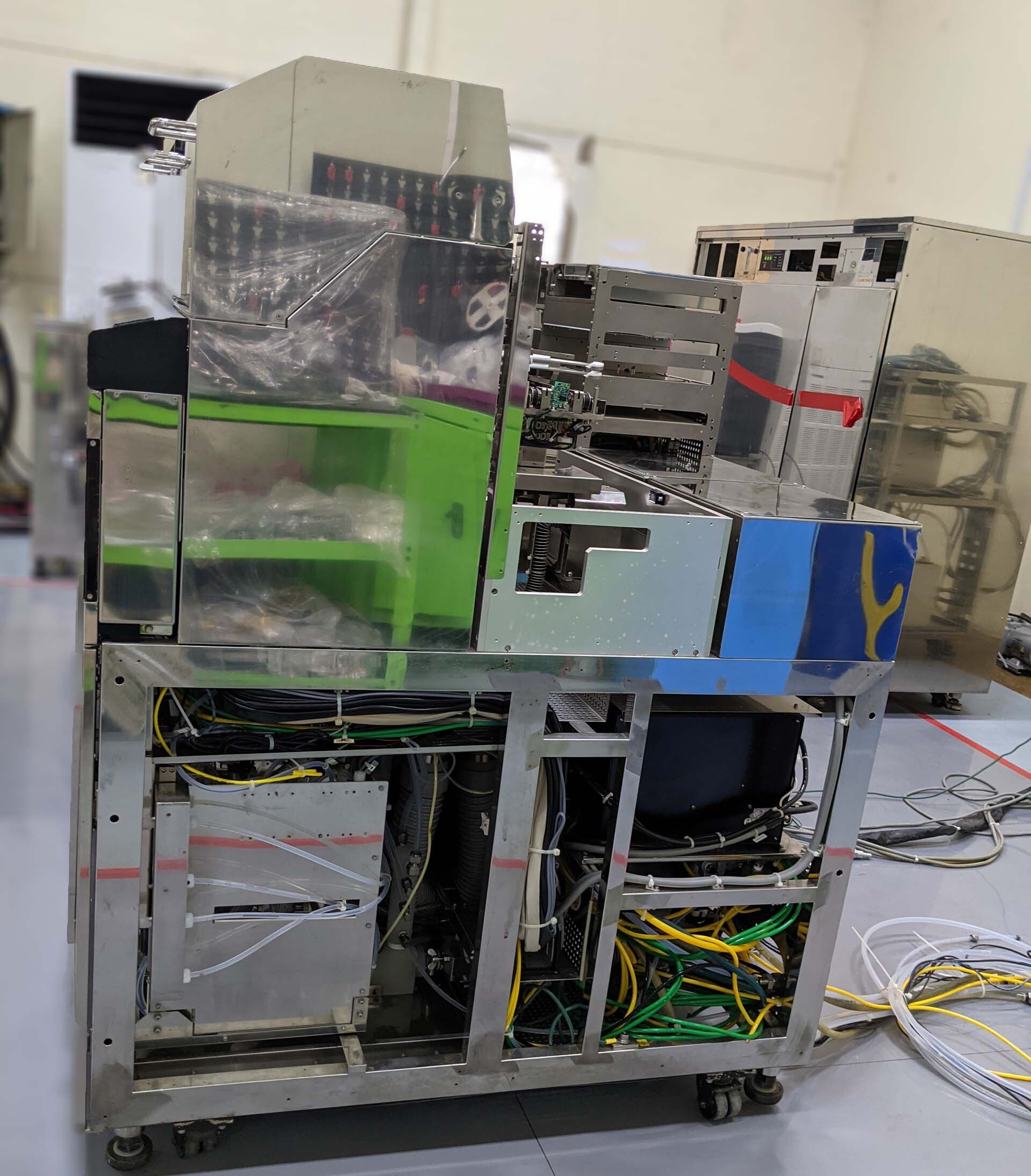
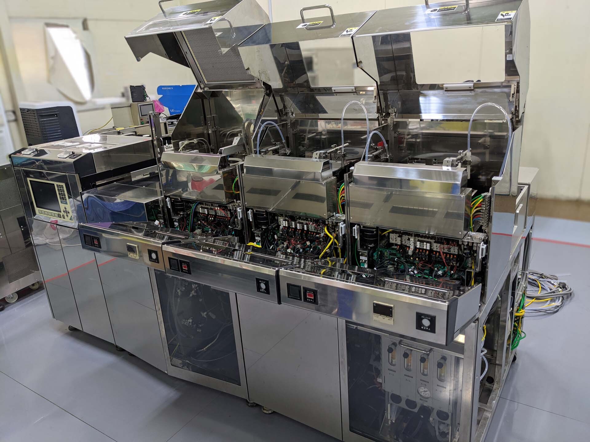
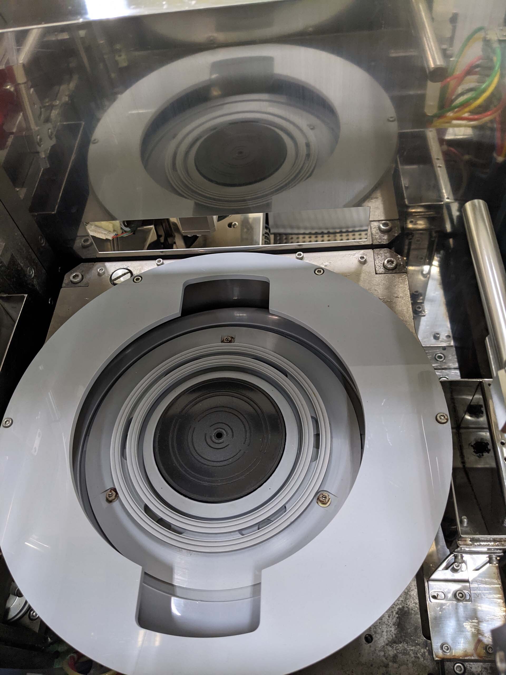
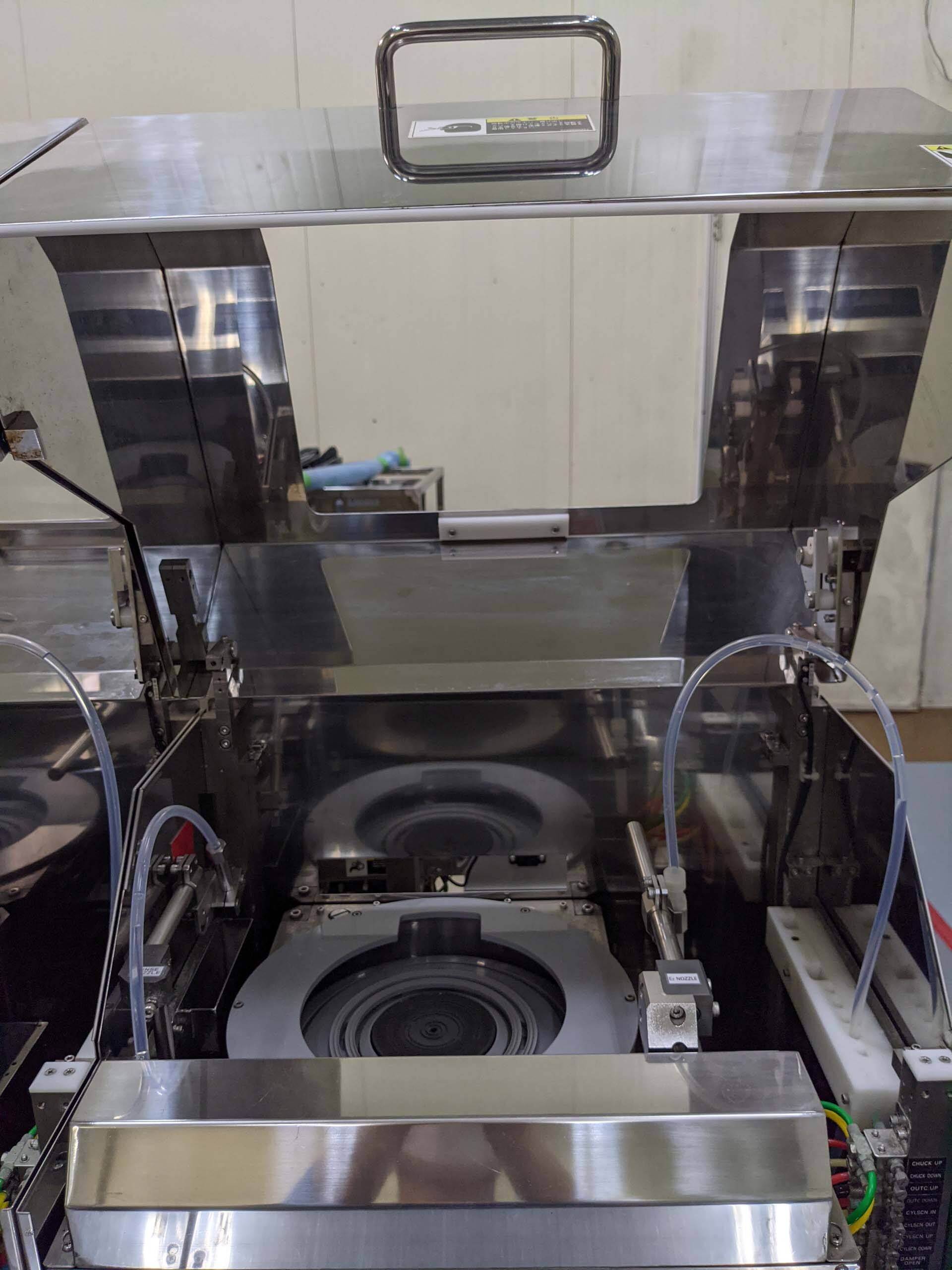
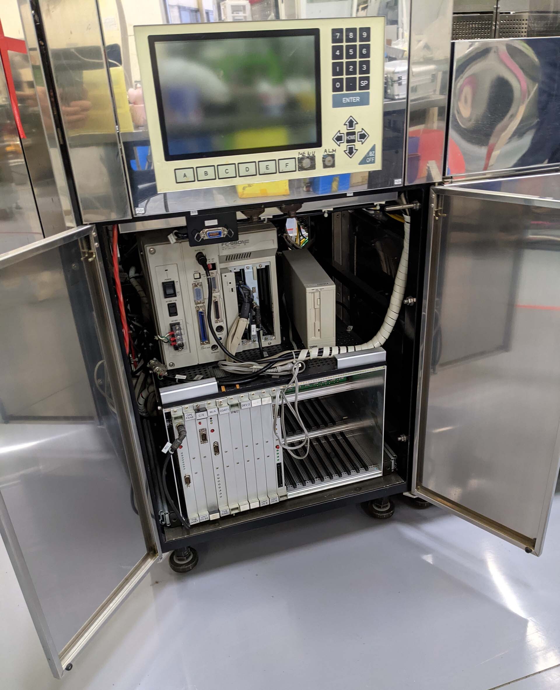
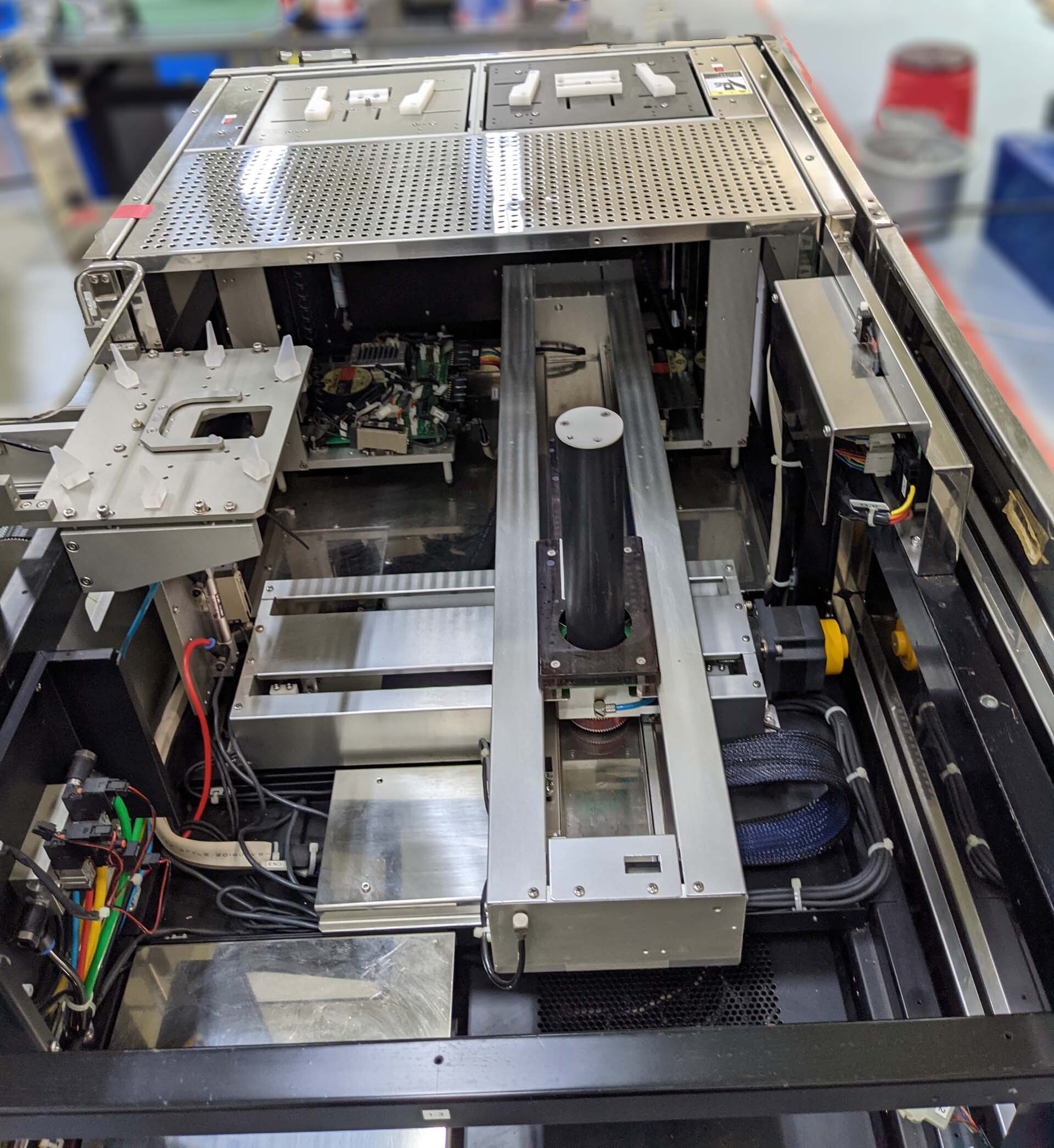
(1) Coater / (2) Developer system, 6"
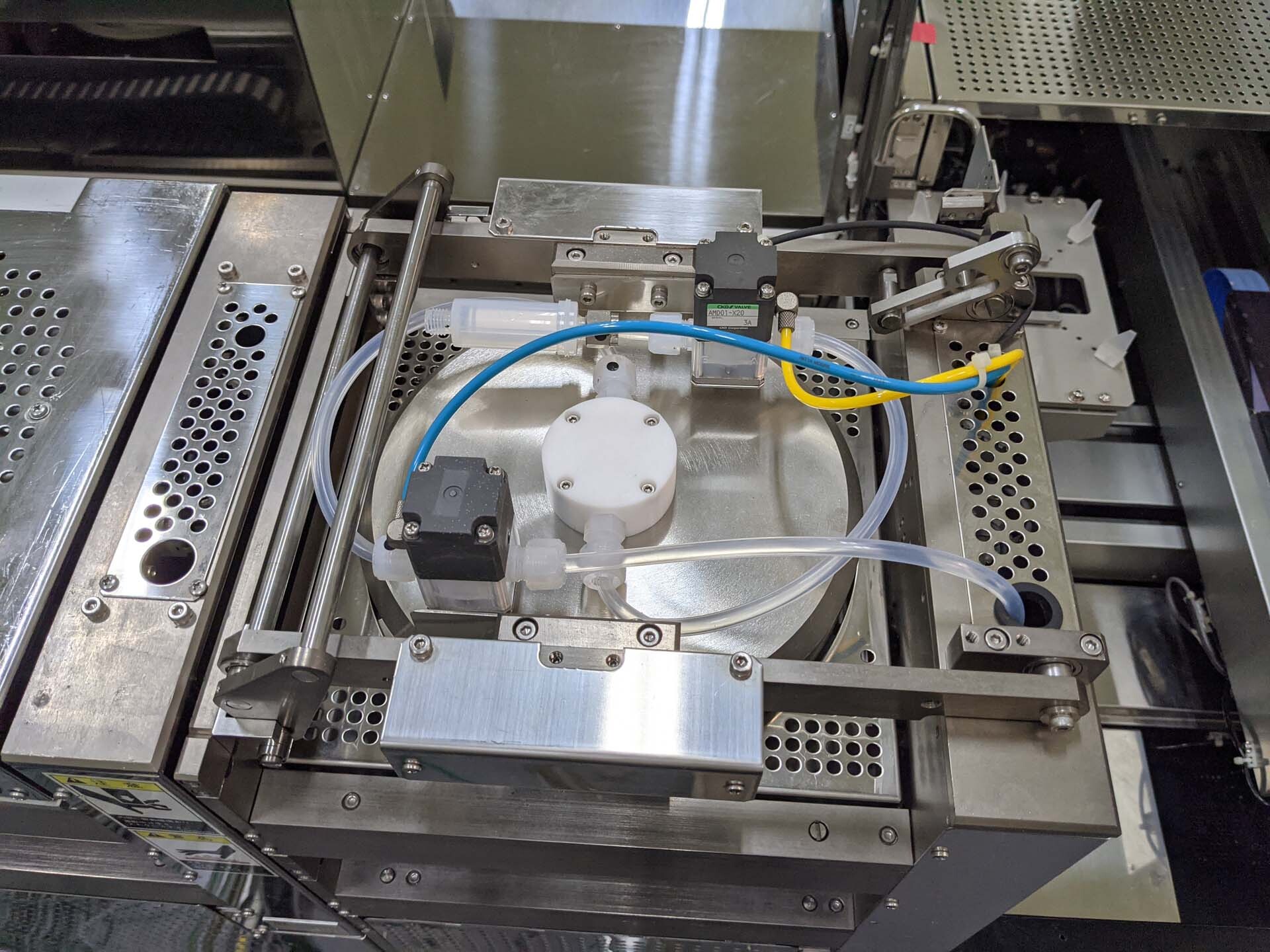
(4) Spin bodies
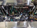
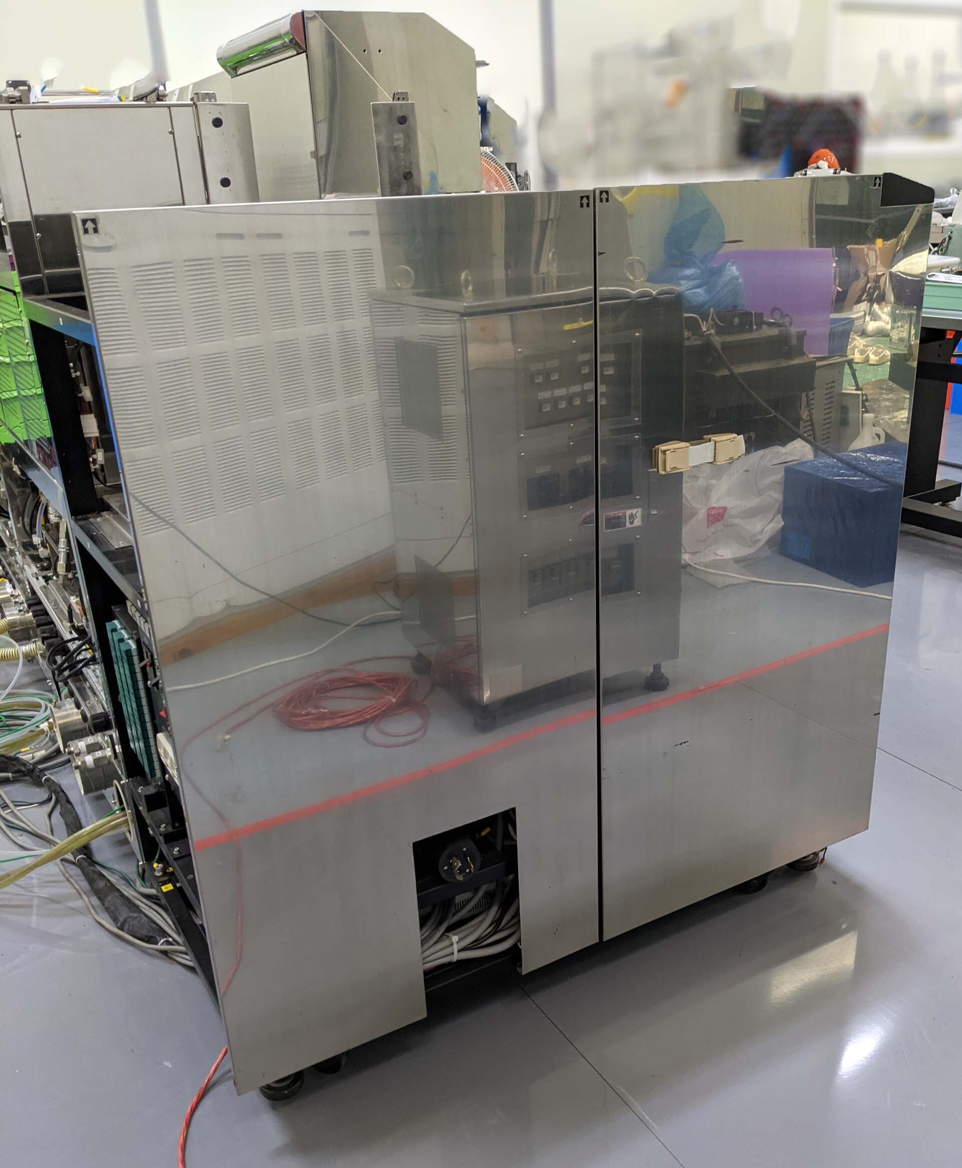
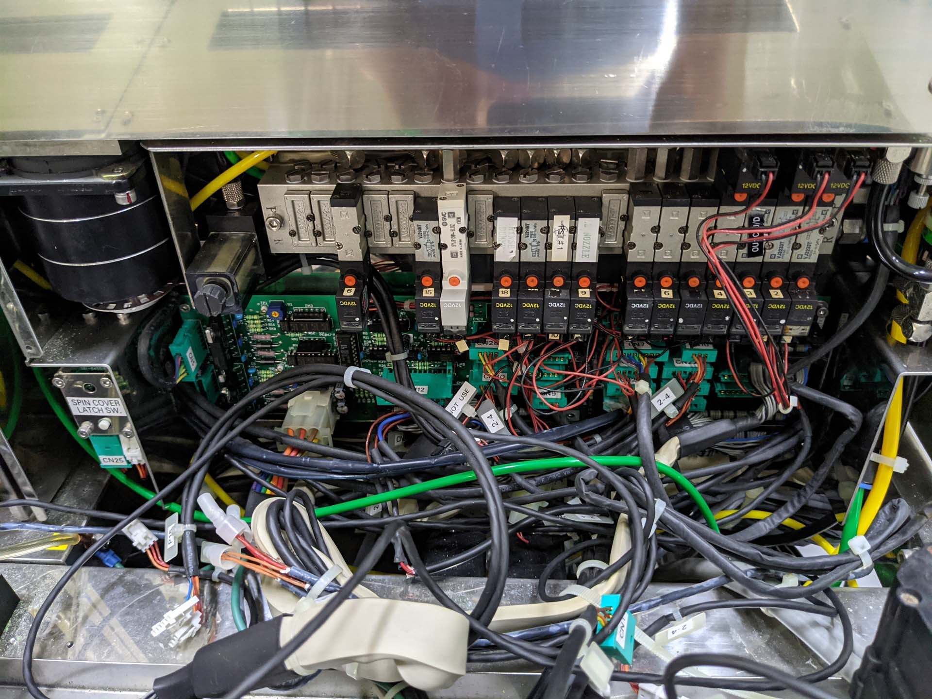
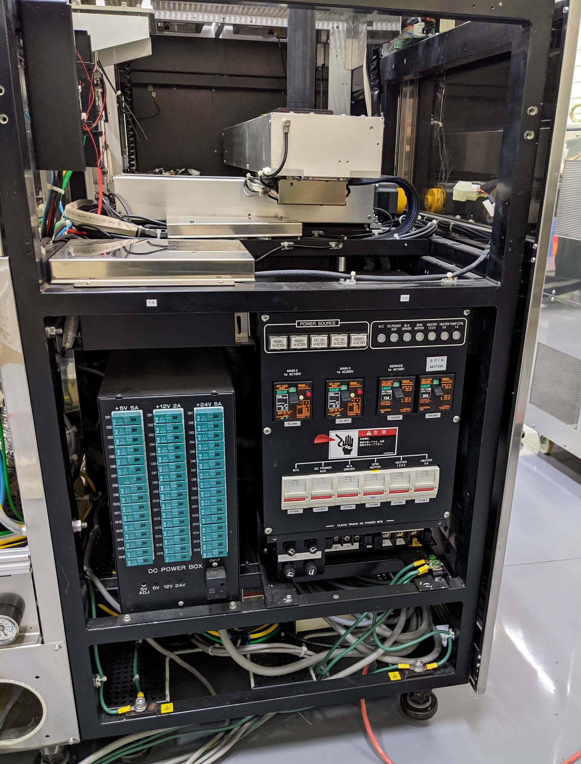
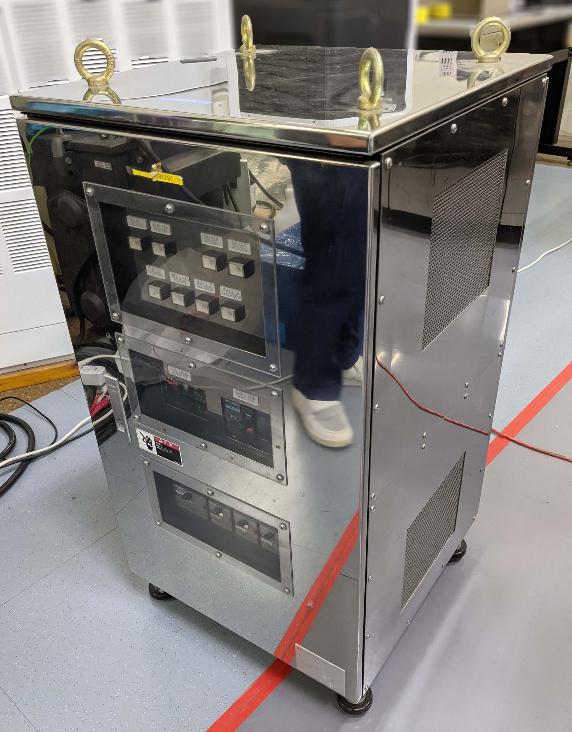
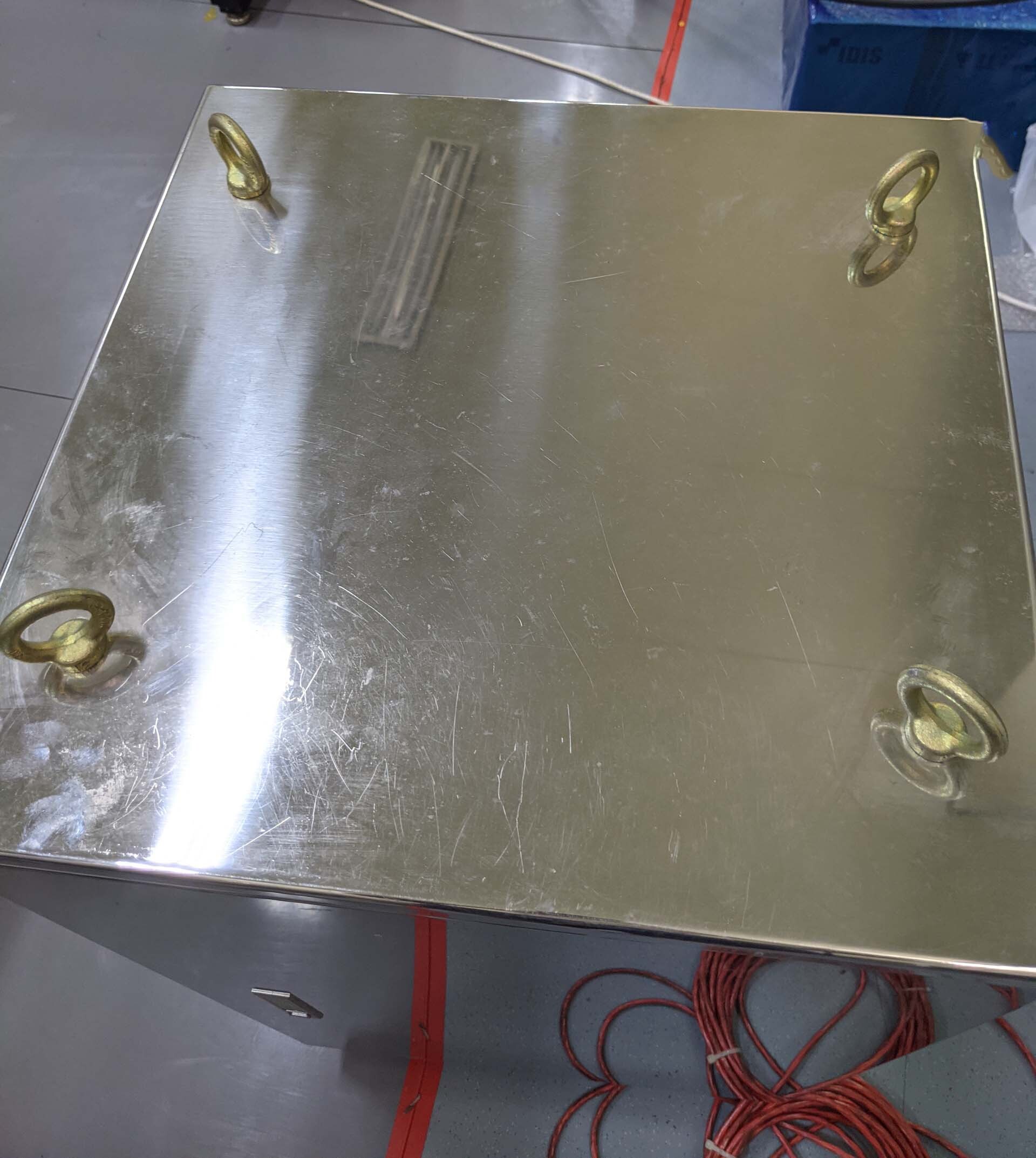
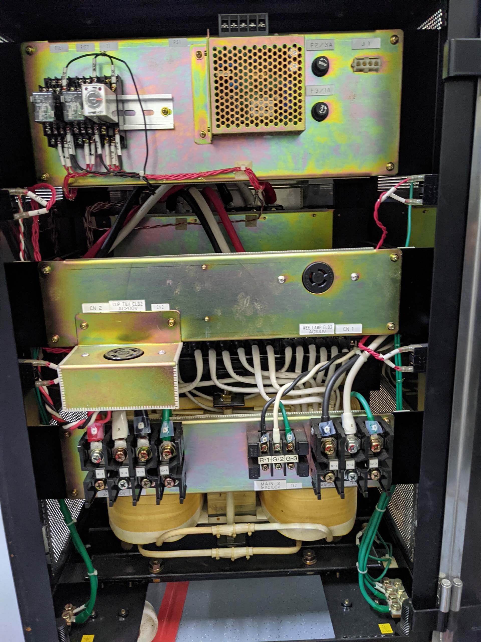
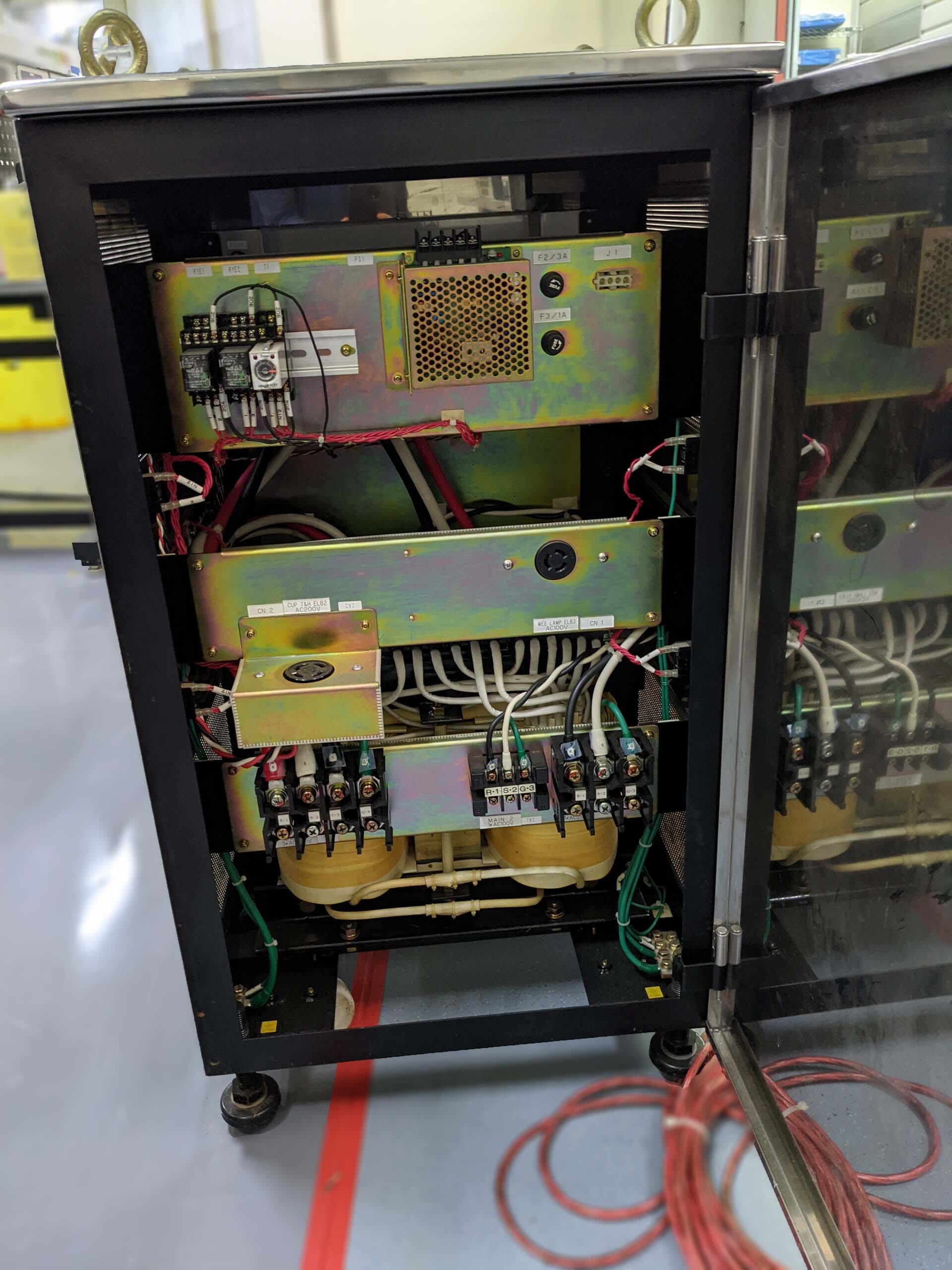
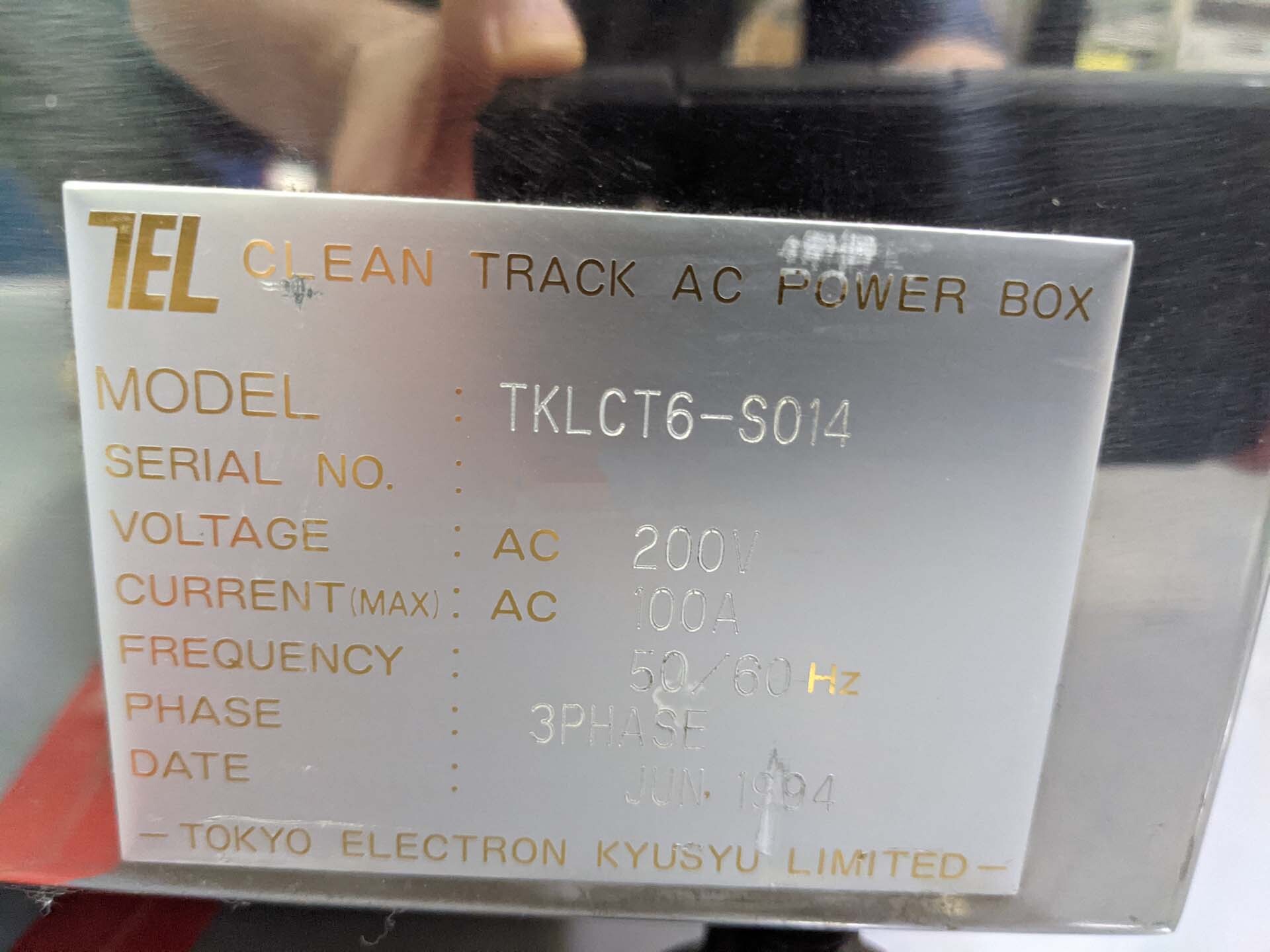
Power box
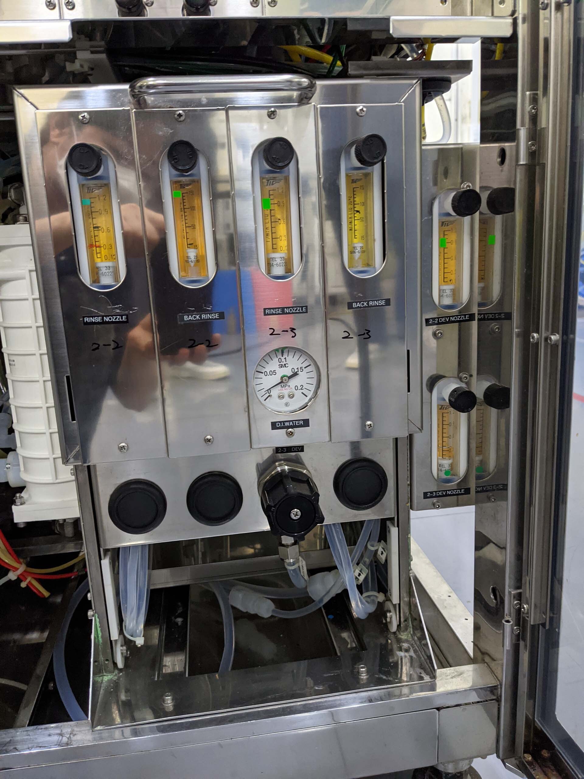
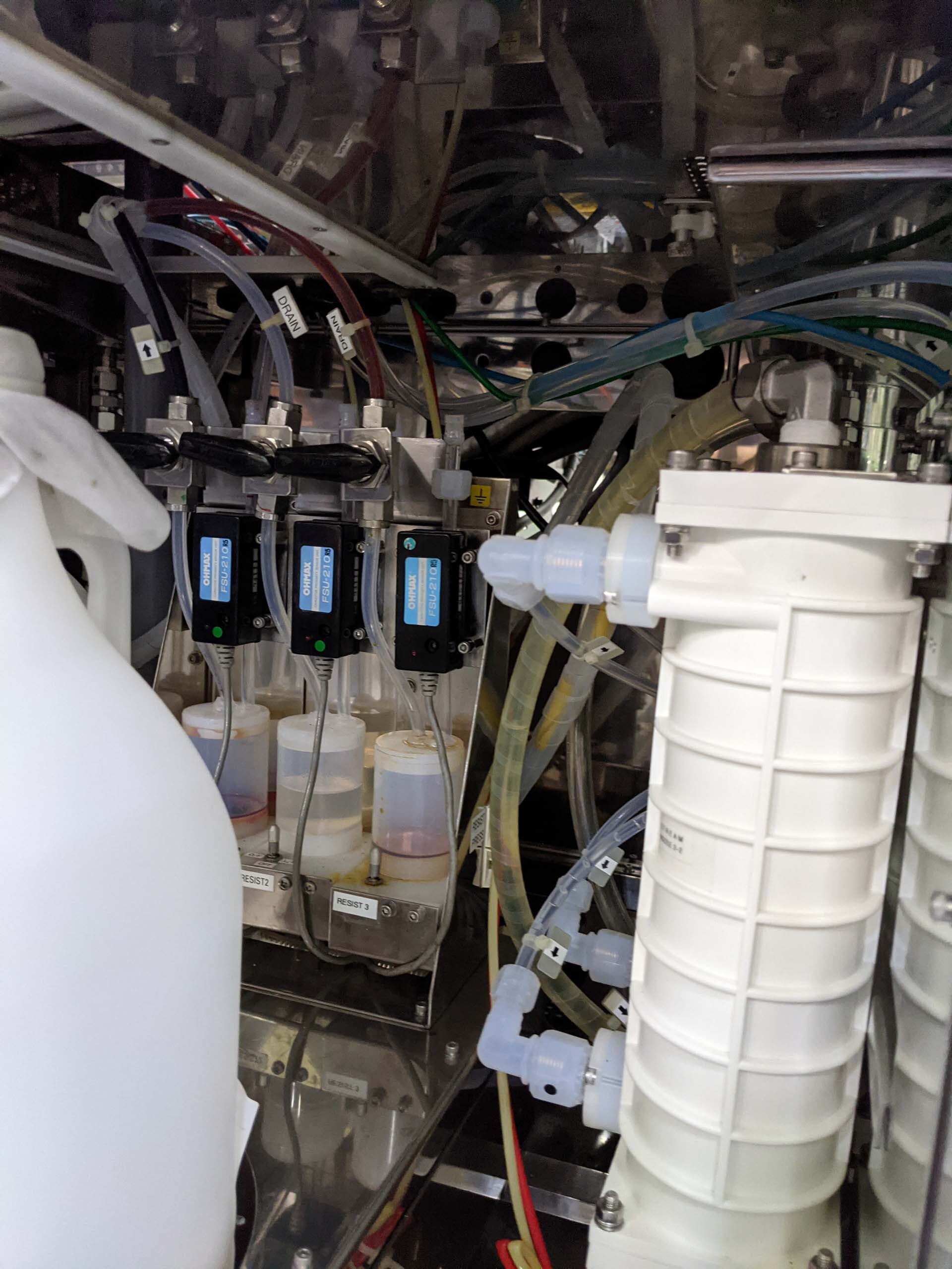
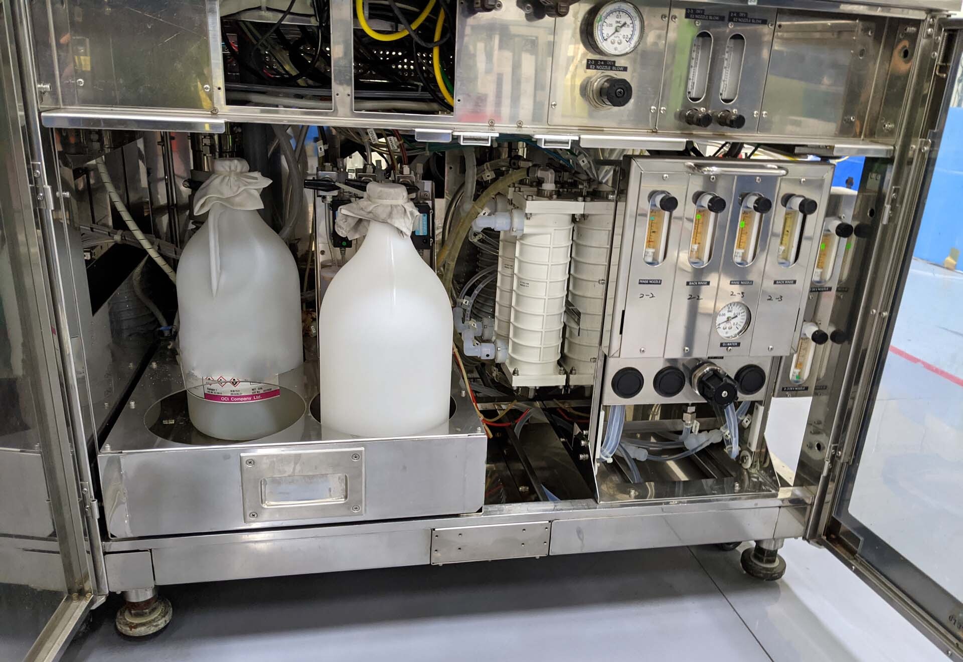
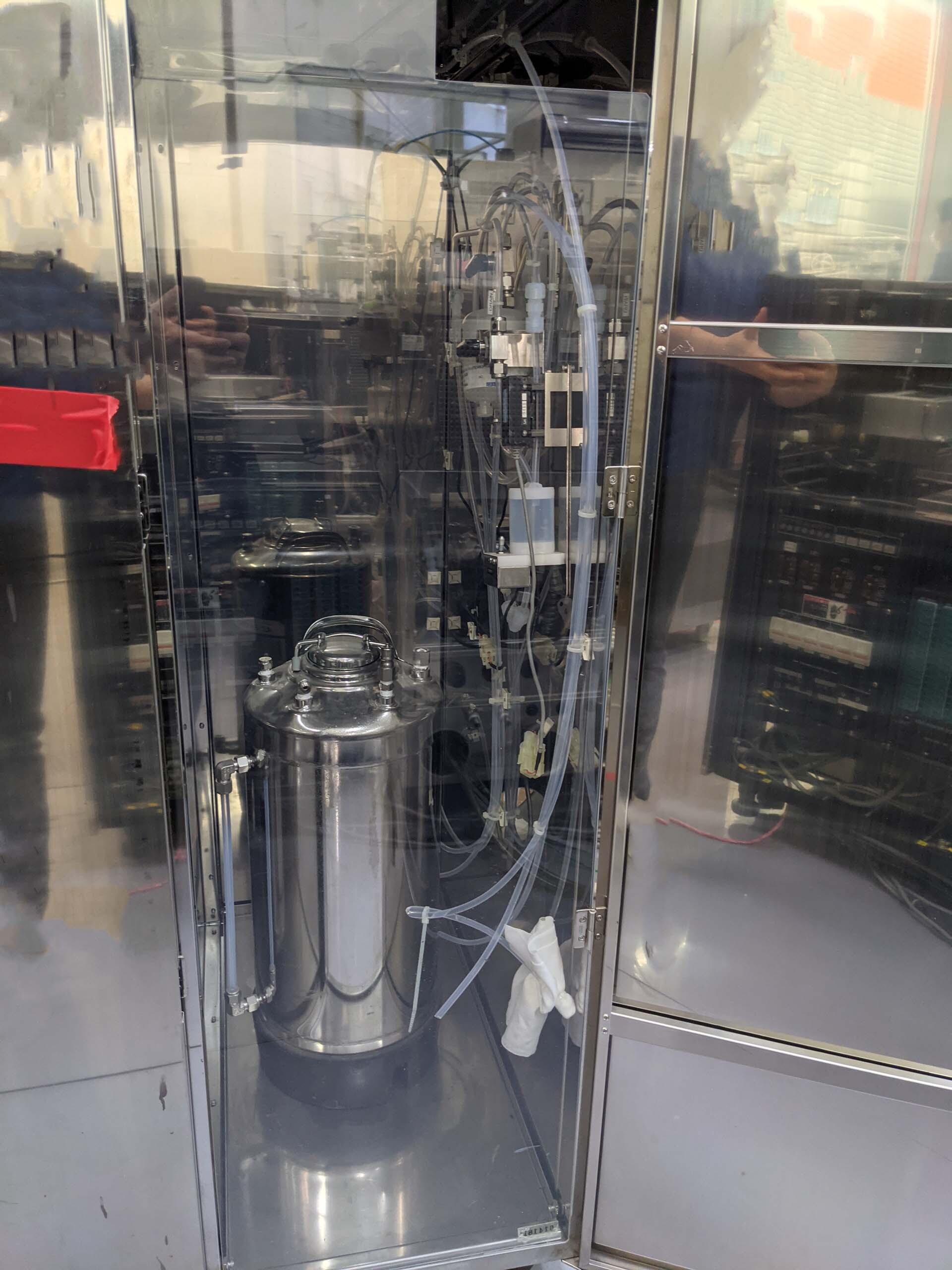
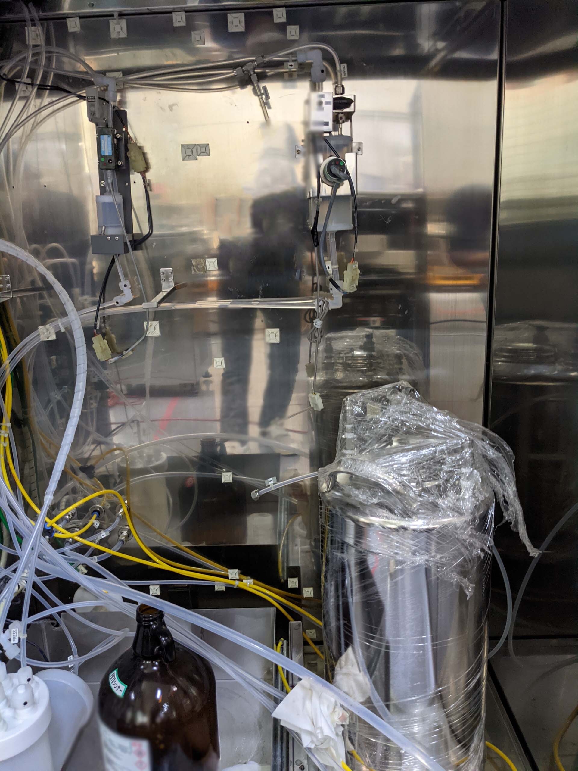
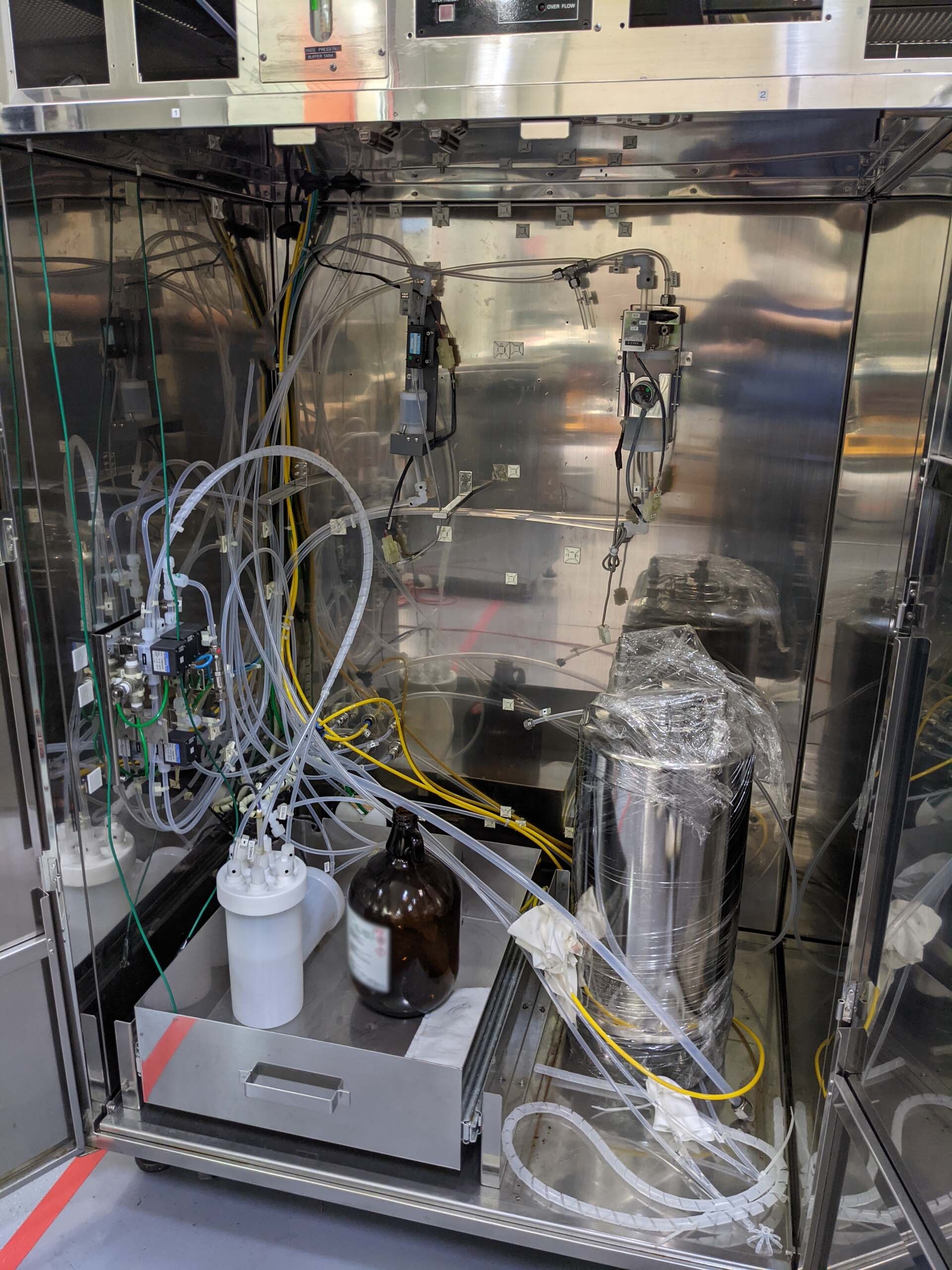
Chemical box
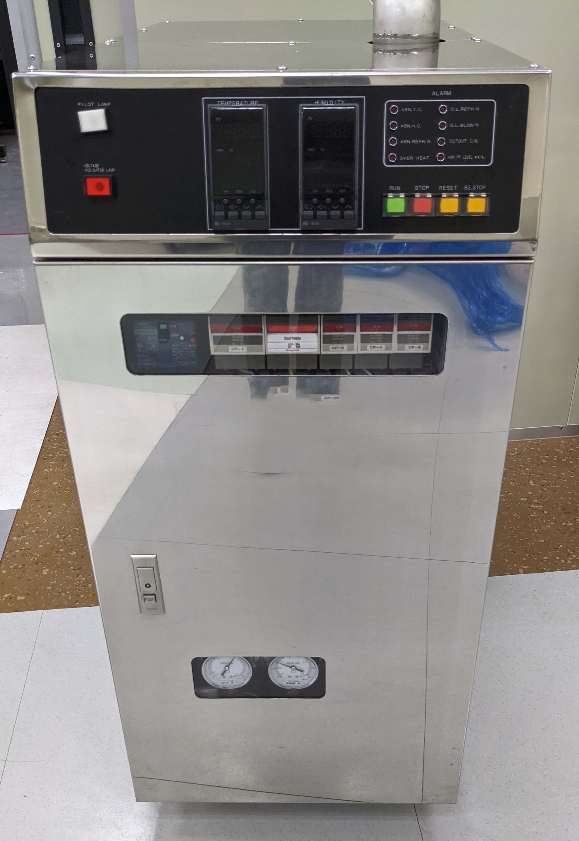
Temperature control unit
T and H (Auxiliary part)
Chuck, 6"
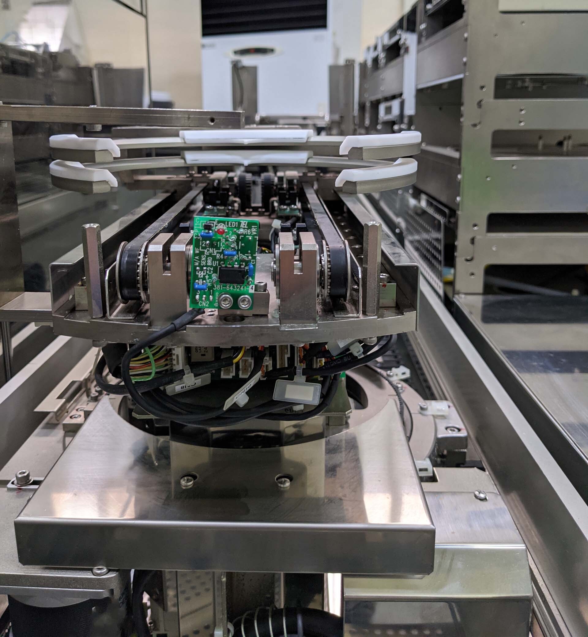
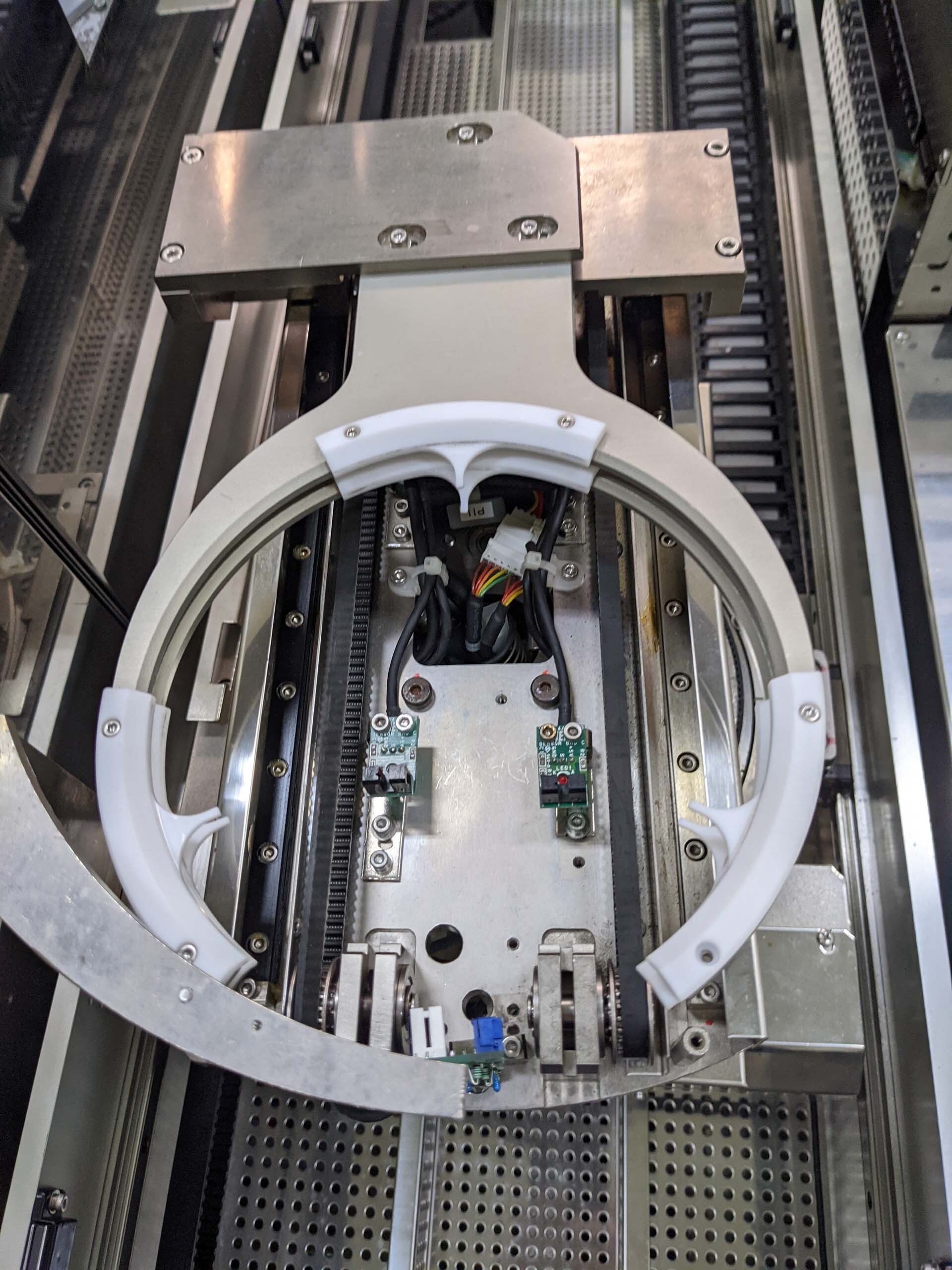
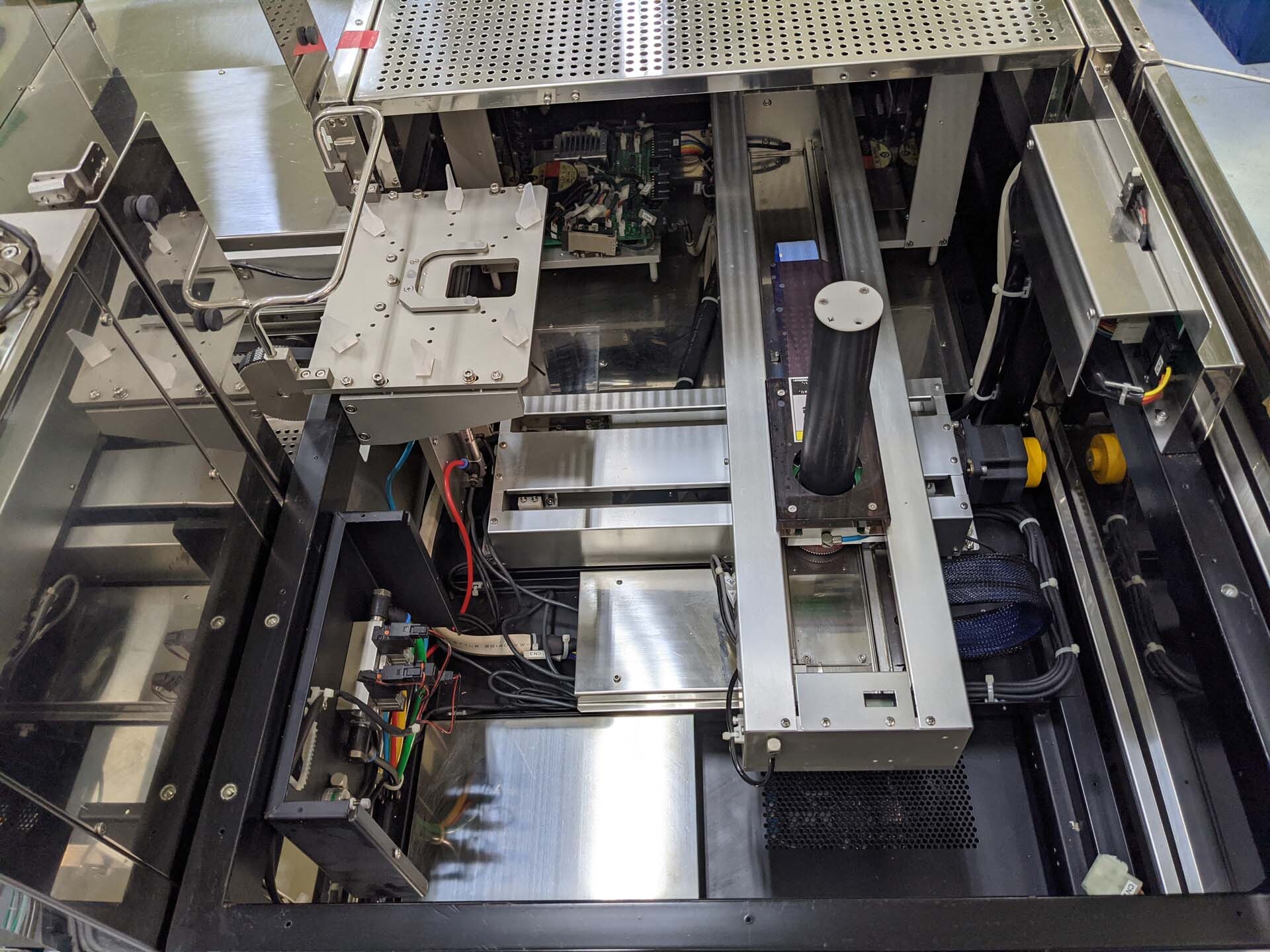
Transfer arm
Centering alignment
Index:
(2) Load ports
25-Slots mapping
Spin coater:
(2) Resist nozzles
PR Nozzle temperature control
Dummy dispense system
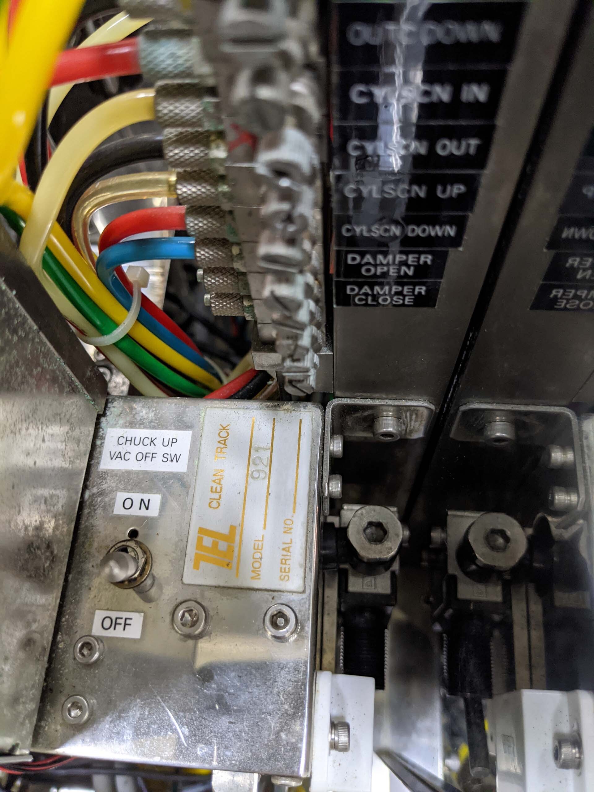
Vacuum chuck
Resist suck back
Back rinse nozzle
EBR Nozzle rinse
IWAKI Bellows pump
EBR Back flow meter
Upper and lower cup
Exhaust: Auto damper
Facility drain line
Nozzle moving: Stepping motor
Temperature and Humidity Controller (THC) Coater chamber
Spin motor:
AC Servo motor: 0-5000 RPM, ±2 RPM
Maximum: 5000 RPM
(2) Spin developer:
Develop nozzle temperature control
Vacuum chuck
DI Rinse
Back rinse nozzle
Upper and lower cup
Developer flow meter
Back rinse nozzle
DI Rinse
(4) Hot plates, 6"
PID
PT Temperature sensor
Program time: 0 ~ 990 sec (set 1sec)
Temperature range: 50°C - 180°C
(3) Cooling plates, 6"
PID
PT Temperature sensor
Range: 15°C - 35°C
AD Plate, 6"
PID
PT Temperature sensor
HMDS Vapor chamber cover
HMDS Bubbling tank
Program time: 0 - 990 sec (set 1sec)
Temperature range: 50°C - 180°C
Chemical cabinet:
Photo resist system
Bottle (1 Gal): Trap tank, (2) Nozzles
HMDS Tank: 2.5 L
Thinner: Canister (5 GL)
Developer: Canister (5GL)
1995 vintage.
TEL / TOKYO ELECTRON MARK Vz is a photoresist equipment that features top-of-the-line positive and negative photoresist technology. This system makes it possible to develop resists for a variety of applications, especially those involving high-resolution, semiconductor-compatible design. The patented TEL MARK-VZ can precisely form patterns in the nanometer range. The unit features a substrate holder that allows samples of any size to be placed on the platform. Its coverage area is sufficient to accommodate huge wafers, and substrate stage accuracy ensures positioning accuracy. TOKYO ELECTRON MARK V-Z also includes an exposure head, with a Nobel-prize-winning Gaussian illumination beam and adaptable focus position. This allows for greater accuracy and optimal exposure consistency. In lithography, the PATMAX feature of MARK V-Z guarantees pattern accuracy. It employs the latest evolutionary algorithms to produce the best possible results. The machine also includes features such as auto-calibration and auto-solving, which cut down on manual steps, working to reduce time and improve overall efficiency. Additionally, the dry highly-reflective illumination optics feature an Original HRI Supersymmetric Reflector (SHR), allowing for up to eighty-eight times more light energy than existing systems. This enables higher exposure resolutions and drastically decreases processing time. The optics also provide optimized uniformity, making MARK-VZ optimal for both advanced lithography and back end processes like wafer cleaning and etching. The tool integrates a CENTRAL software suite, which allows for easy control of the exposure process and access to the machine's settings. It also provides a 3D view for progress evaluation and enables advanced operations. Supporting the management of up to four exposure systems, CENTRAL ensures the highest exposure accuracy. This new photoresist asset from TEL utilizes the latest technologies and algorithms to attain remarkable precision and efficiency. With powerful dry optics and a software suite for advanced control, MARK Vz may be the ideal photoresist model for the most demanding semiconductor applications.
There are no reviews yet
