Used TEL / TOKYO ELECTRON system #293770373 for sale
URL successfully copied!
Tap to zoom
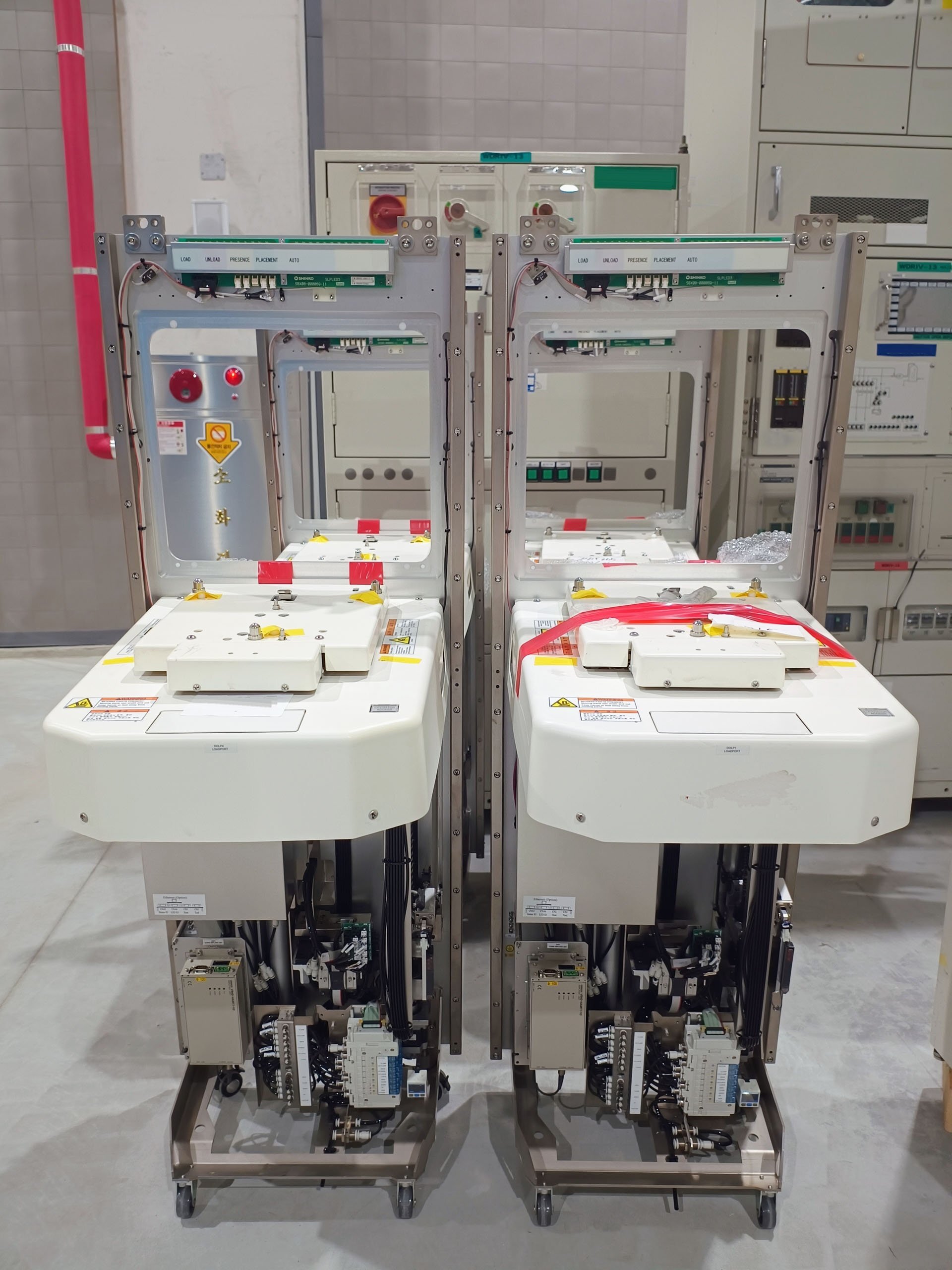

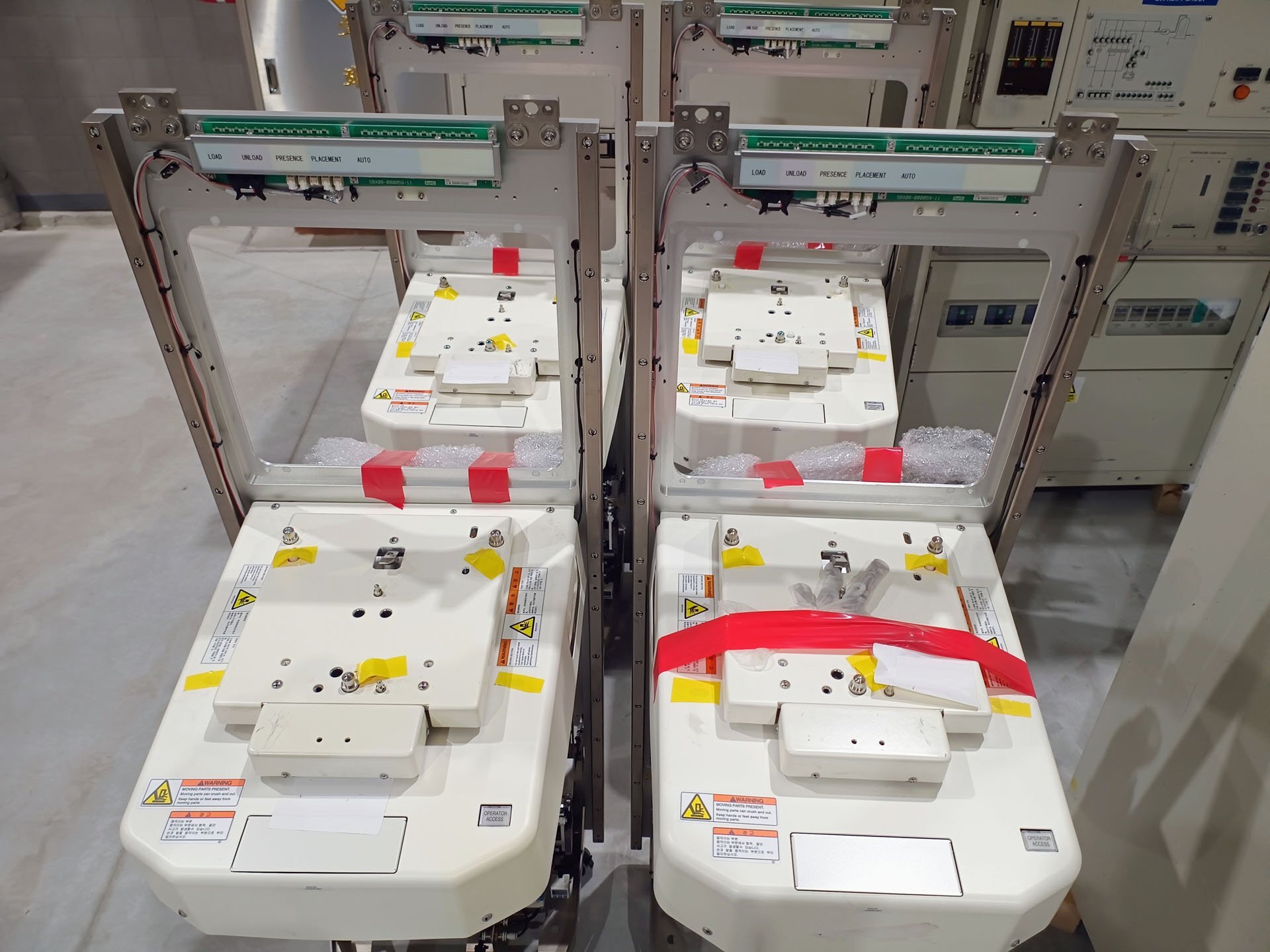
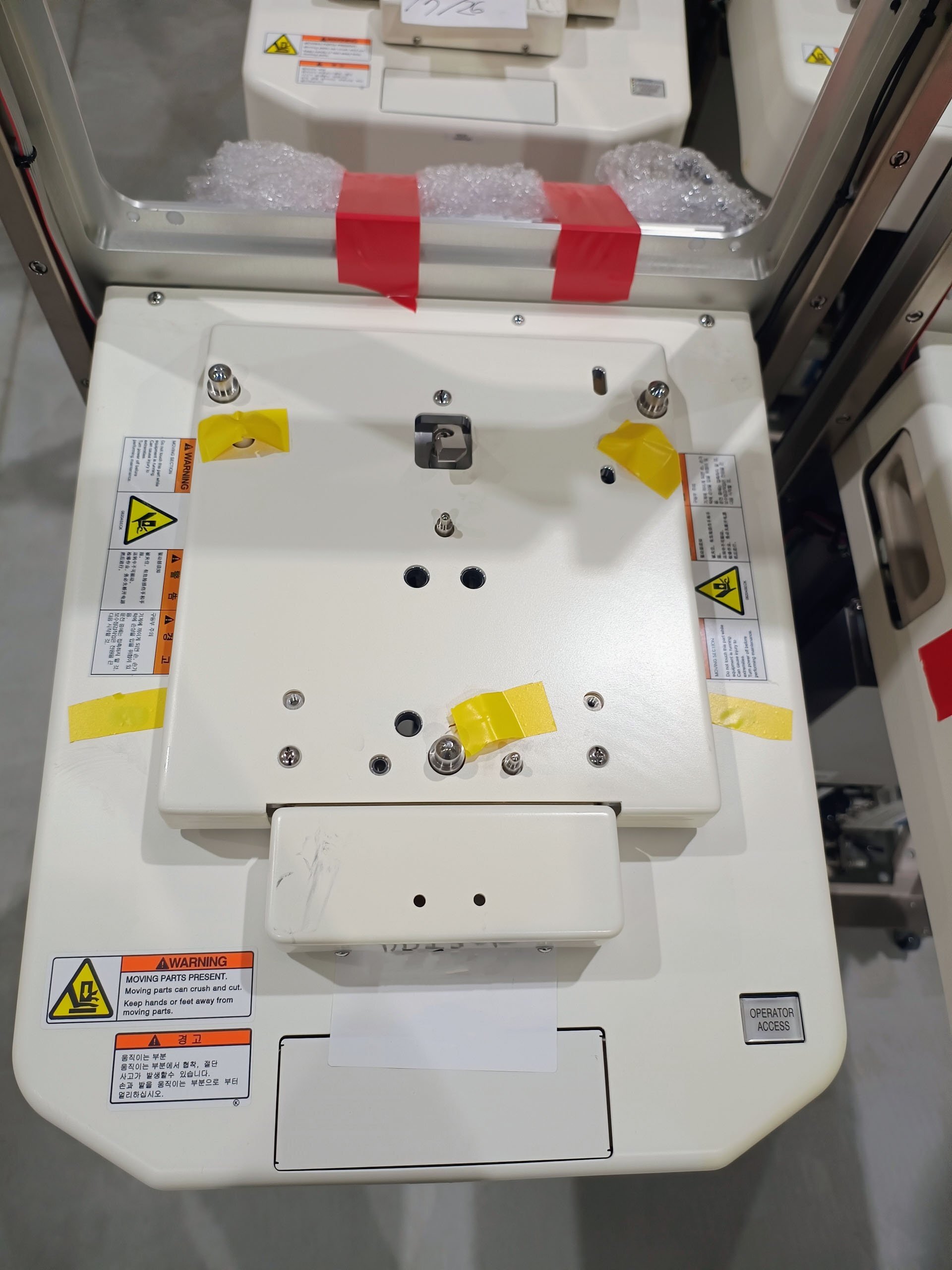
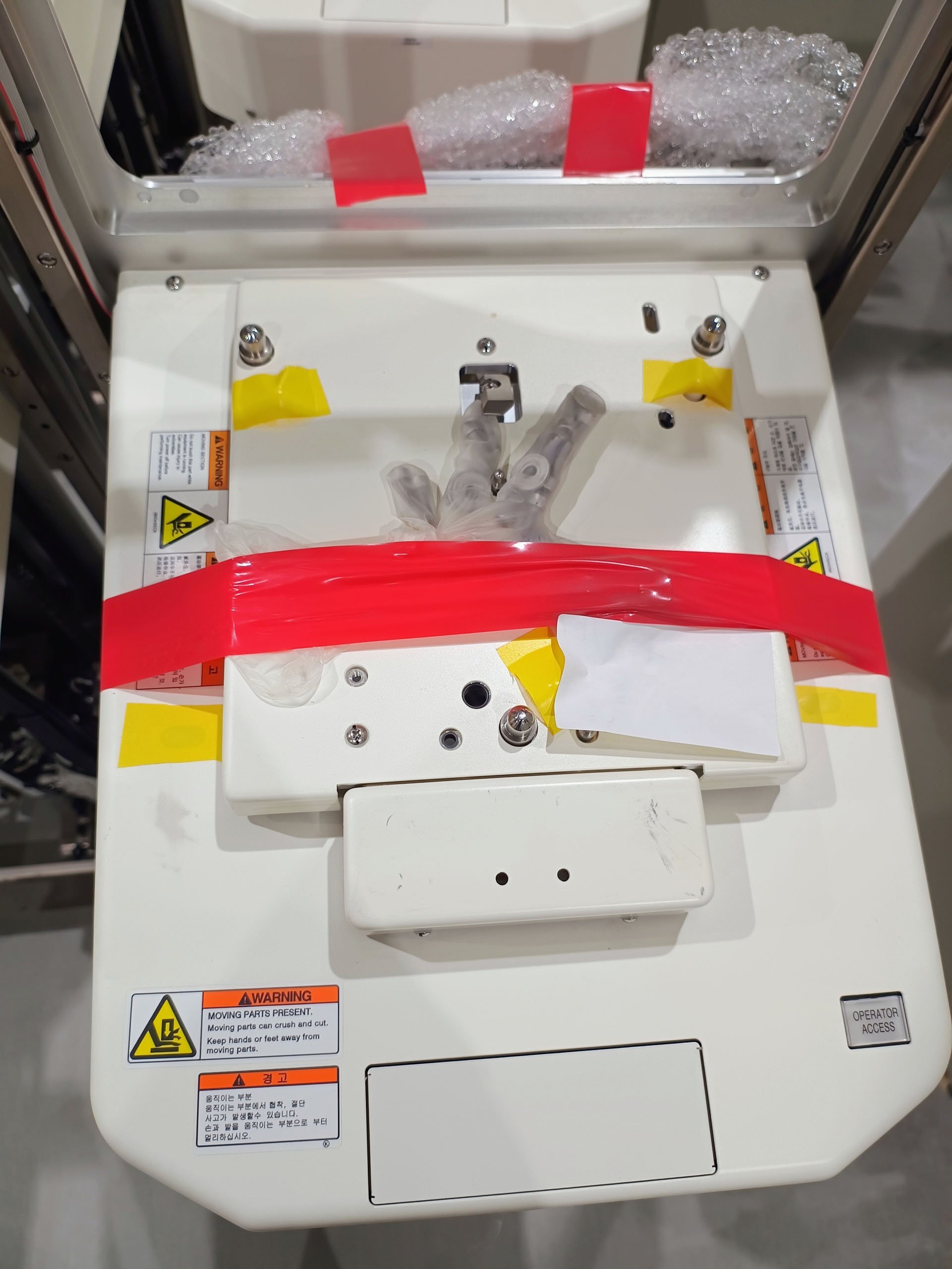
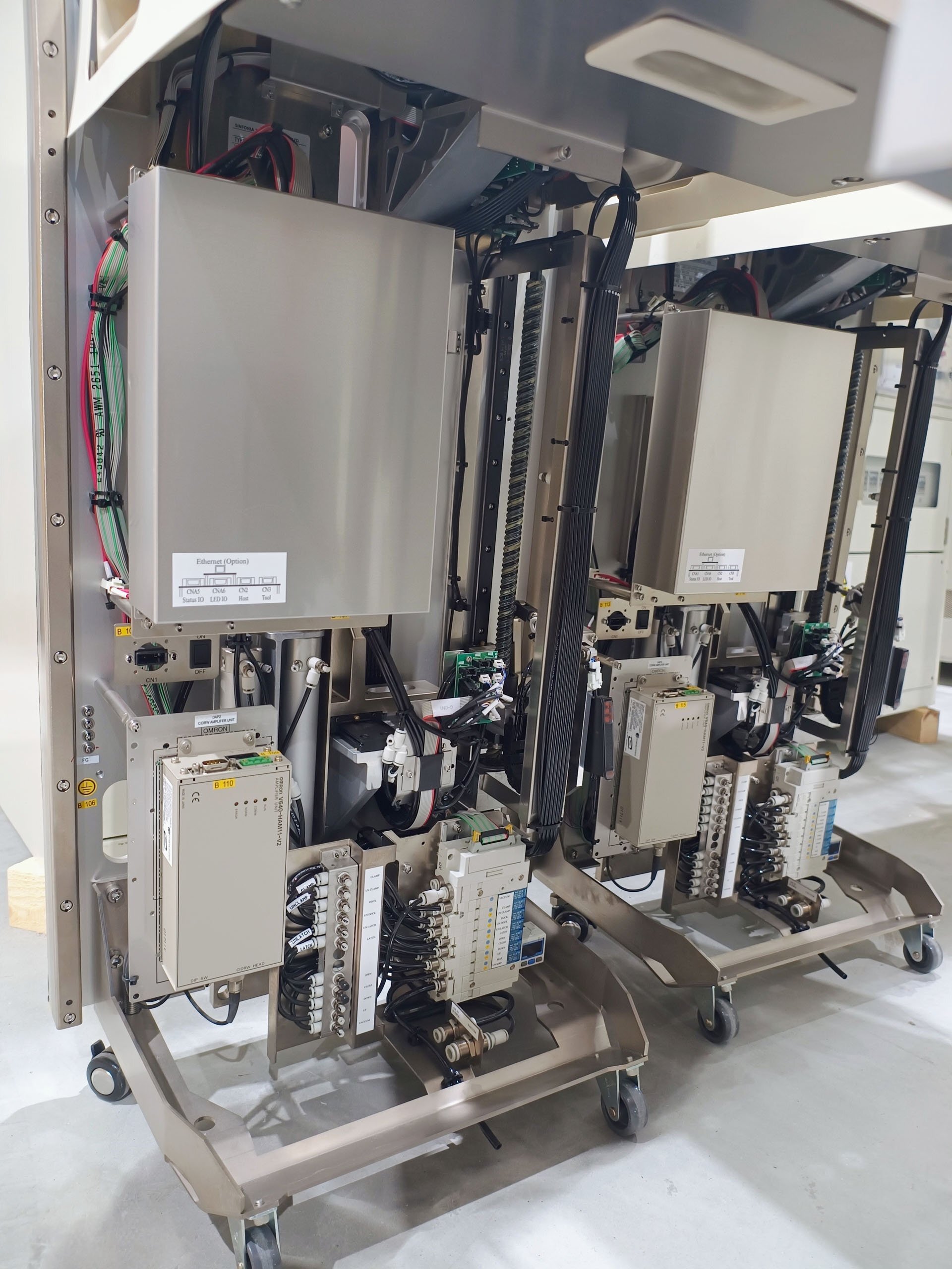
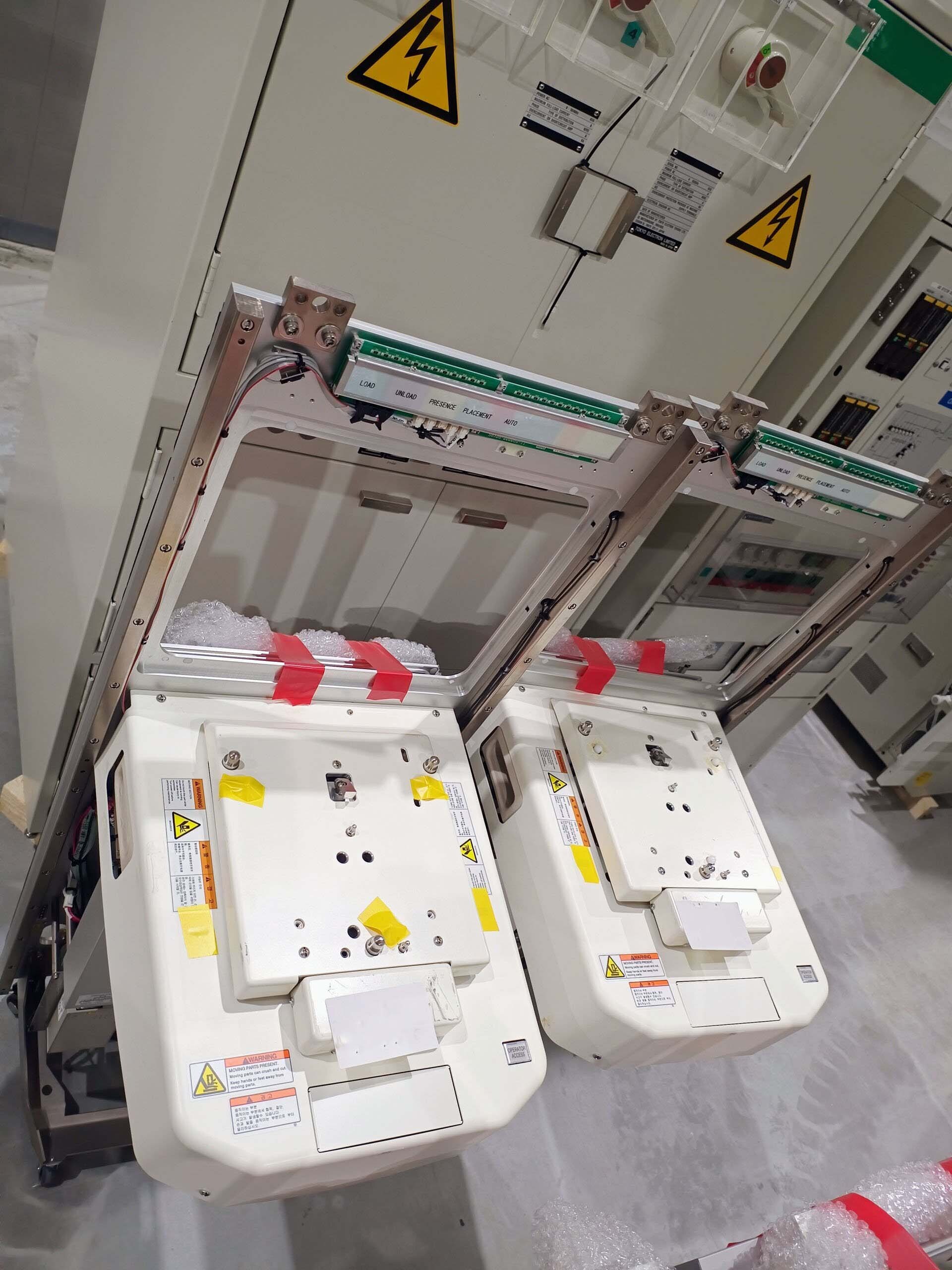
ID: 293770373
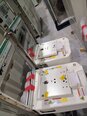
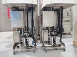
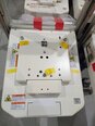
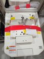
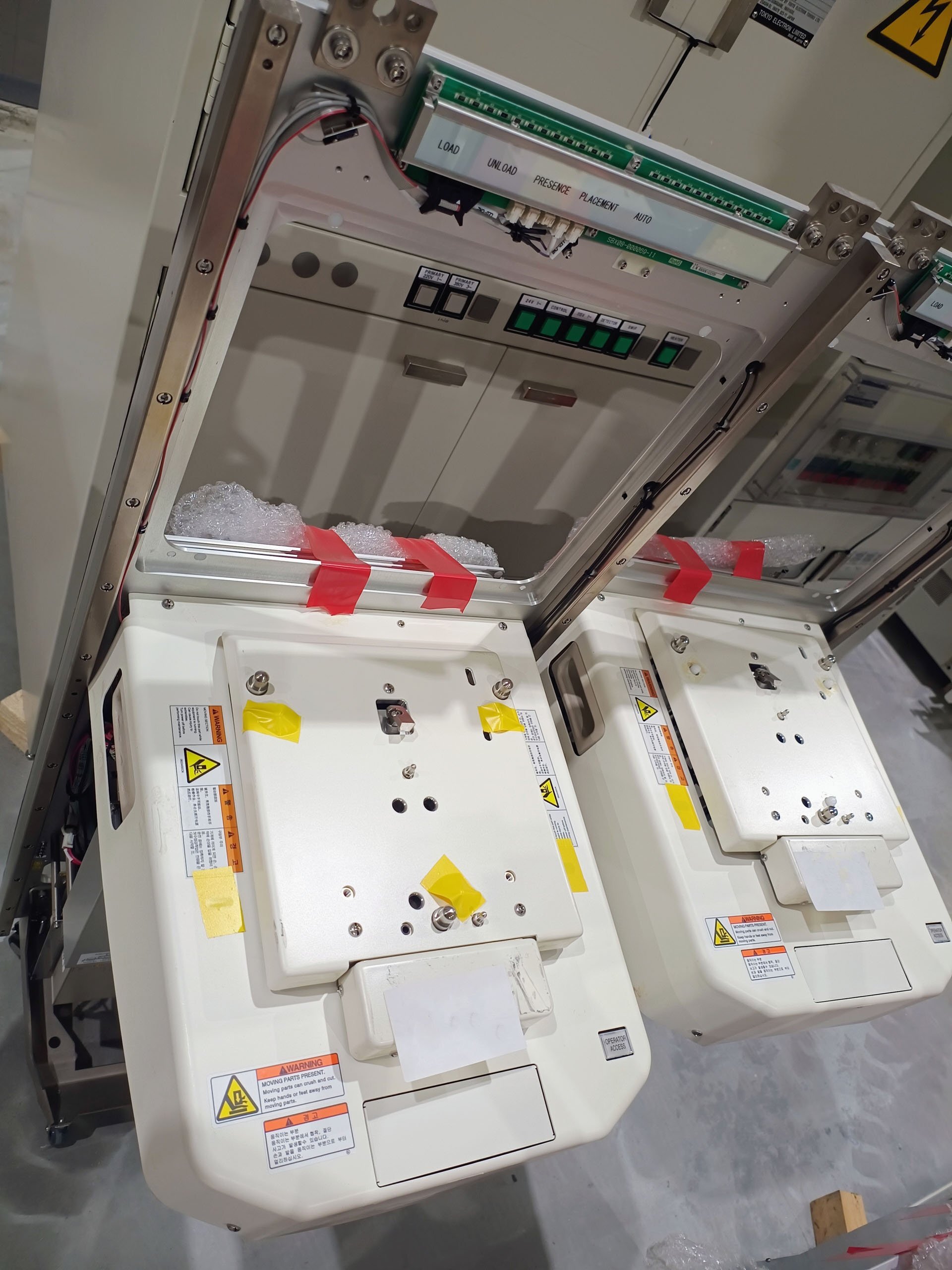
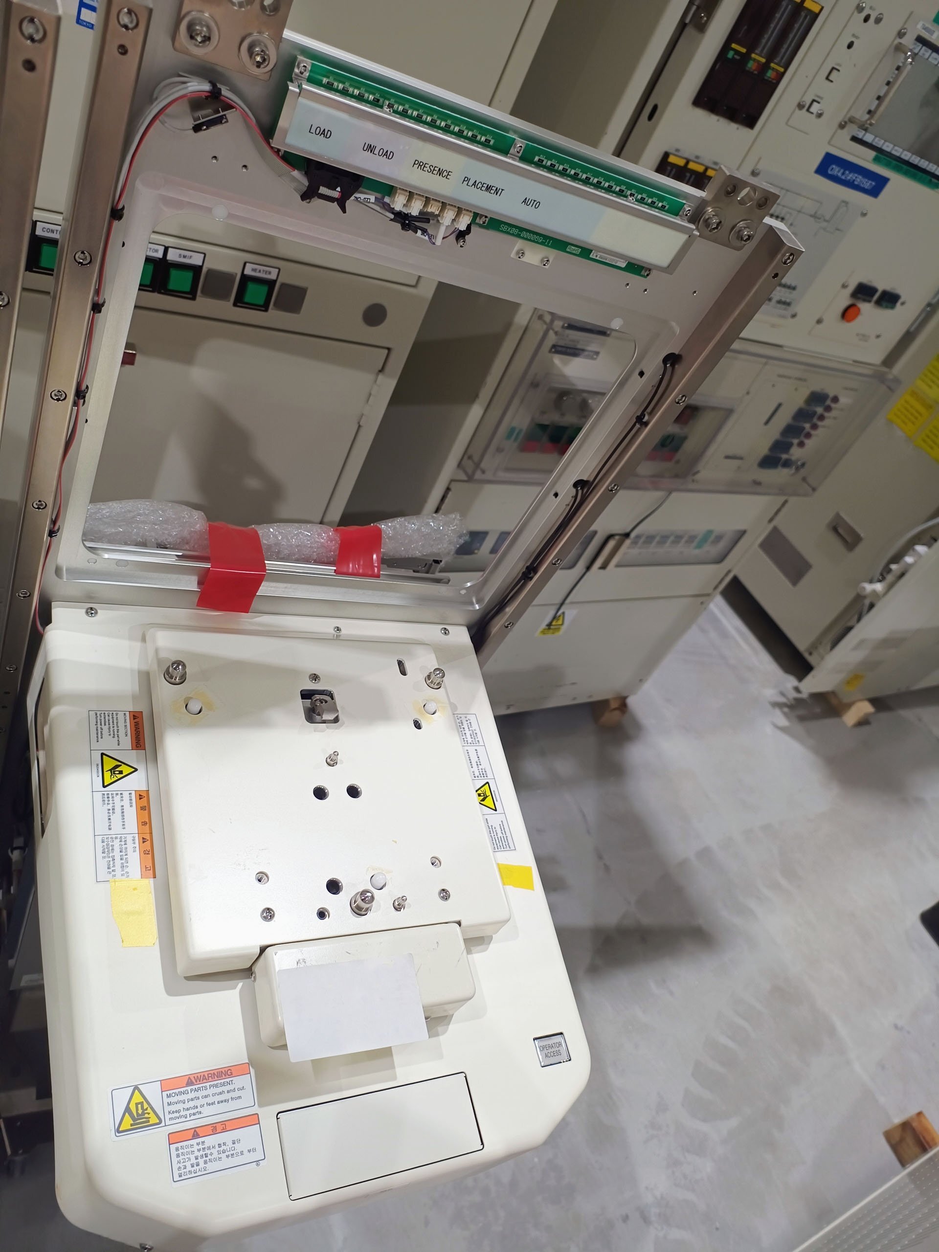
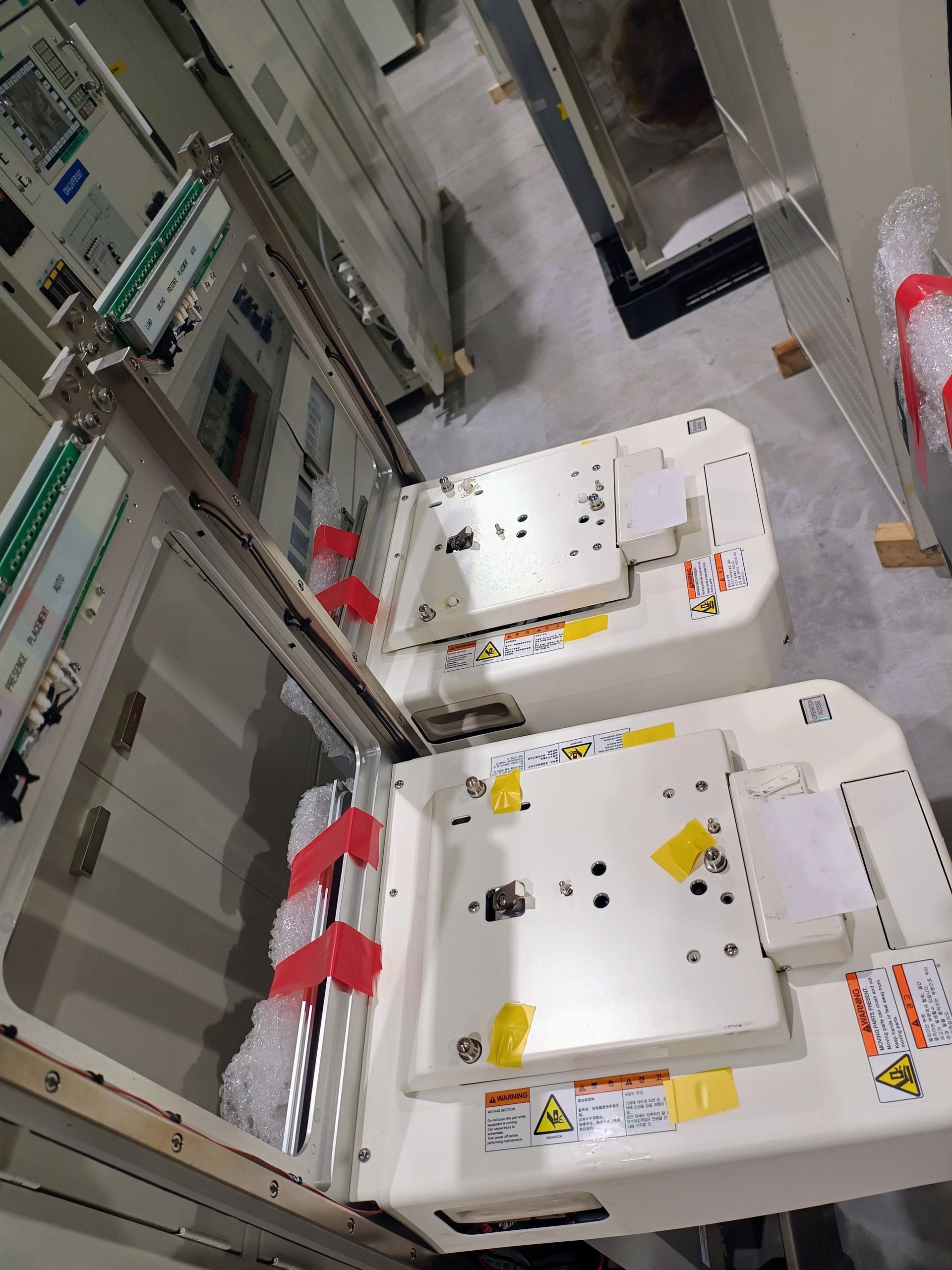
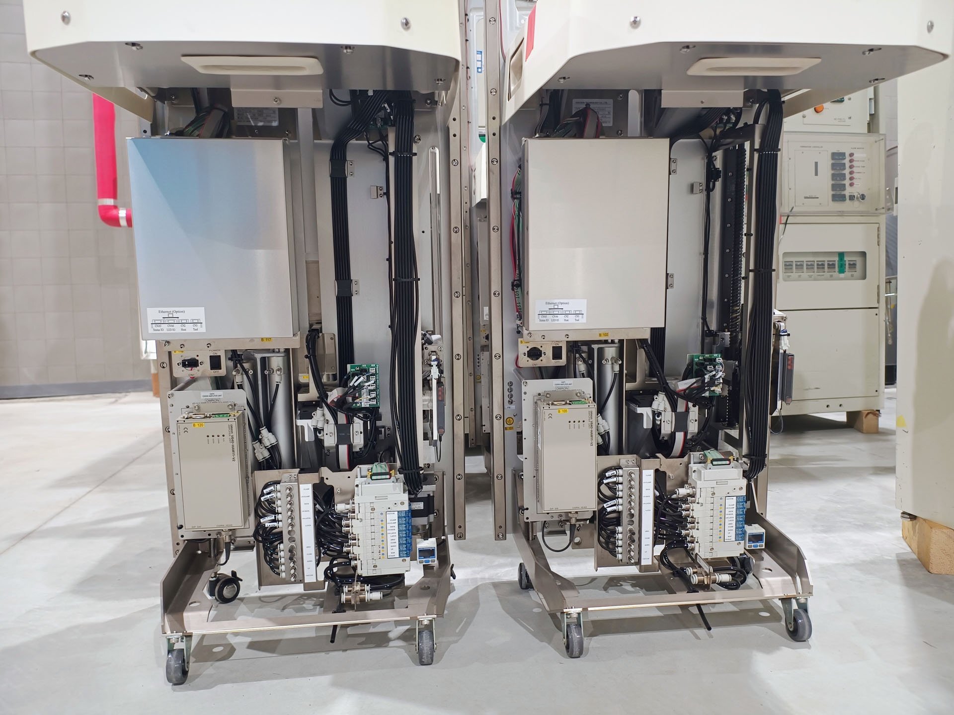
TEL / TOKYO ELECTRON equipment, also known as a photoresist TEL system, is a sophisticated and highly specialized piece of equipment used in the semiconductor industry for the fabrication of integrated circuits and other microelectronic devices. This TOKYO ELECTRON unit plays a crucial role in the photolithography process, which is a key step in semiconductor manufacturing that involves transferring a pattern onto a substrate using light.Machine consists of several key components that work together seamlessly to achieve precise and accurate patterning of photoresist material on semiconductor wafers. One of the primary components of TEL / TOKYO ELECTRON tool is the exposure tool, which is used to project a pattern onto the photoresist-coated wafer. This exposure tool typically utilizes a powerful light source, such as an ultraviolet laser, to generate the necessary light energy for the patterning process. In addition to the exposure tool, TEL asset also includes a variety of other components, such as a wafer handling TOKYO ELECTRON model, a wafer alignment equipment, and a photoresist coating/developing module. The wafer handling TEL / TOKYO ELECTRON system is responsible for precisely positioning and transferring the wafers within TEL unit, ensuring that the patterning process is carried out with the highest level of accuracy and consistency. The wafer alignment TOKYO ELECTRON machine is another critical component of tool, as it ensures that the pattern is aligned correctly with the underlying layers on the wafer. This alignment is crucial for achieving high-resolution patterning and reducing defects in the final semiconductor device. The photoresist coating/developing module is used to apply a uniform layer of photoresist material onto the wafer and then develop the exposed pattern after exposure. One of the key advantages of TEL / TOKYO ELECTRON asset is its ability to achieve high-resolution patterning with sub-micron accuracy. This level of precision is essential for the fabrication of advanced semiconductor devices with increasingly smaller feature sizes and higher levels of integration. TEL model is capable of patterning complex patterns with intricate geometries, enabling the production of cutting-edge microelectronic devices with improved performance and functionality. Moreover, TOKYO ELECTRON equipment offers excellent productivity and throughput, allowing semiconductor manufacturers to produce large volumes of devices quickly and efficiently. System is designed for high reliability and uptime, ensuring continuous operation and minimizing downtime in a semiconductor fabrication facility. Overall, TEL / TOKYO ELECTRON unit is a state-of-the-art solution for photolithography in the semiconductor industry, offering unparalleled precision, accuracy, and productivity for the fabrication of advanced microelectronic devices. Its advanced capabilities and sophisticated design make it an indispensable tool for semiconductor manufacturers seeking to push the boundaries of technology and innovation in today's competitive marketplace.
There are no reviews yet