Used TEL / TOKYO ELECTRON ZETA #293816249 for sale
URL successfully copied!
Tap to zoom
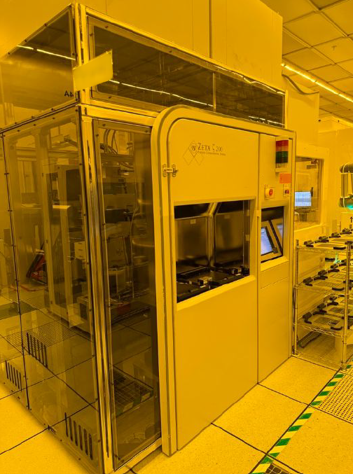

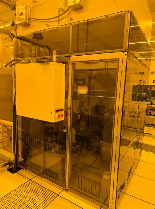

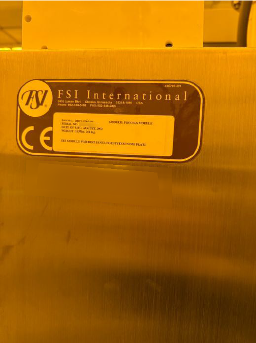
ID: 293816249
Wafer Size: 8"
Vintage: 2002
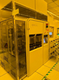
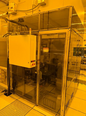
System, 8"
(2) Standard Mechanical Interface (SMIF) pods
Staubli Robot
2002 vintage.
TEL / TOKYO ELECTRON ZETA is a cutting-edge photoresist equipment developed by TEL Limited (TOKYO ELECTRON), a leading semiconductor equipment manufacturer. This innovative system is designed to meet the evolving demands of the semiconductor industry by providing advanced capabilities for photolithography processes critical in the fabrication of semiconductor devices. TEL ZETA photoresist unit features a highly efficient and precise exposure mechanism that enables superior patterning control at submicron levels. The machine utilizes advanced optics and illumination sources to project intricate patterns onto a photoresist-coated substrate with exceptional accuracy and uniformity. This level of precision is essential for defining the intricate structures and circuit patterns that make up the integrated circuits essential to modern electronic devices. One of the key strengths of TOKYO ELECTRON ZETA tool is its versatility and adaptability to a wide range of photoresist materials and formulations. The asset is capable of handling various types of photoresists, including positive and negative resist formulations, as well as specialized materials such as chemically amplified resists. This flexibility allows semiconductor manufacturers to choose the most suitable photoresist for their specific process requirements, including sensitivity, resolution, and etch resistance. In addition to its advanced exposure capabilities, ZETA model incorporates state-of-the-art alignment and registration technologies to ensure the accurate overlay of multiple lithographic layers. This is crucial for achieving the tight dimensional tolerances required for advanced semiconductor designs and maintaining the integrity of the device's functionality. Furthermore, TEL / TOKYO ELECTRON ZETA equipment offers enhanced process control features that enable real-time monitoring and optimization of critical process parameters. These capabilities help ensure consistent and repeatable patterning results, ultimately leading to higher yields and improved device performance. The system is also equipped with advanced automation and robotics capabilities to streamline the lithography process and maximize throughput. This high degree of automation reduces the risk of human error, increases productivity, and enables semiconductor manufacturers to meet the demanding production schedules of the semiconductor industry. Moreover, TEL ZETA unit features a user-friendly interface and intuitive software that facilitate ease of operation and efficient process setup. This allows operators to quickly program and execute complex lithography processes, as well as analyze and troubleshoot any issues that may arise during production. Overall, TOKYO ELECTRON ZETA photoresist machine represents a significant advancement in lithography technology, offering semiconductor manufacturers the precision, flexibility, and control required to produce the next generation of high-performance semiconductor devices. With its state-of-the-art capabilities and advanced features, this tool is poised to play a crucial role in shaping the future of the semiconductor industry and driving innovation in electronic devices.
There are no reviews yet