Used VON ARDENNE WM70H / C #9172921 for sale
URL successfully copied!
Tap to zoom






















ID: 9172921
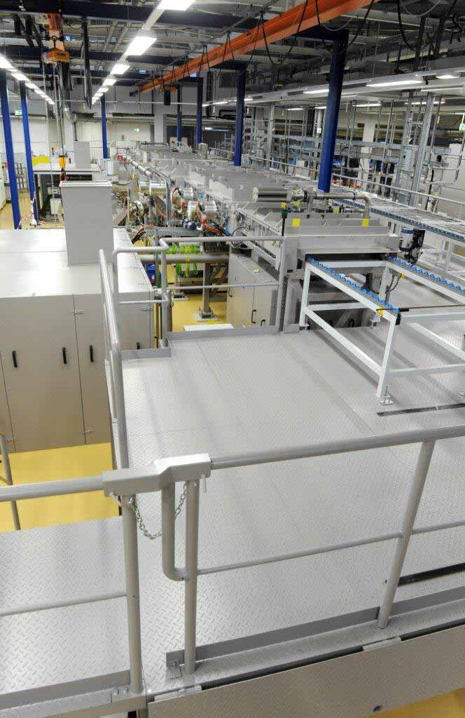
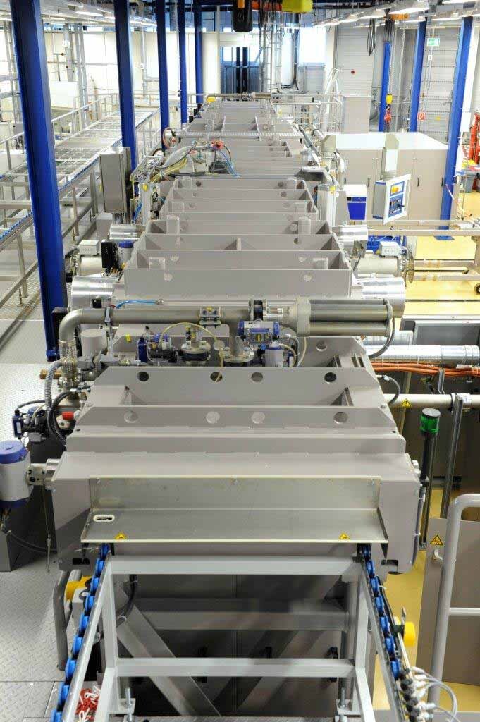
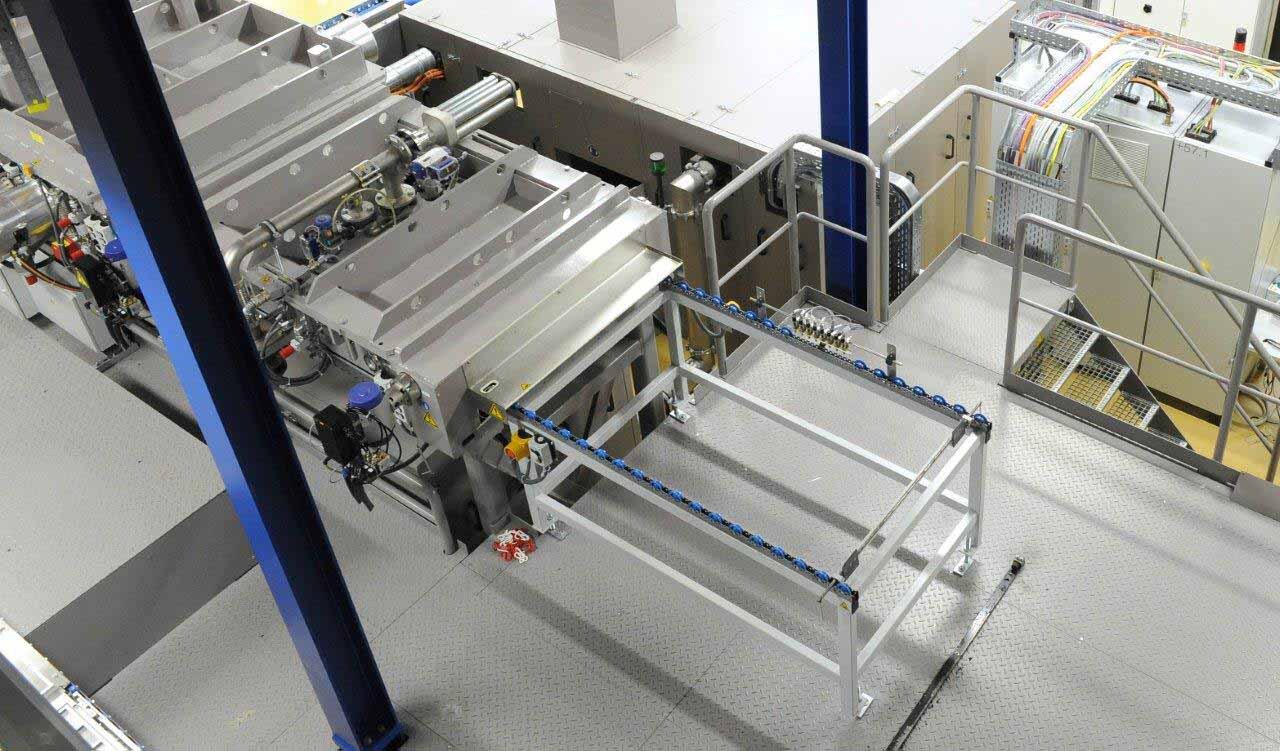
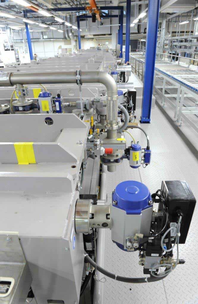
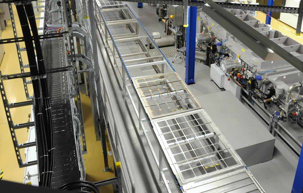
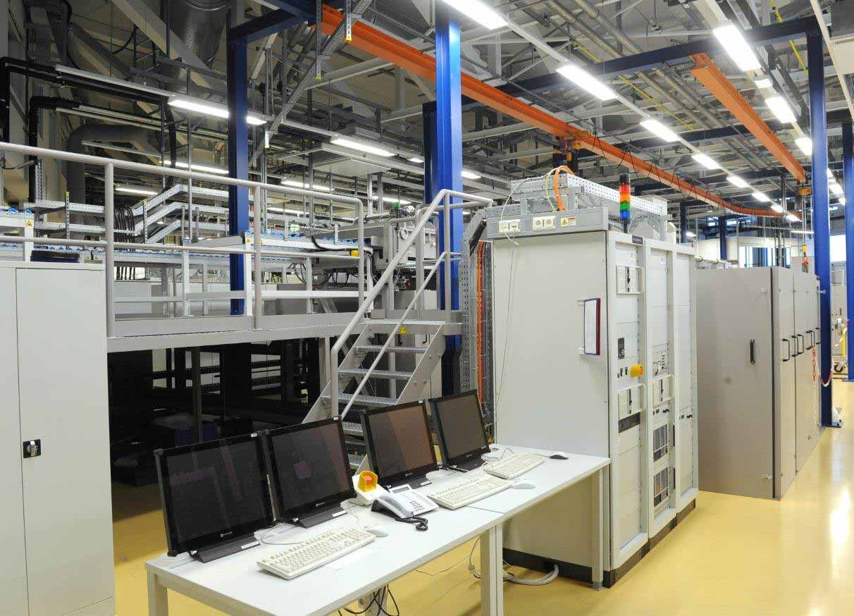
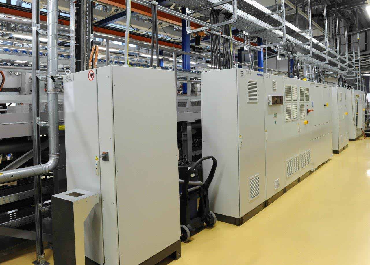
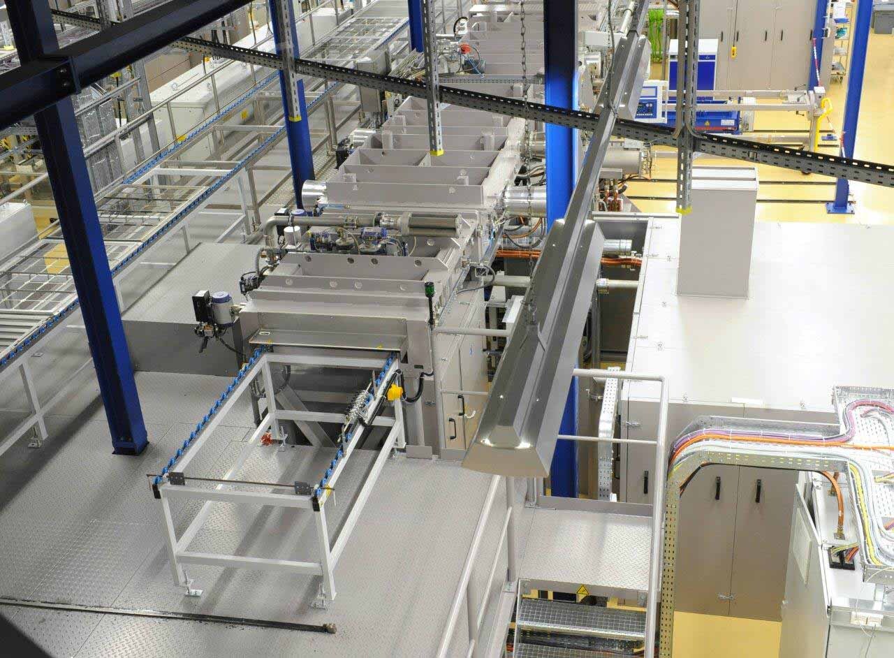
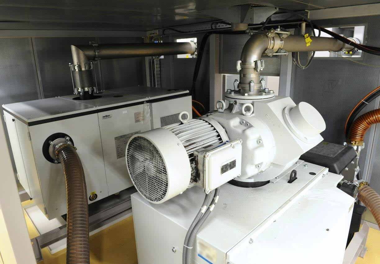
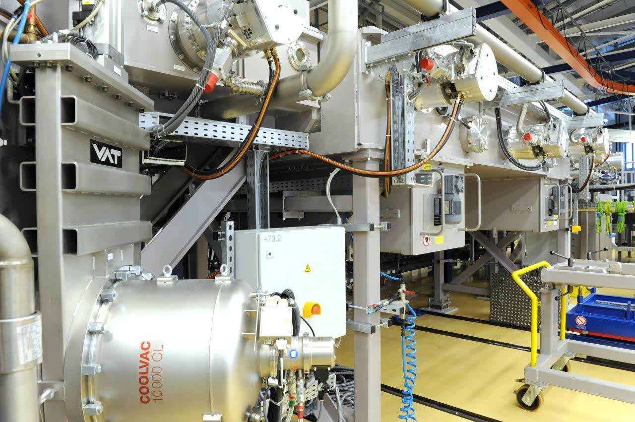
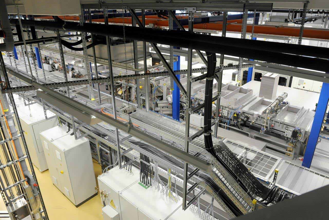
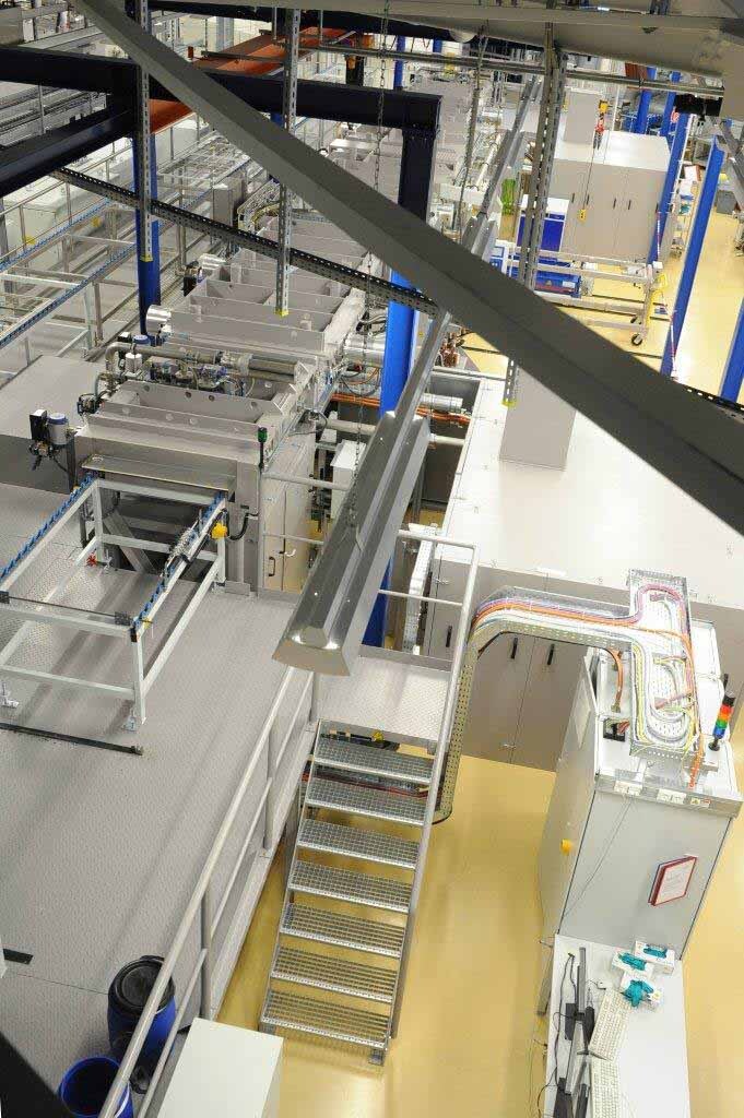
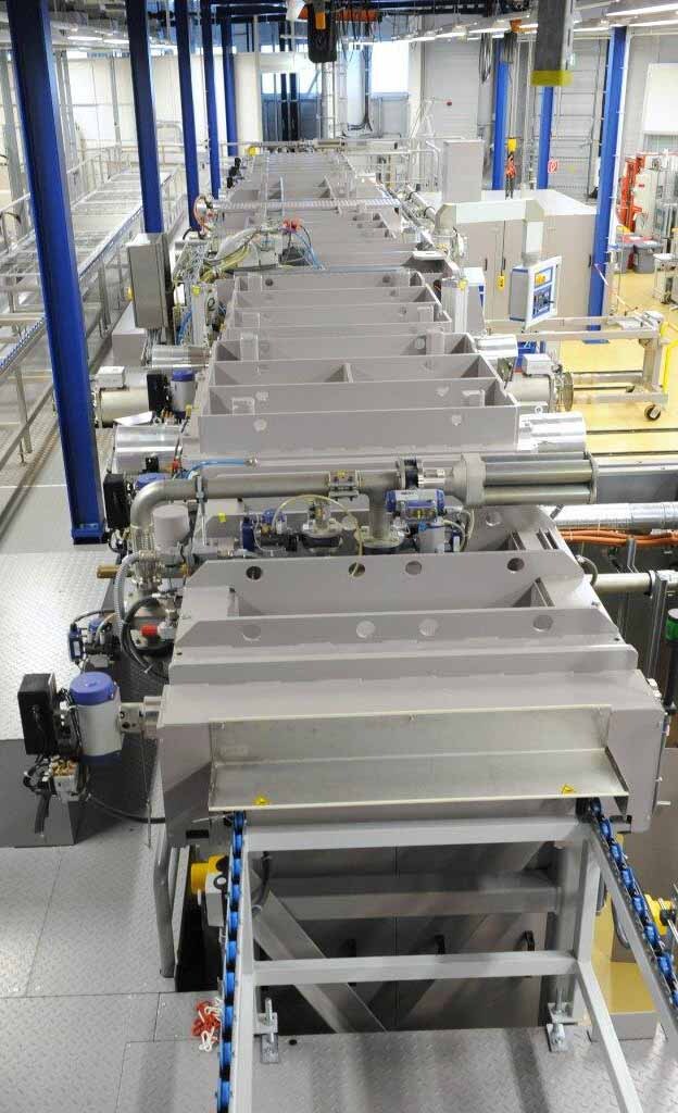
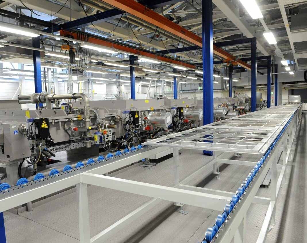
High end coating line
Wafer metallizer
In-line complete system for coating wafers
Back coating of silicon wafers with an aluminum layer
Coating of nickel, silver and aluminum by electron beam evaporation
(35) Cells can be coated per tray
Productivity:
4,000 Wafers (5") per hour
2,600 Wafers (6") per hour
Cycle time: 50s
Technical parameters:
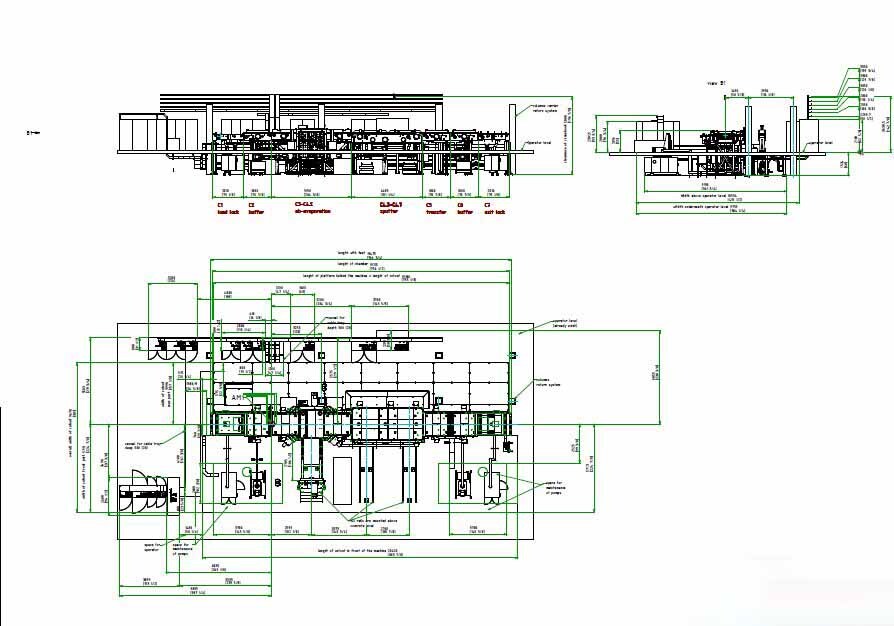
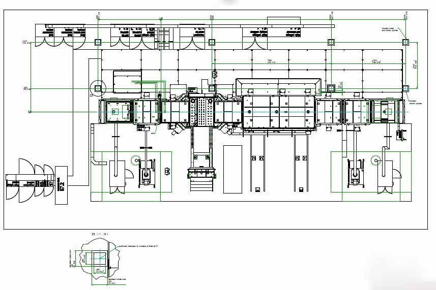
System dimensions:
Length: 19 m
Area: 20 x 7 m
Height: ~3 m
Drive:
Carrier speed max: 5 m/min
Carrier speed during vapor deposition: 1.5 - 2.0 m/min
Substrate temperature:
Max. temperature: 300°C / 572°F
Carrier dimensions:
Length: ~1,450 mm
Width: 925 mm
(60) Wafers (5") per carrier
(40) Wafers (6") per carrier
Ambient conditions:
Ambient temperature:
+15 to 35 °C
+59 to 95 °F
Relative humidity at 30°C / 86°F: < 70 %
Dust: < 10 mg/m3
Sluice chambers C1 and C7
Buffer chambers C2 and C6
Transfer chamber C5
Process chamber C4:
EB Chamber C3 / C4.1 / C4.2
Sputter chambers
(5) Sections (C4.3 to C4.7)
Vacuum
Working pressure:
C2 - Buffer chamber 2 to 5 x 10⁻³ mbar
C4.1 - EB chamber 5 to 9 x 10⁻⁵ mbar
C4.2 - Intermediate chamber 2 to 5 x 10⁻⁴ mbar
C4.3 - Intermediate chamber 2 to 5 x 10⁻³ mbar
C4.4 - Sputter chamber 2 to 5 x 10⁻³ mbar
C4.5 - Pump chamber 2 to 5 x 10⁻³ mbar
C4.6 - Sputter chamber 2 to 5 x 10⁻³ mbar
C4.7 - Intermediate chamber 2 to 5 x 10⁻³ mbar
C5 - Transfer chamber 2 to 5 x 10⁻³ mbar
C6 - Buffer chamber 2 to 5 x 10⁻³ mbar
Leak rate: < 1 x 10⁻² mbar l/s-1
Layer thickness / Properties:
AI with copper:
Thickness: 2 μm
Wafer thickness: > 200 μm
Temperature: 400°C / 752°F
Purity: 99.98%
AI with ceramic:
Thickness: 3 μm
Wafer thickness: 150 to 250 μm
Temperature: 300°C / 572°F
Purity: 99.5%
Ag: Thickness: < 300 nm
Sn: Thickness: < 300 nm
NiCr: Thickness: < 40 nm
Uniformity: ± 10%
Evaporation:
Production cycle: 120 h
Power of electron beam
Copper crucible: 100 to 200 kW
Ceramic crucible: 20 kW
Target material per cycle: 90 to 150 kg
Vapor utilization: 48 to 50 %
Target-substrate distance: 600 mm
Carrier frequency: 60s
Sputtering:
Target material: Ag
Target utilization: ~70%
Target life: 240 h
Cooling water:
Particle size: ~50 mg/l
pH Value: (8.0 to 9.0)
Electrical conductivity: (150 to 250) μS/cm
Acid capacity, Ks 4.3: (0.5 to 2.0) mmol/l
Filterable substances: < 50 mg/l
Chloride: < 10 mg/l
Sulfate: < 30 mg/l
Ammonium: < 0.5 mg/l
Nitrate: < 10 mg/l
Colony count (CFU): ~ 1,000 ml-1
TOC (total organic carbon): < 1.5 mg/l
Inlet temperature:
21 to 25°C
69.8 to 77°F
Differential pressure: 2 bar
Absolute pressure max: 8 bar
Water circuit 1 chambers:
Volume flow: TBD m3/h
Temperature: 25°C / 77°F
Required pressure: 6 - 8 bar
Cooling capacity: TBD kW
Electrical system:
3 Phases, 3 AC 480 V
Tolerance: -10/+6 %
Frequency: 59 to 61 Hz
Grounding resistance: <2 Ohm
Connected load max: 400 kVA
Function:
Wafers are coated on one side with (2) metal layers.
VON ARDENNE WM70H / C is an advanced Photoresist equipment capable of producing high-quality thin-film images and patterns. The system is designed to create sizes down to 70 nm in width and 100 nm in height with an accuracy of 2 nm. The unit comprises of several components such as photomasks, a lithography machine, numerous fluidic components, a gas dispenser, and a resist source. The photomasks, which are used to pattern the wafer's surface, are first loaded into the lithography machine. Then, the fluidic components rapidly dispense the resist (a chemical mixture) onto the photomask and the wafer and help to spread it uniformly. The resist is then exposed to light from a flood source to create a resist pattern that functions as a template into which the surface details will be formed. A gas dispenser precisely applies a protective fluorocarbon film over the resist surface to handle the gas flow and insure emulsion consistency. The resist is then stripped, rinsed, and dried, and the wafer is then ready to undergo a further etching process and for the resist to be stripped. TheWM70H/C machine features the most cutting-edge components in the market and provides a superior image placement accuracy, precision pattern definition, and high-fidelity film structuring for semiconductor lithography processes between 70-100 nm. When used in combination with a post-etch harmonic imaging tool, WM70H / C provides clear, detailed features, with an accuracy of 2 nm. Furthermore, its wide range of parameters and automated operations guarantee minimal setup time, which results in significant productivity gains. It is ideal for high-volume production environments of advanced semiconductor processes.
There are no reviews yet


