Used ZEISS A20 #293770641 for sale
URL successfully copied!

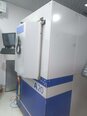
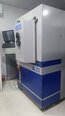
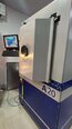
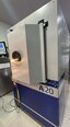
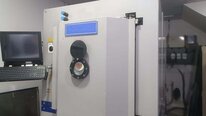
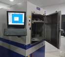
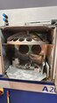



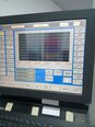




























Tap to zoom
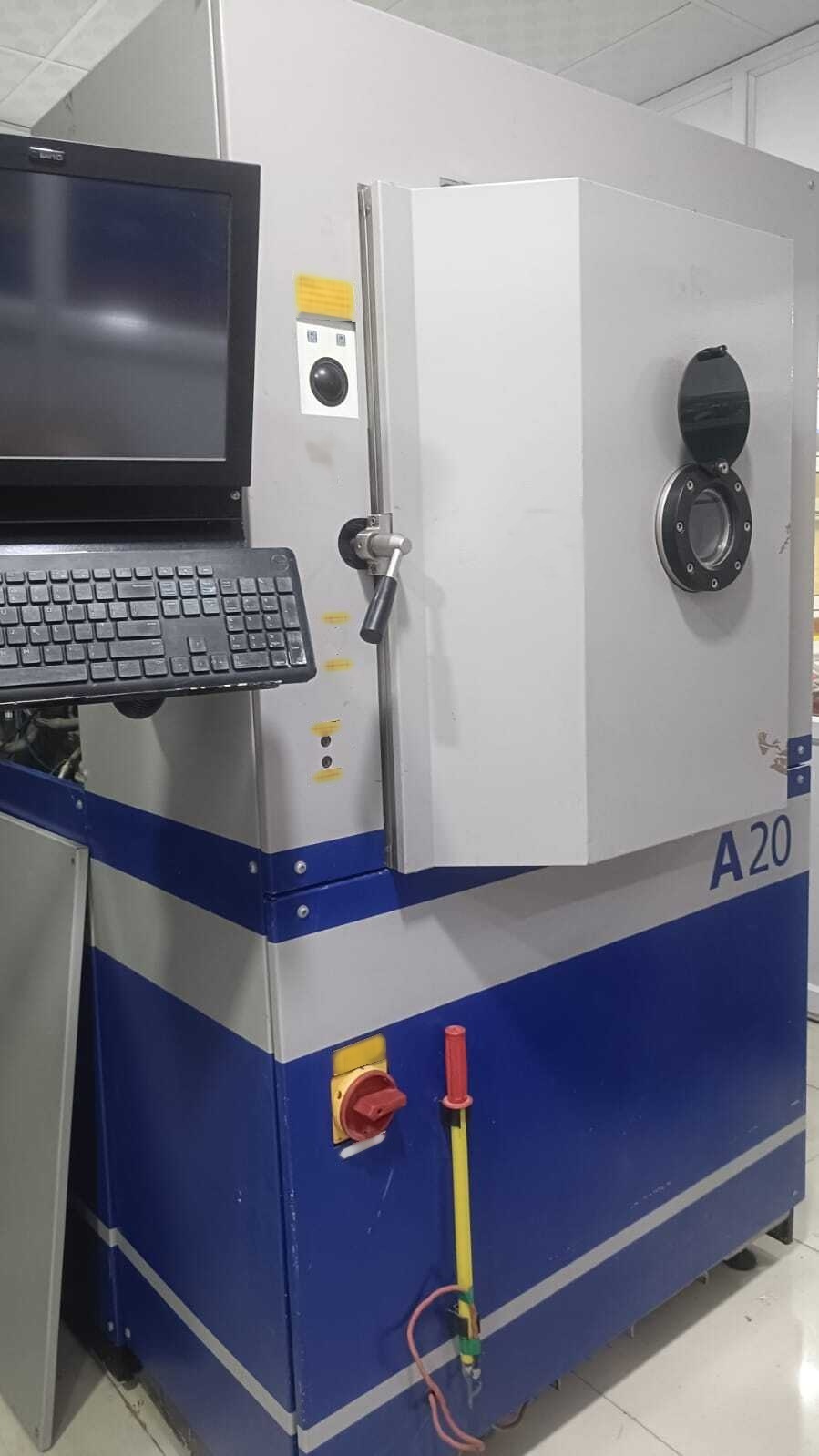

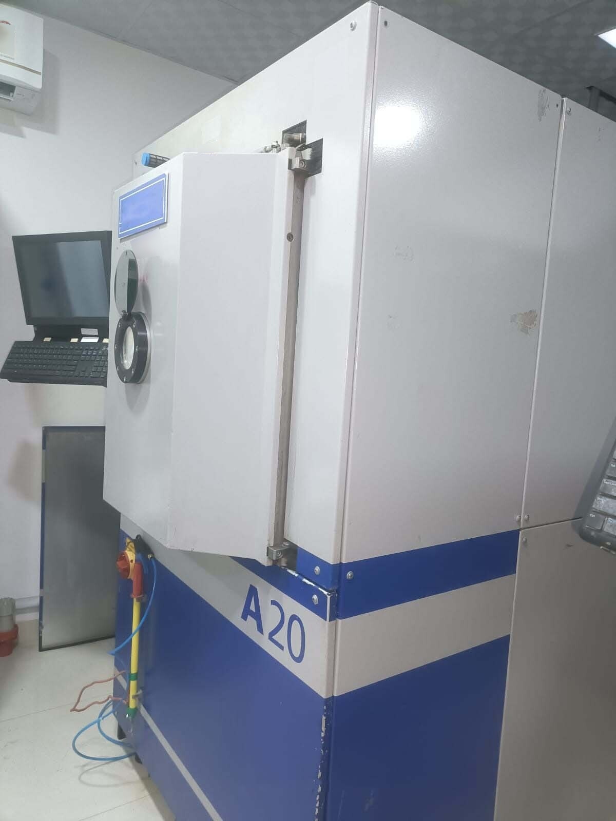
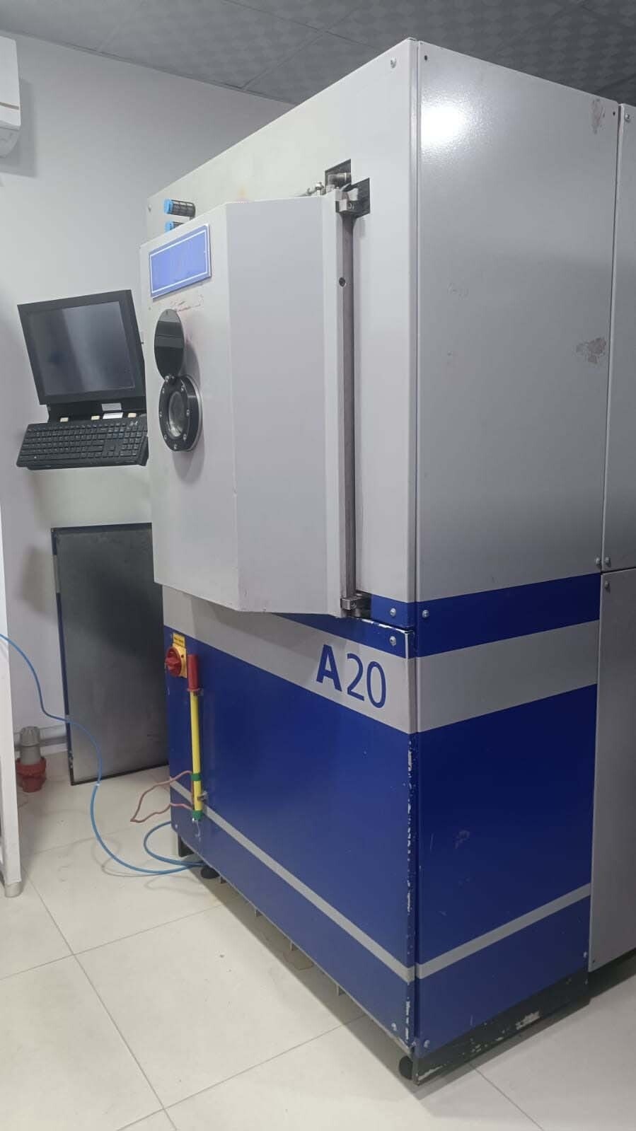
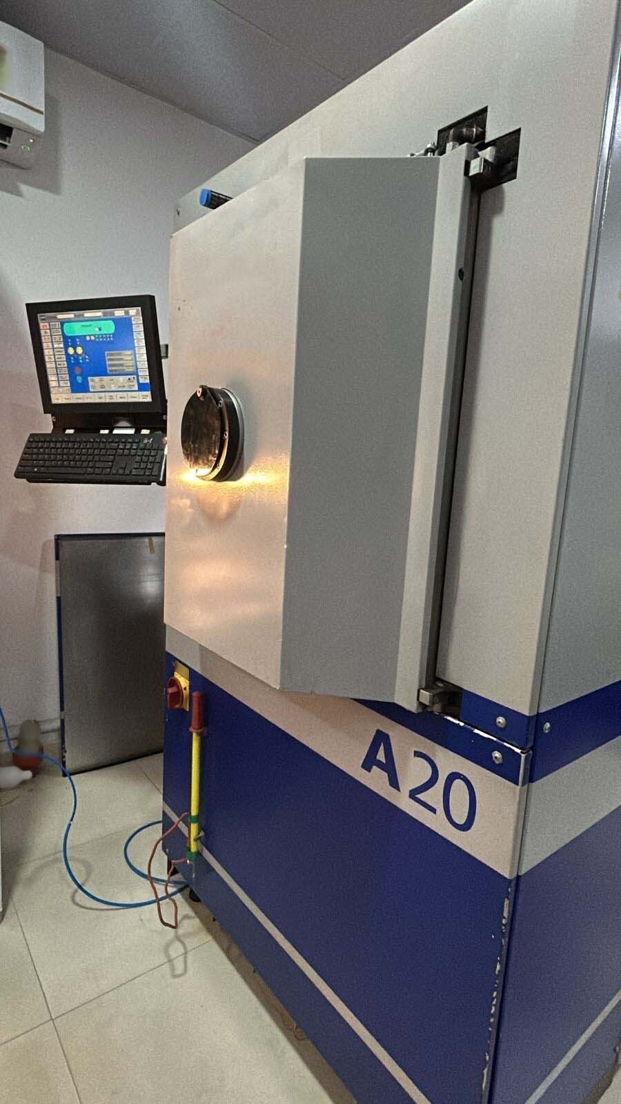
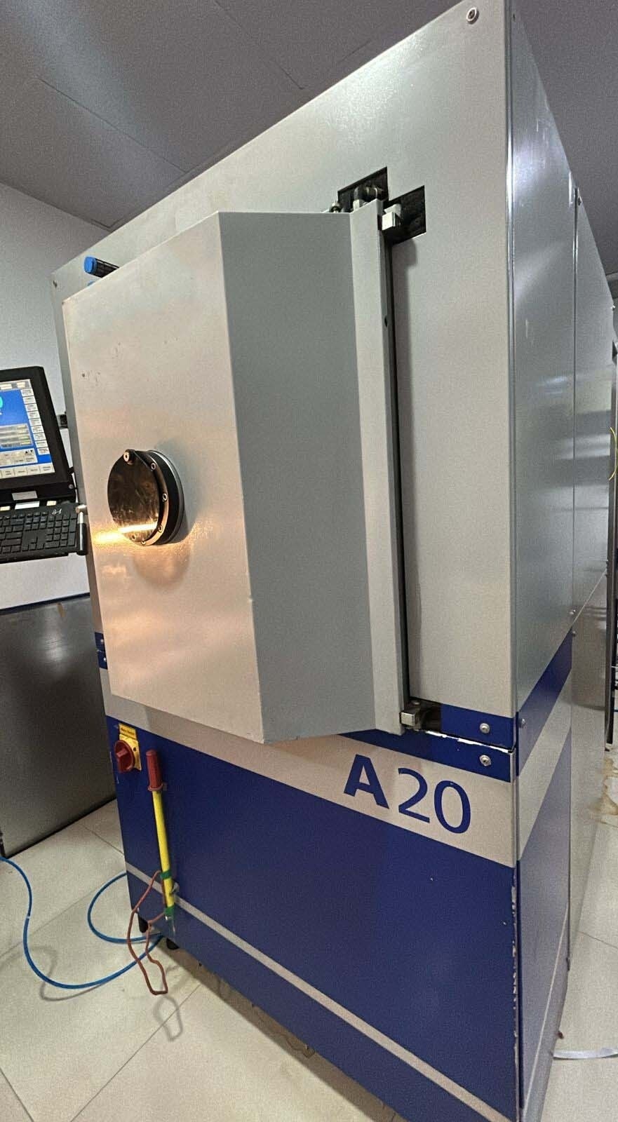
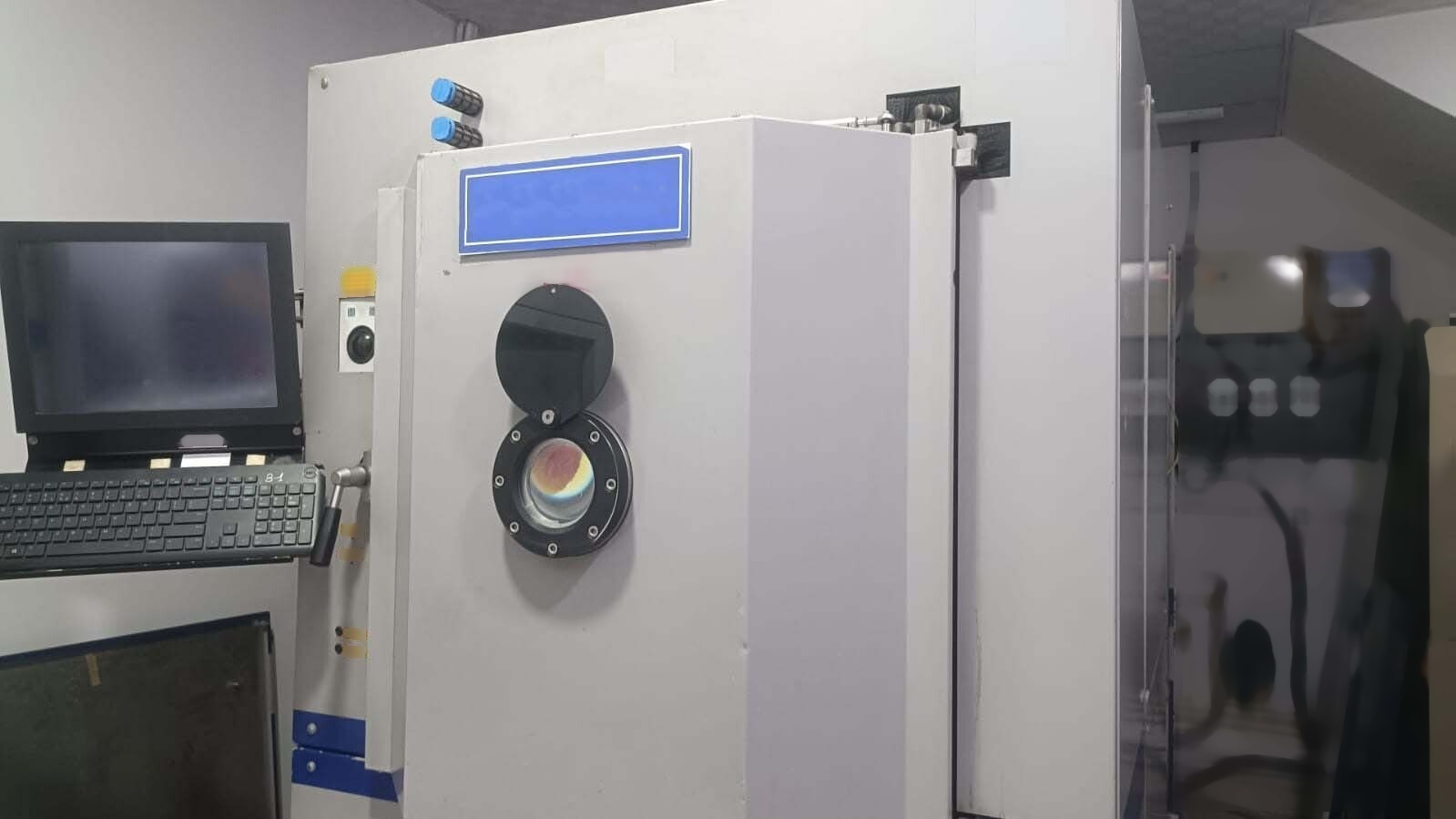
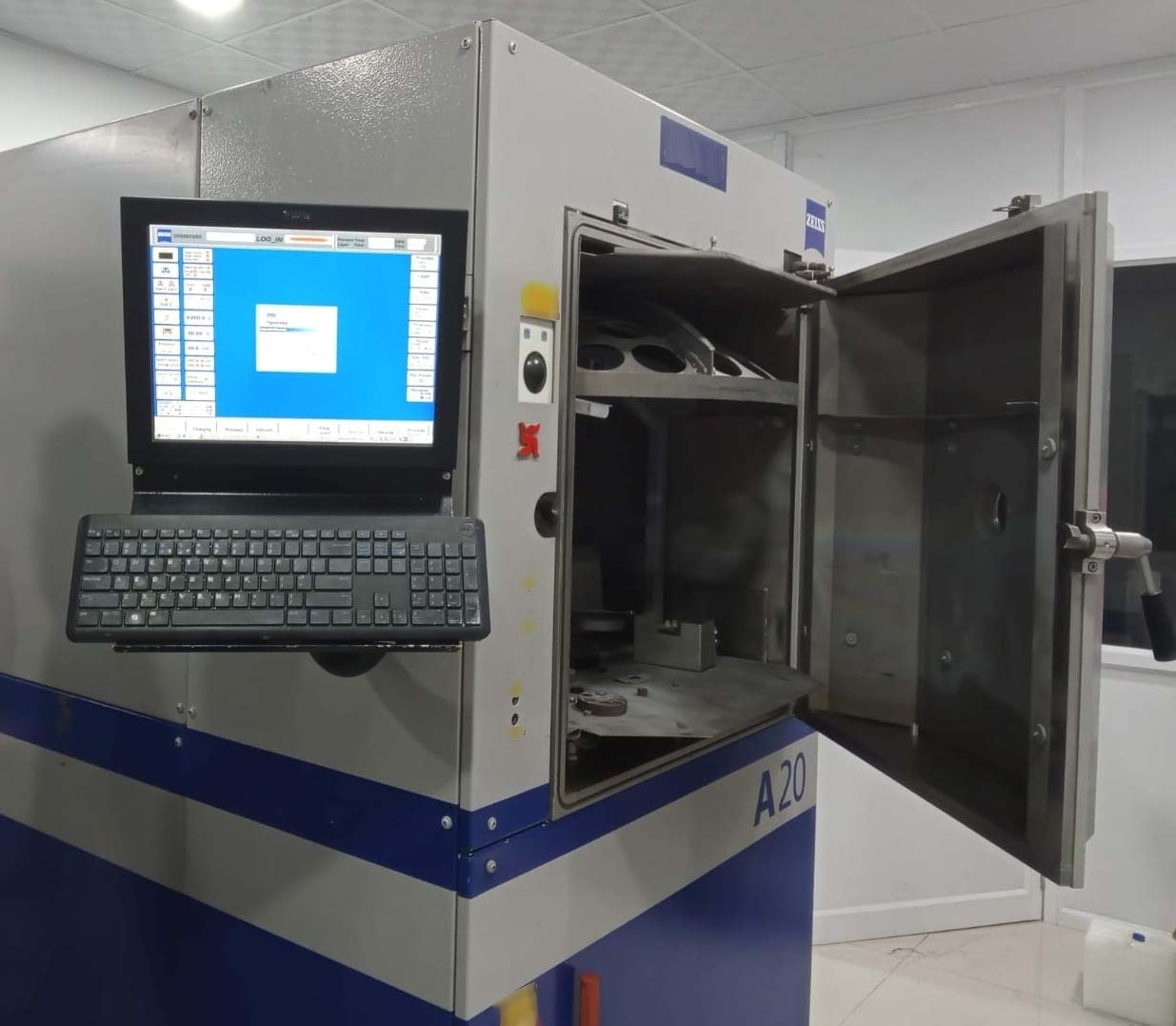
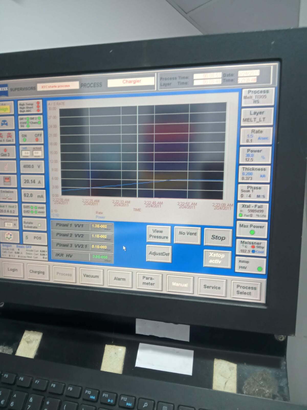
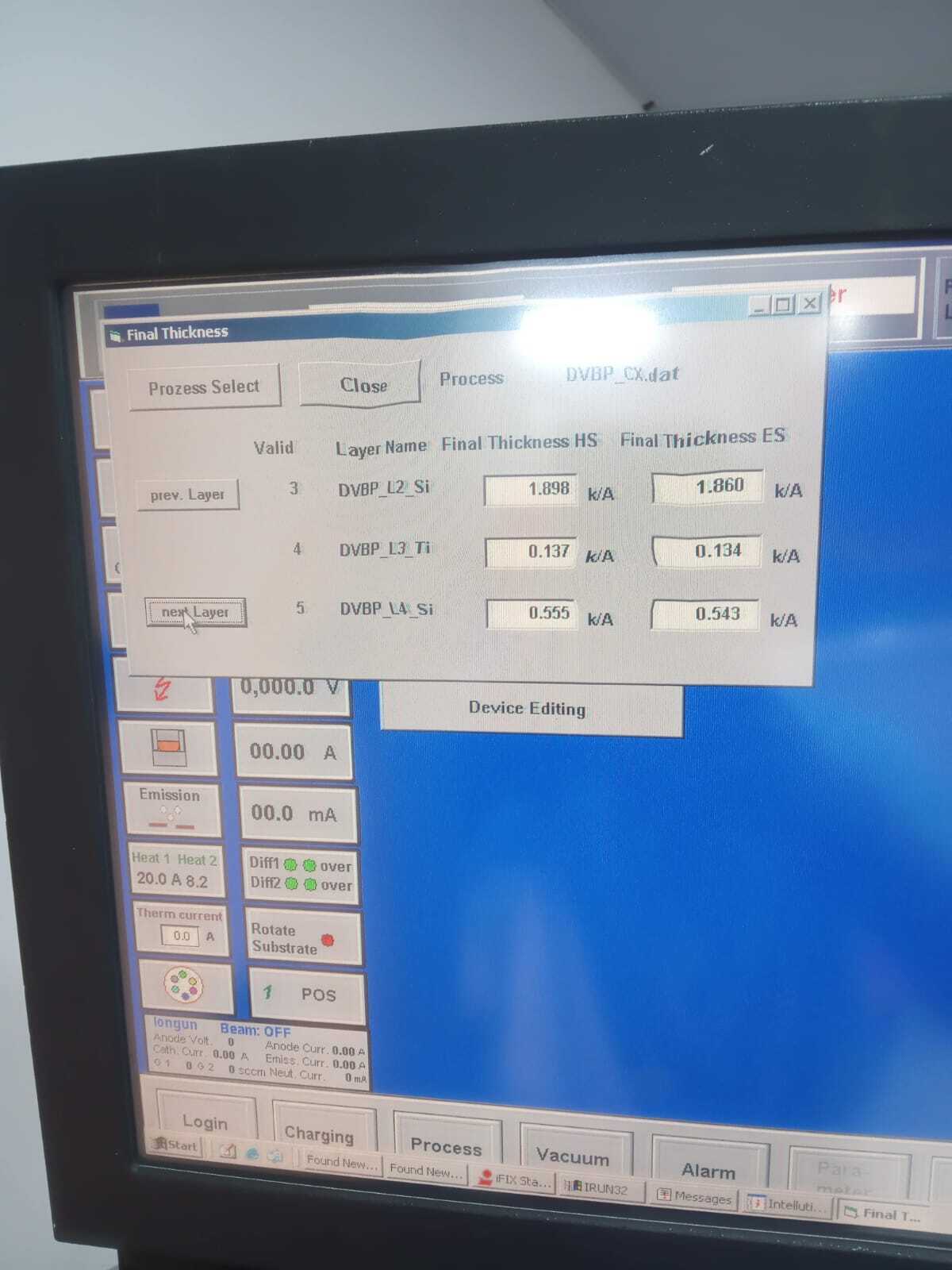
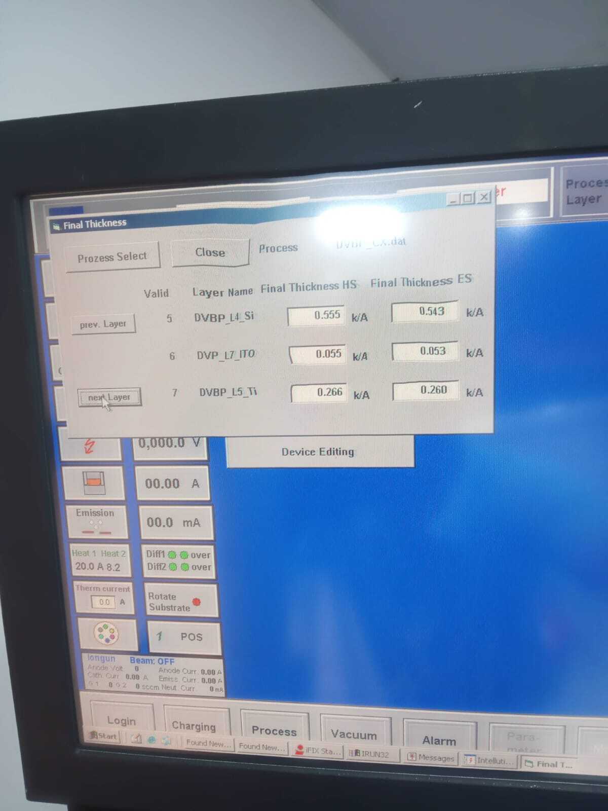
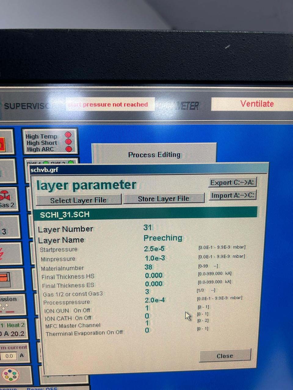
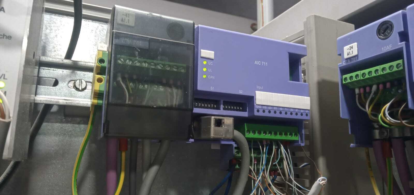
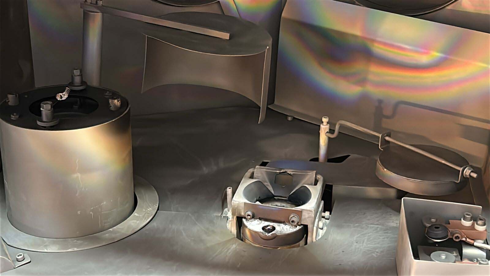
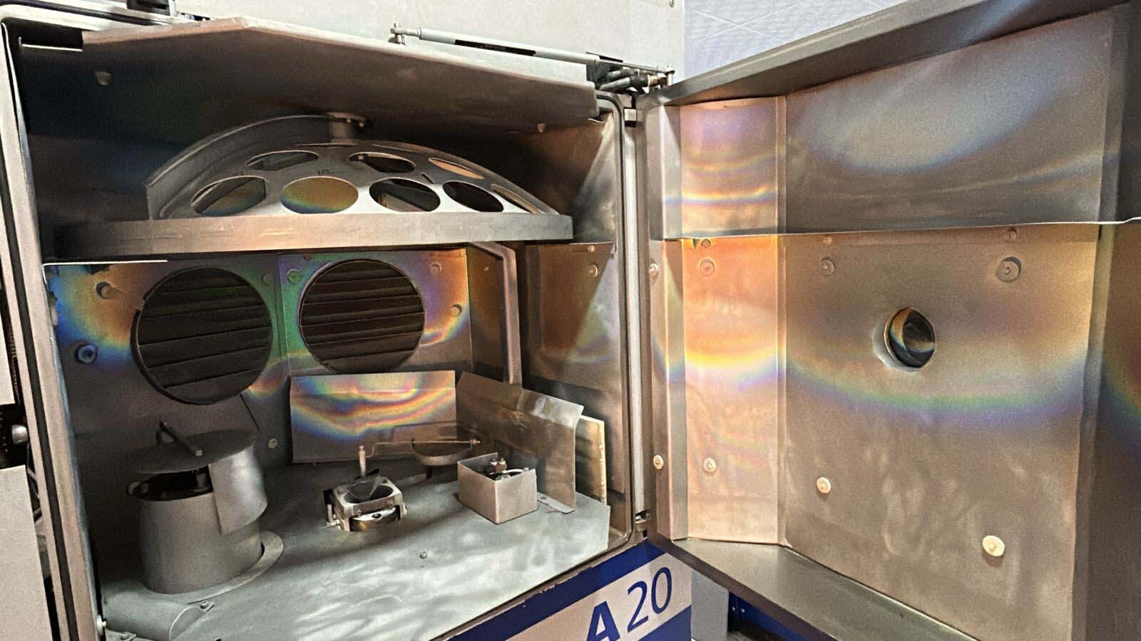
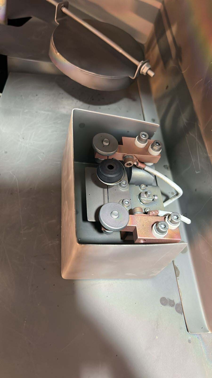
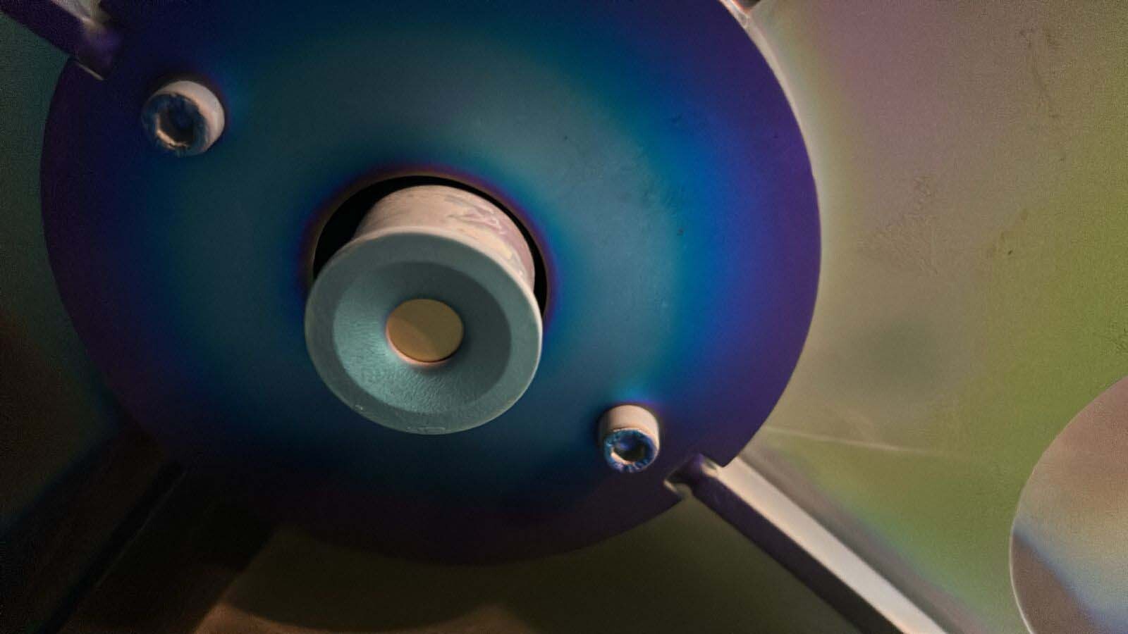
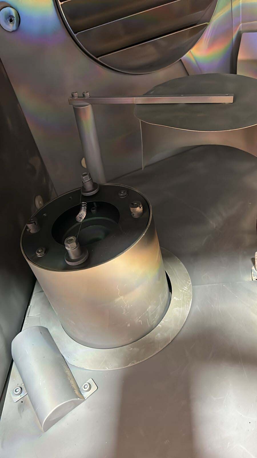
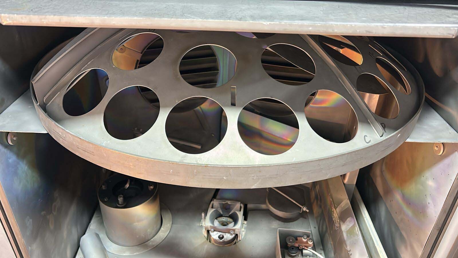
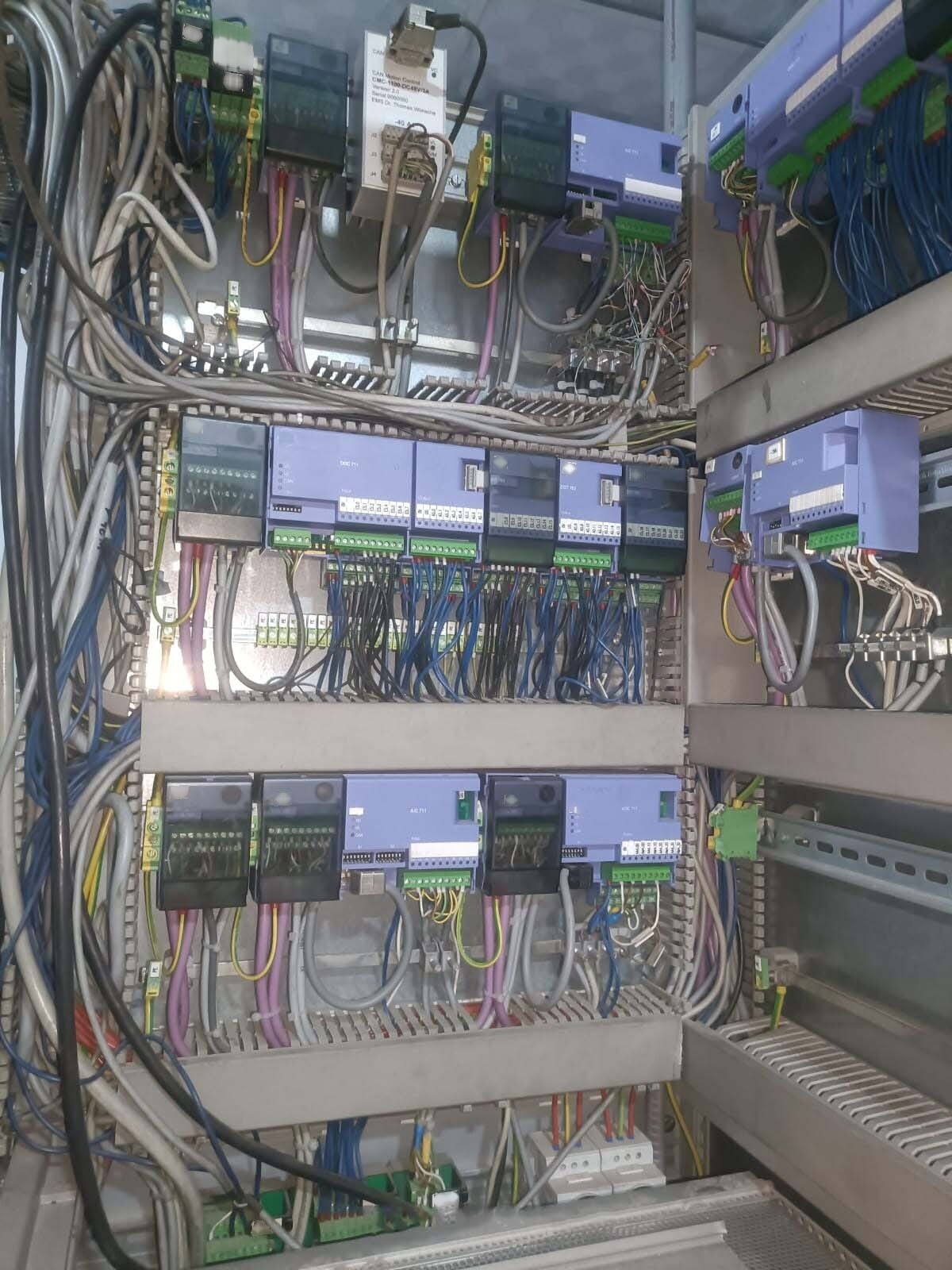
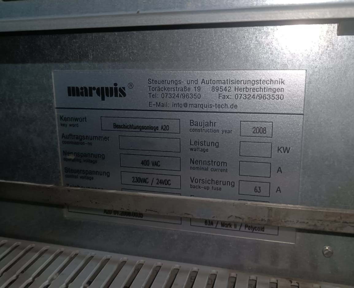
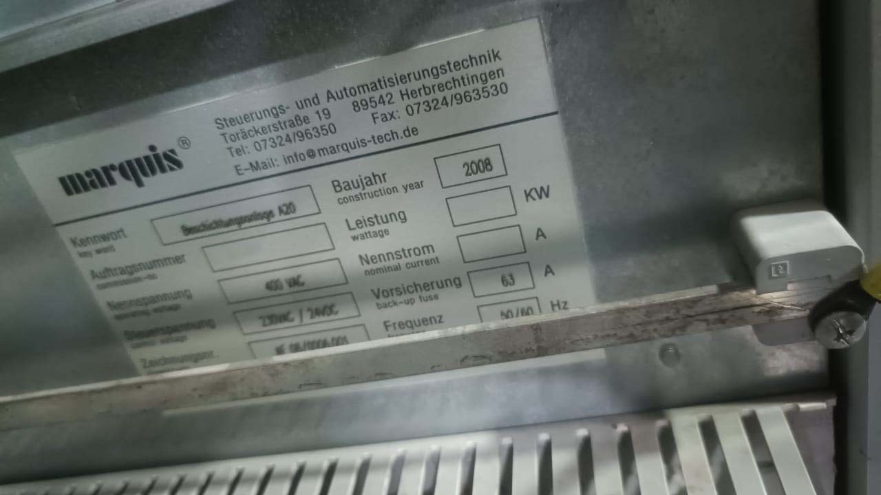
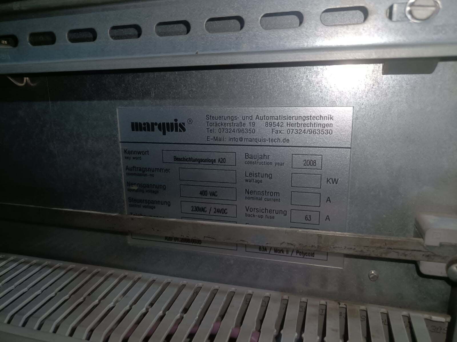
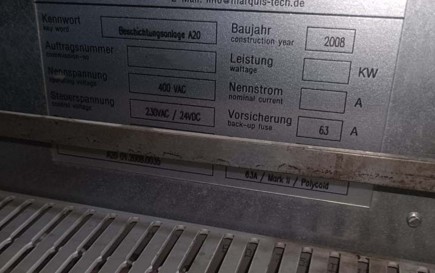
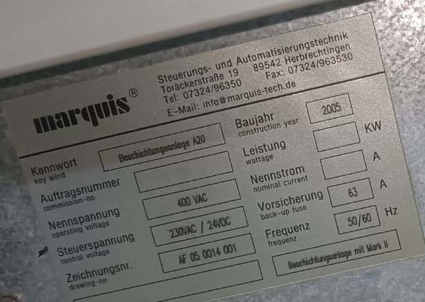
ID: 293770641
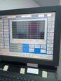
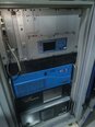
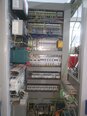
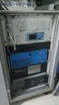
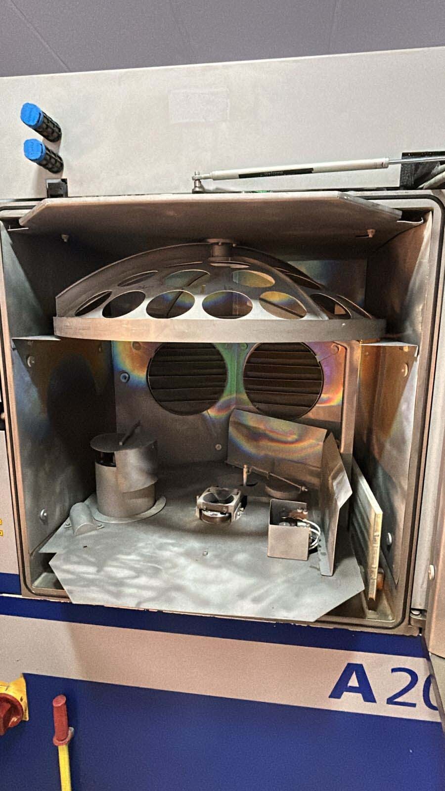
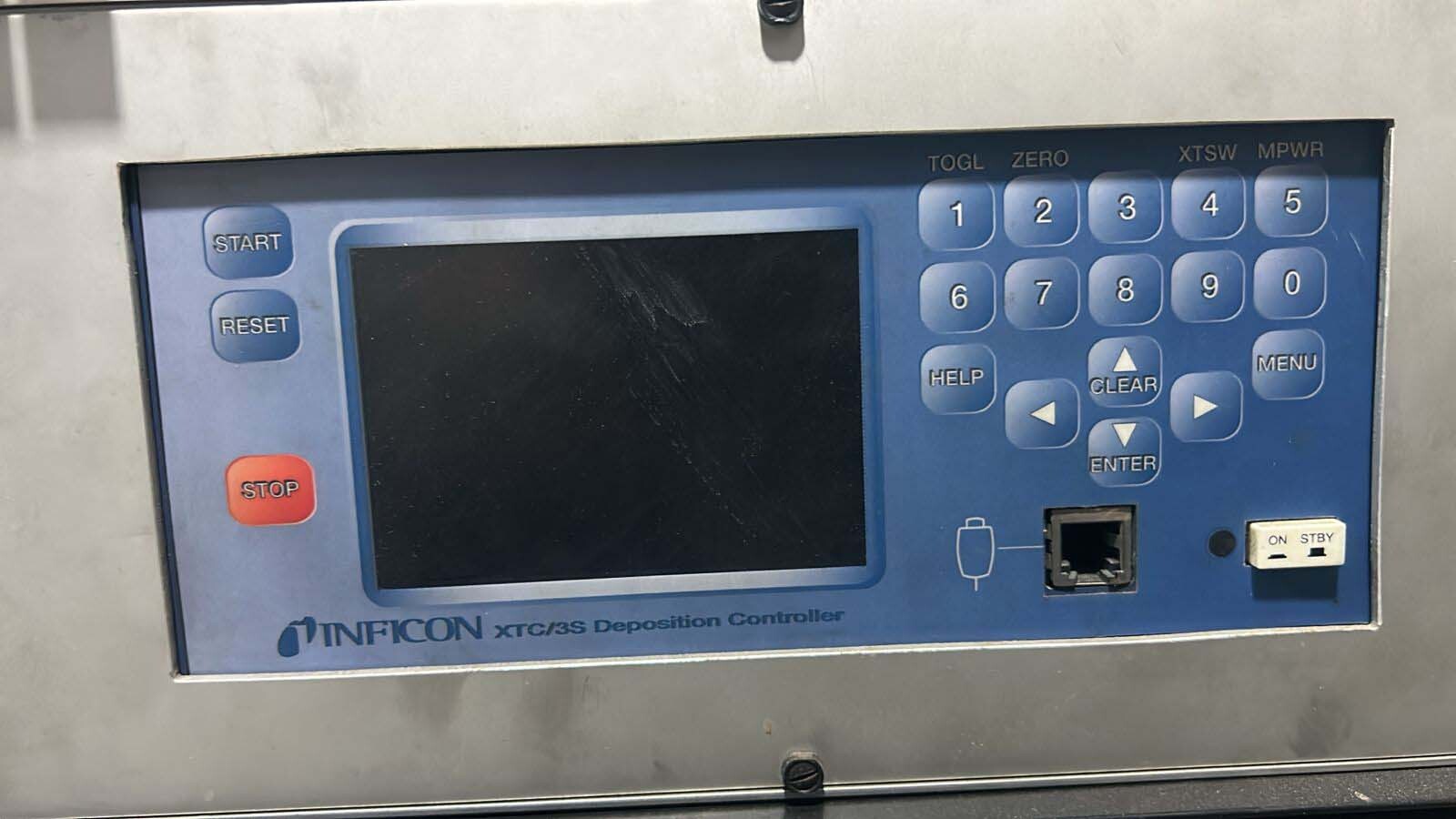
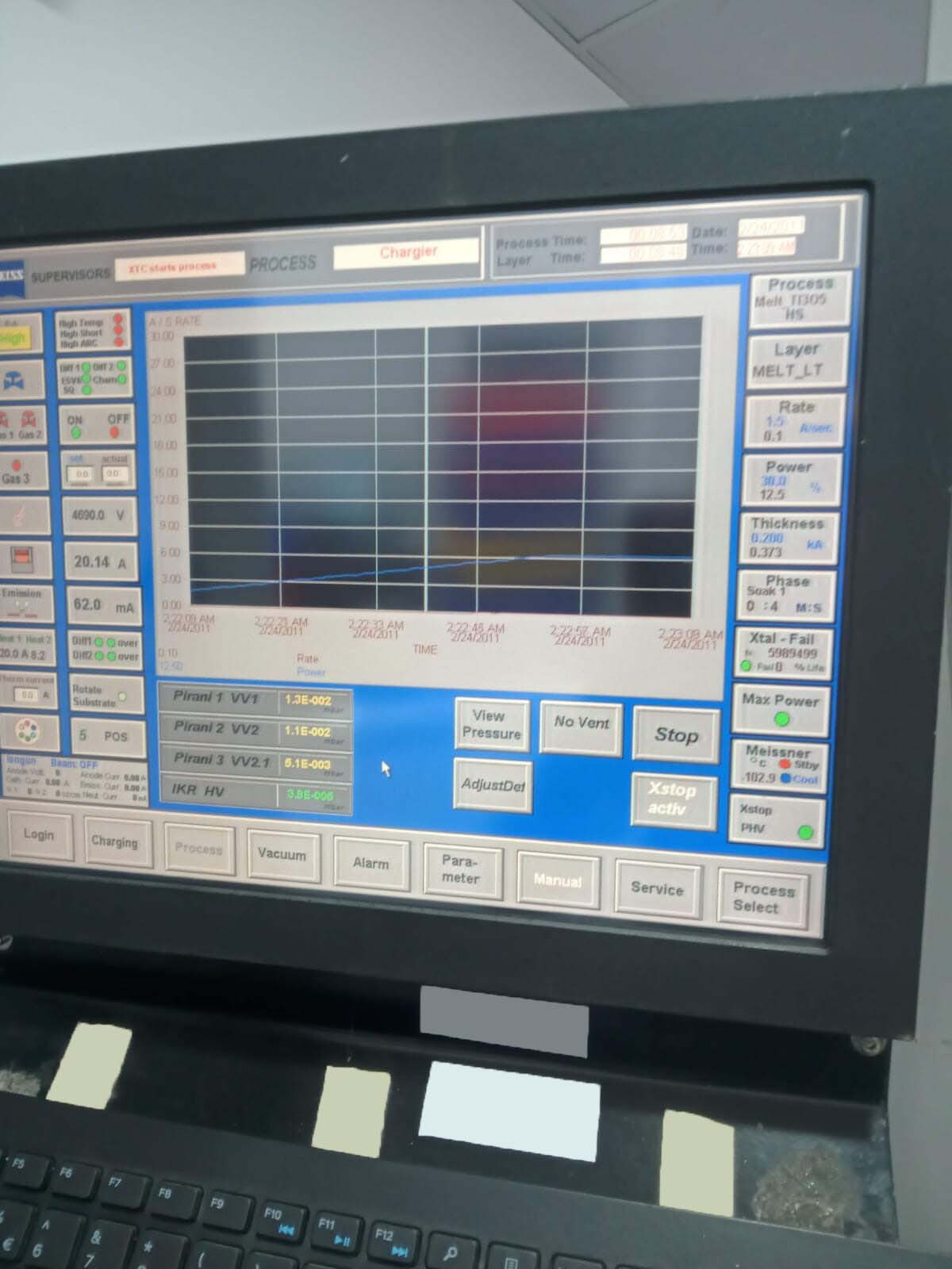
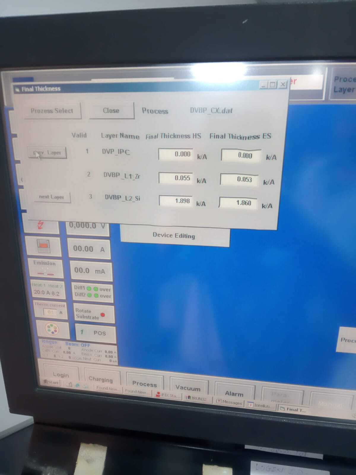
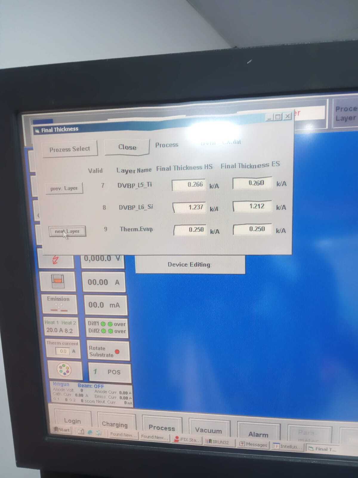
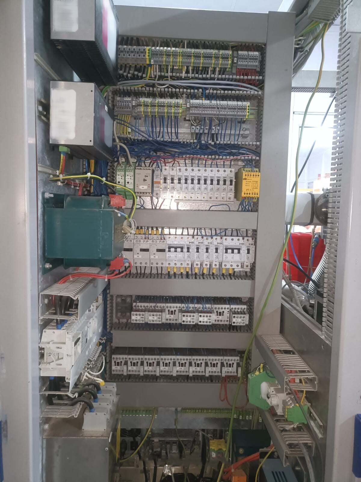
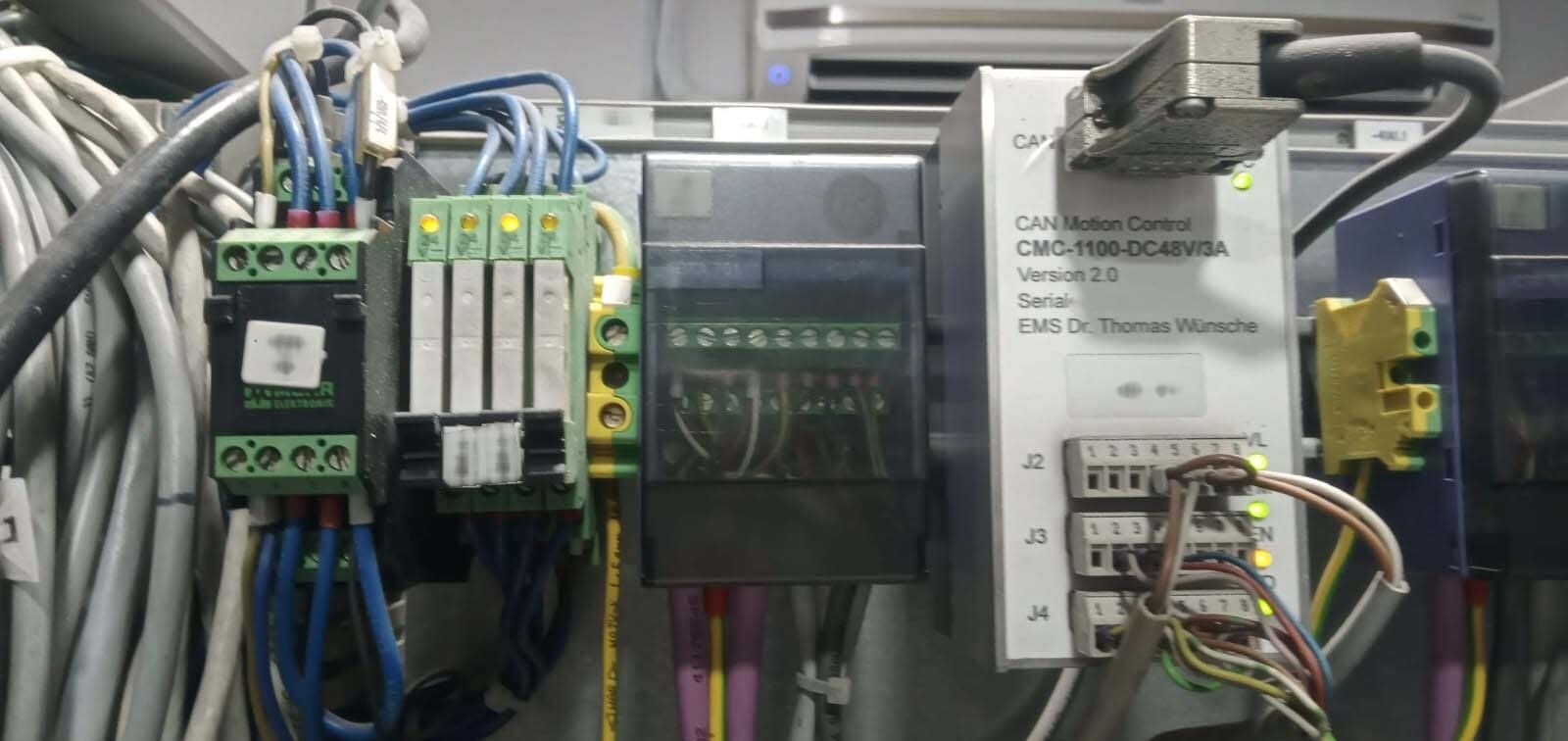
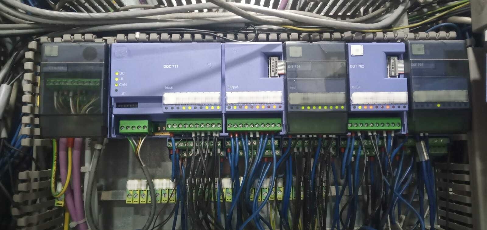
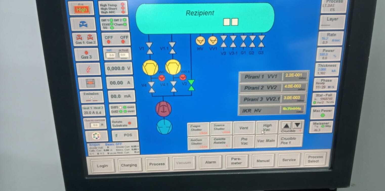
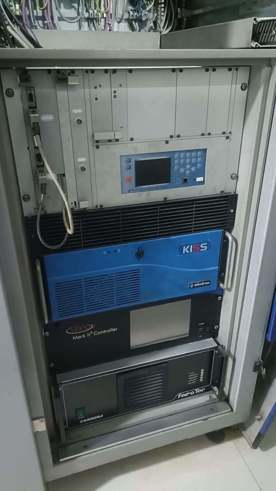
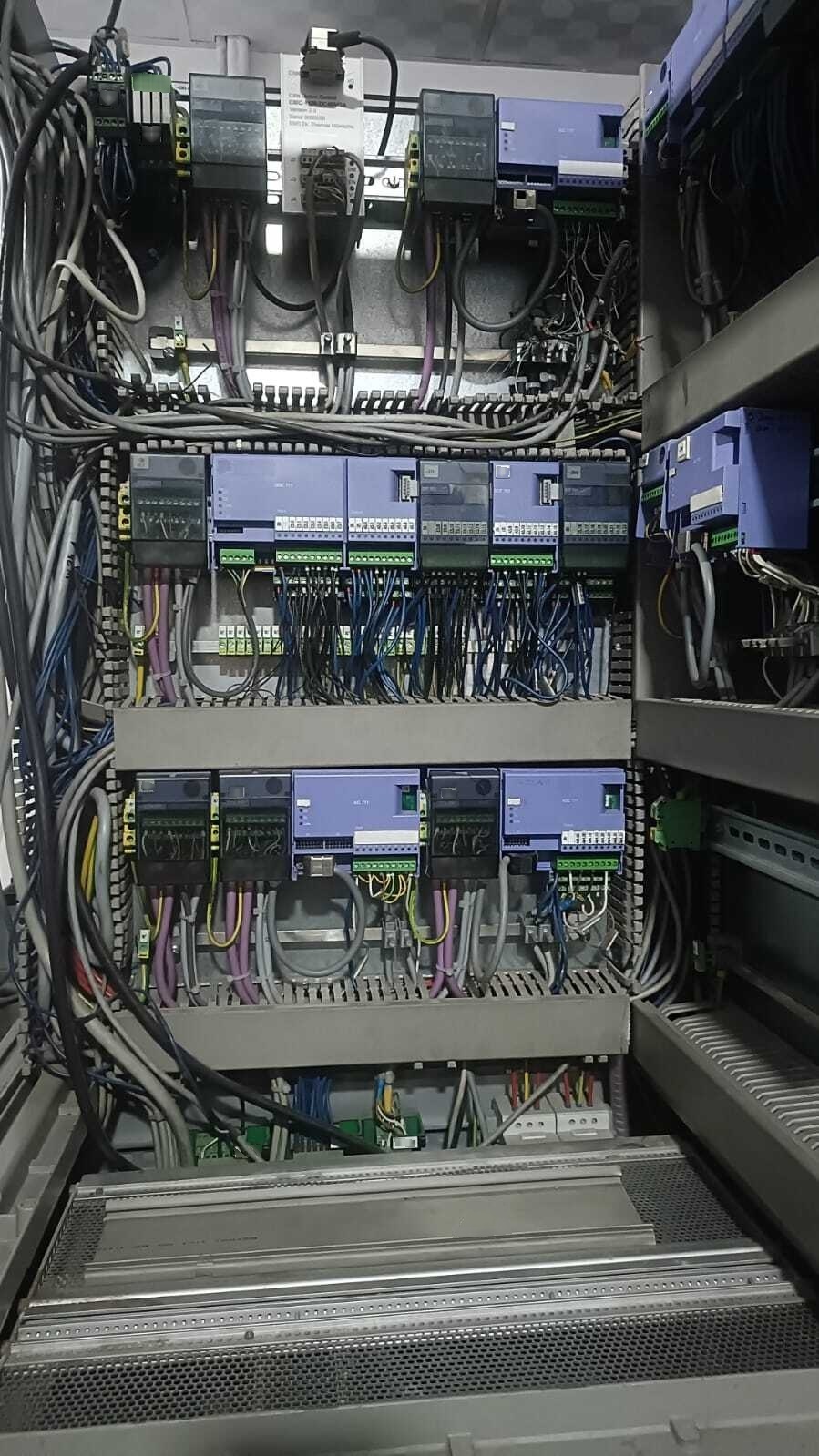
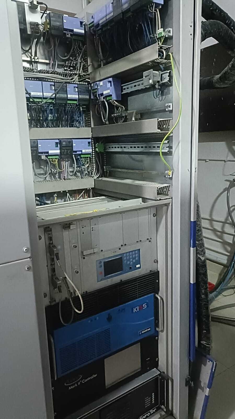
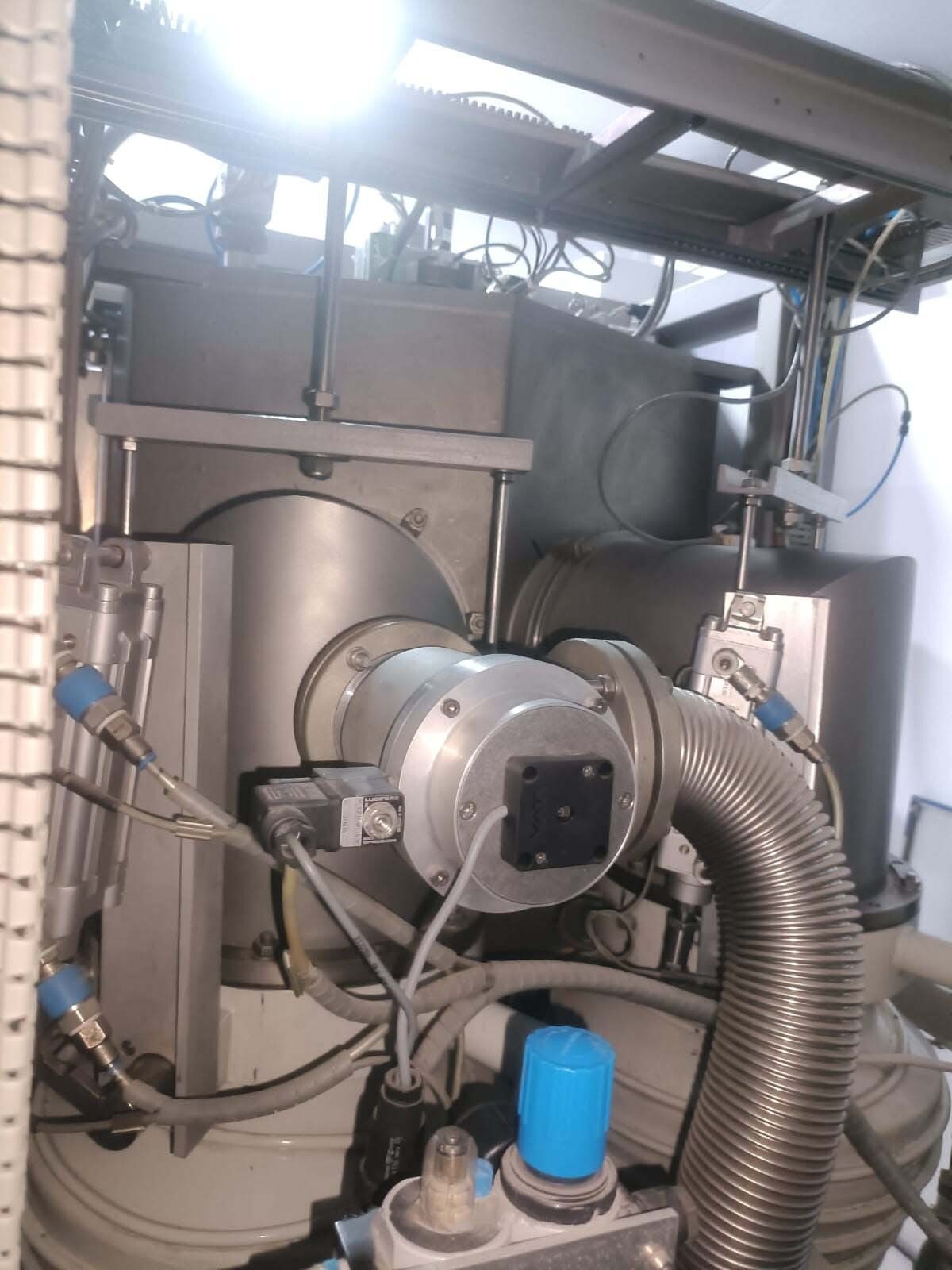
AR Coater system
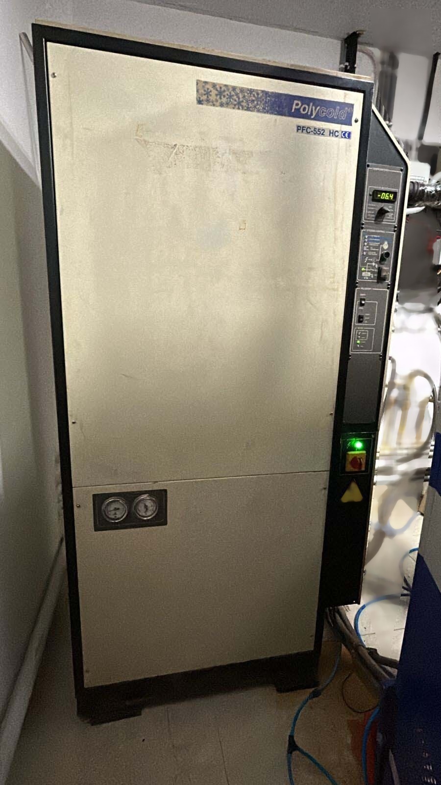
POLYCOLD PFC 552 HC Cryo system
POLYCOLD Chiller
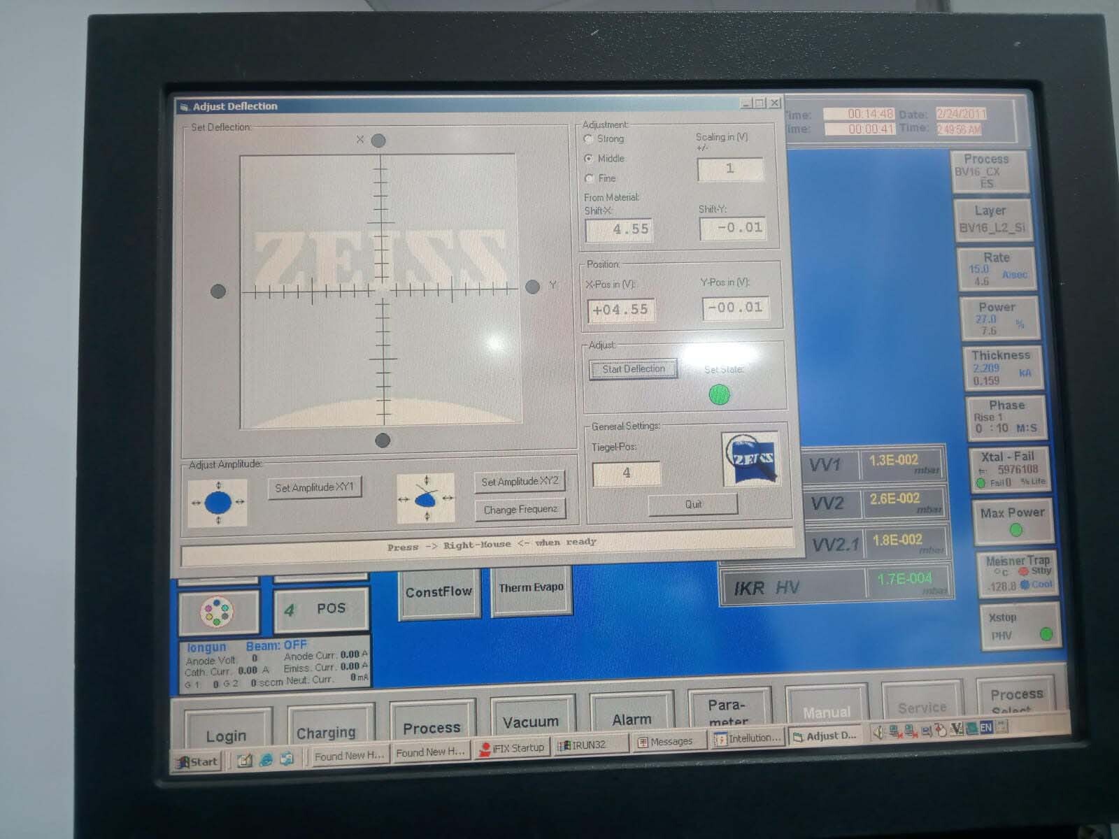
Electron and ion beam gun:
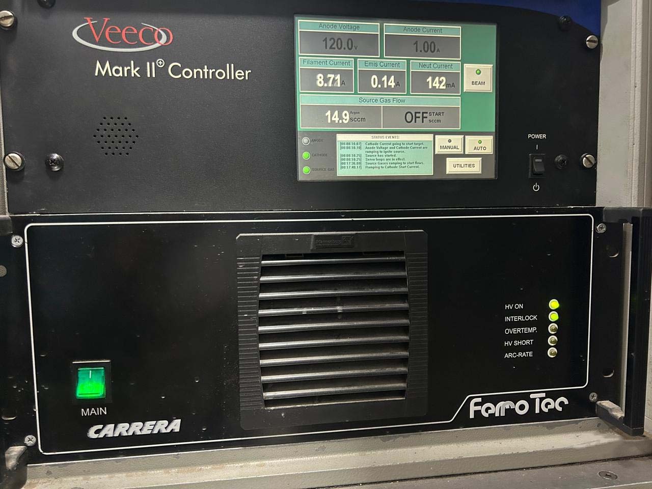
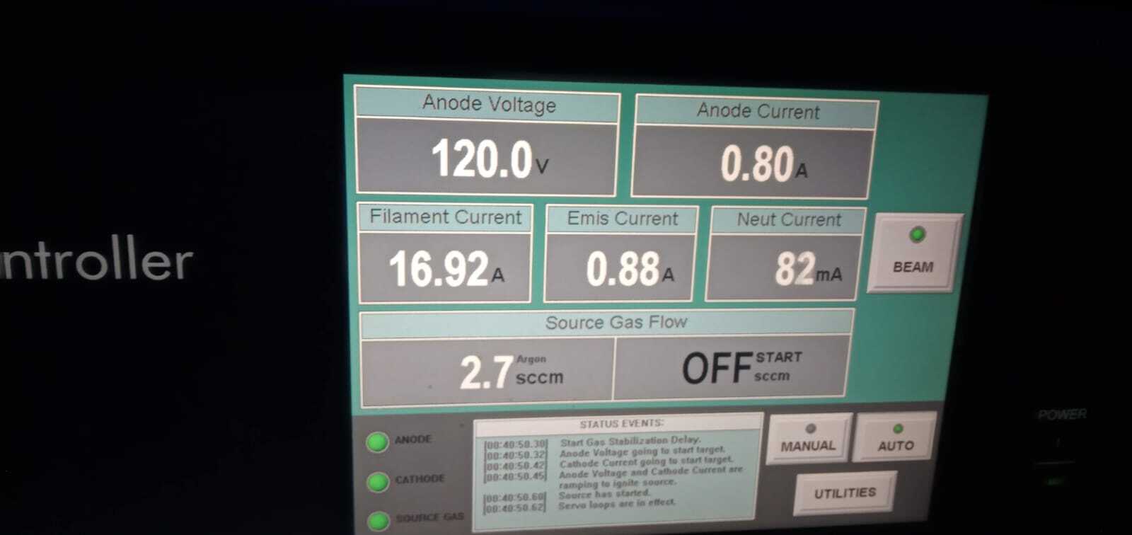
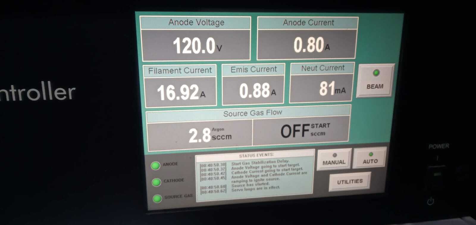
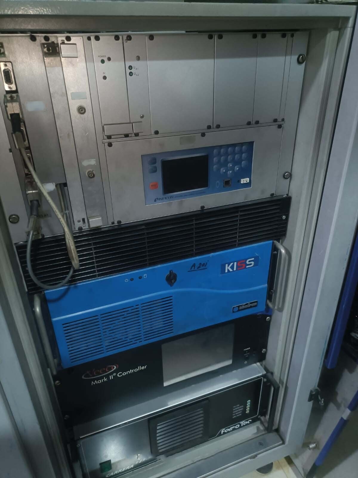
Mark II Plus Ion gun
Ferrotech Gun supply
Pumping system:
LEYBOLD Vacuum pump
Booster pump
Depositing meterial:
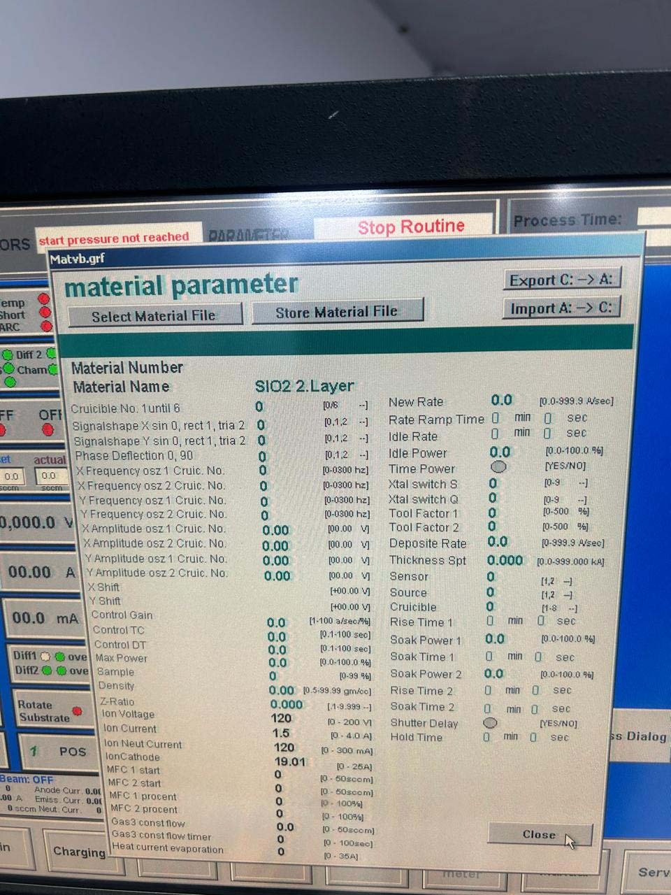
Sio2
Zro2
Ti3o5
ITO
Super hydrophobic
Operating system: Windows XP.
ZEISS A20 is a state-of-the-art photoresist equipment manufactured by ZEISS, a renowned German company specializing in optical systems and precision technology. This advanced system is designed for high-resolution lithography processes used in the semiconductor industry, specifically for the patterning of photoresist materials on substrates to create intricate patterns and structures on microelectronics devices. At the core of A20 unit is its sophisticated optics and precision components, which enable it to achieve submicron resolution levels necessary for cutting-edge semiconductor manufacturing. The machine features a high-precision alignment stage with sub-nanometer positioning accuracy, allowing for the precise placement of masks and substrates during exposure. This level of precision is crucial for achieving tight overlay tolerances and pattern fidelity in the final devices. One of the key components of ZEISS A20 tool is its advanced light source technology, which typically utilizes deep ultraviolet (DUV) or extreme ultraviolet (EUV) light sources for exposing the photoresist material. These light sources provide the precise wavelength and intensity of light required to expose the photoresist with high resolution and fidelity. The asset also includes advanced optics such as projection lenses and beam shaping elements to focus and shape the light for optimal patterning performance. A20 model is equipped with a sophisticated control equipment that allows users to define and optimize exposure parameters such as dose, focus, and alignment for each layer of the lithography process. The system can also perform advanced process corrections and compensations to account for factors like lens aberrations, substrate topography, and mask distortions, ensuring high-quality patterning across the entire wafer surface. In addition to its imaging capabilities, ZEISS A20 unit incorporates advanced process monitoring features to ensure the quality and consistency of the lithography process. These features may include in-situ metrology tools for measuring critical dimensions in real-time, as well as advanced feedback control algorithms to adjust exposure parameters on-the-fly based on the measured data. This real-time monitoring and control capability enable the machine to detect and correct process variations before they impact device performance. Furthermore, A20 tool is designed with modularity and flexibility in mind, allowing users to adapt the asset to different process requirements and emerging technologies. The model may support multiple exposure techniques such as binary mask, phase-shifting mask, and multi-patterning schemes, enabling users to address a wide range of lithography challenges in advanced semiconductor manufacturing. Overall, ZEISS A20 photoresist equipment represents a cutting-edge solution for high-resolution lithography applications in the semiconductor industry. With its advanced optics, precise control capabilities, and process monitoring features, the system enables users to achieve the stringent patterning requirements of modern semiconductor devices while maintaining high productivity and yield.
There are no reviews yet