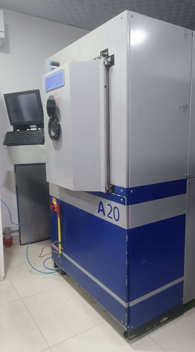
Used ZEISS A20 #293819007 for sale
URL successfully copied!
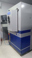



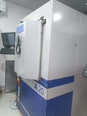
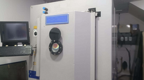
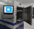



































Tap to zoom

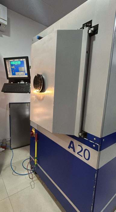
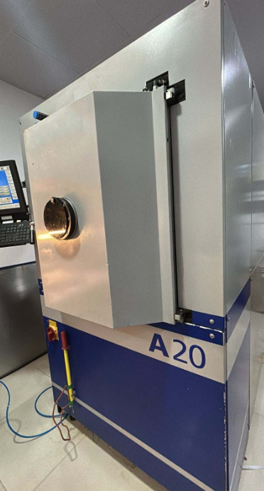
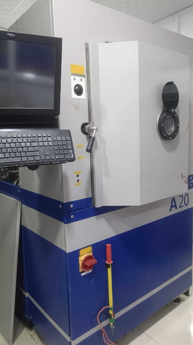
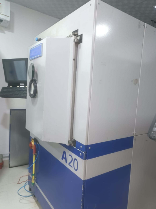
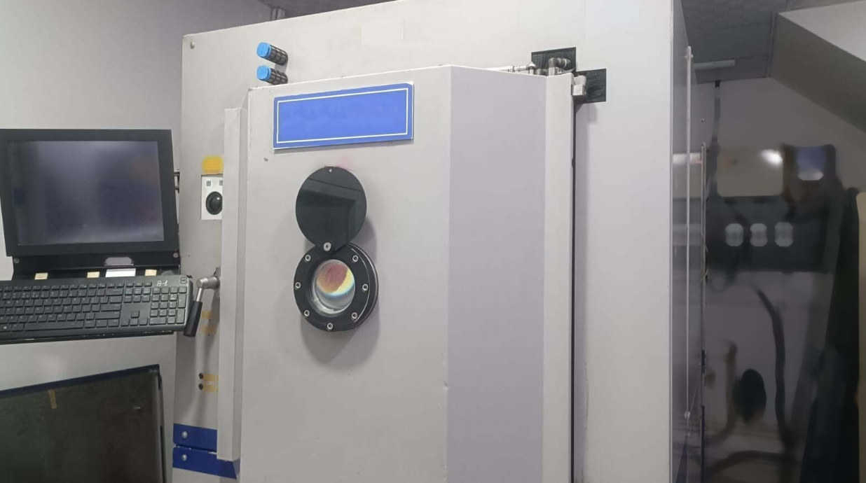
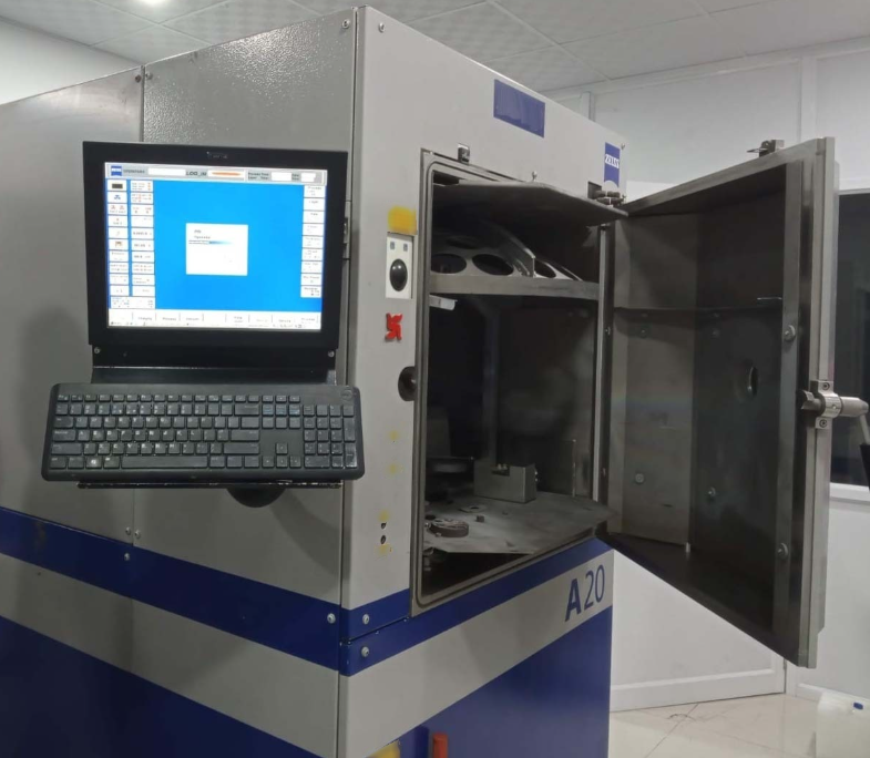
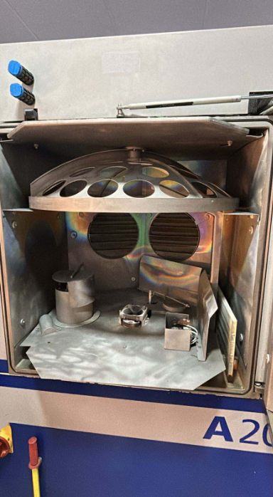
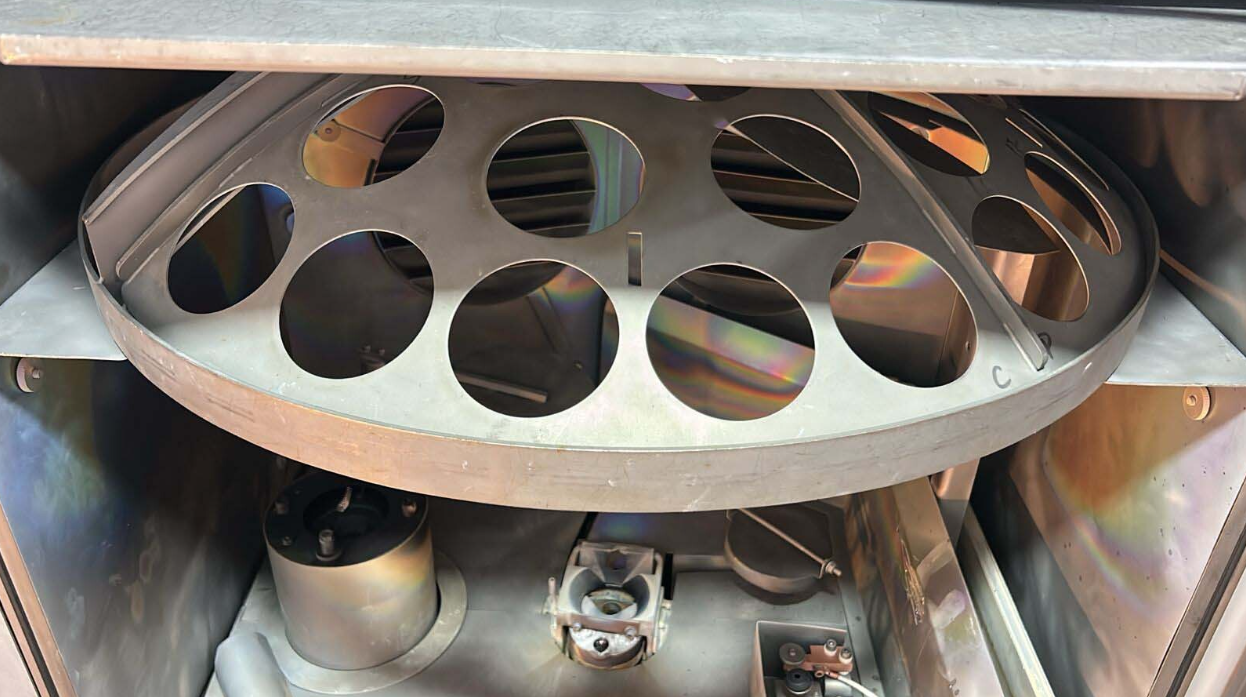
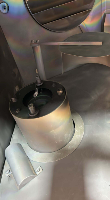
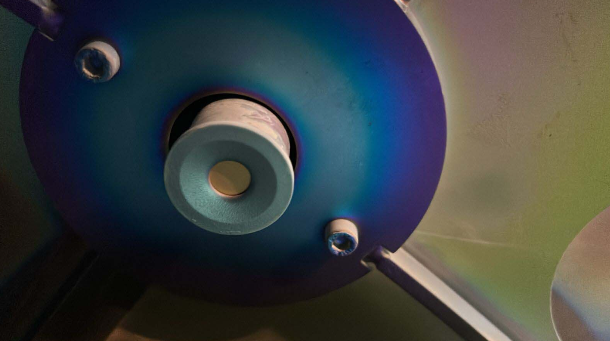
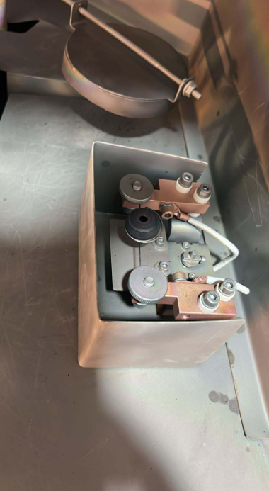
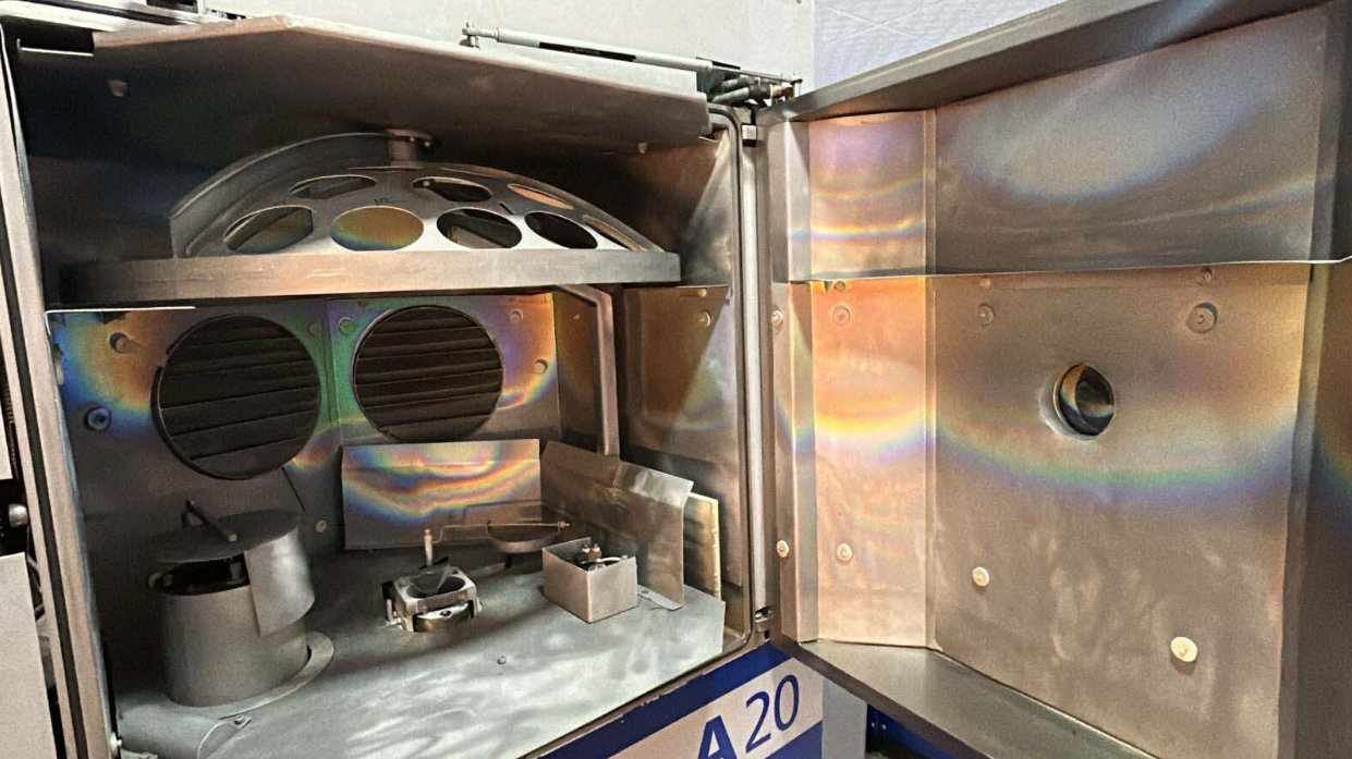

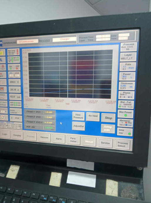
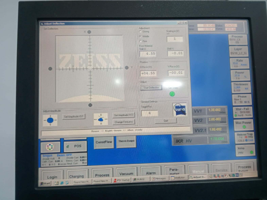
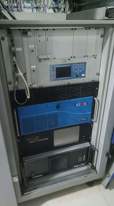
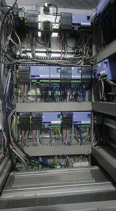
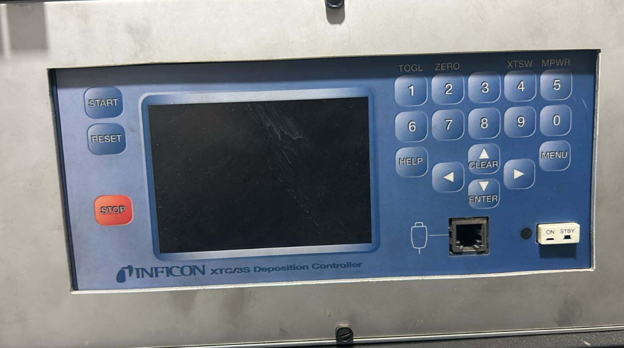
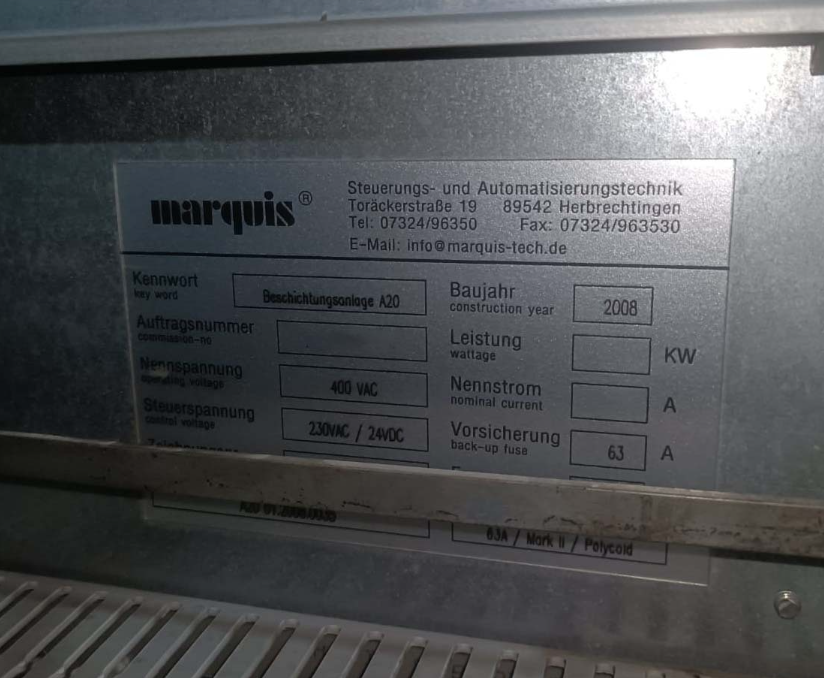
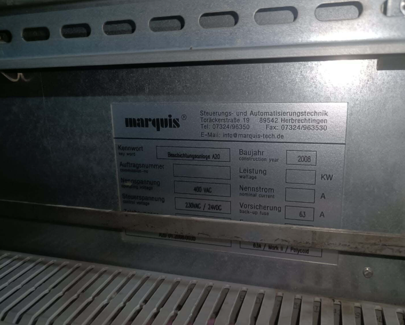
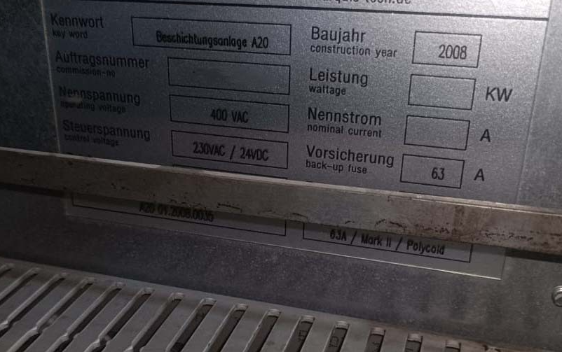
ID: 293819007
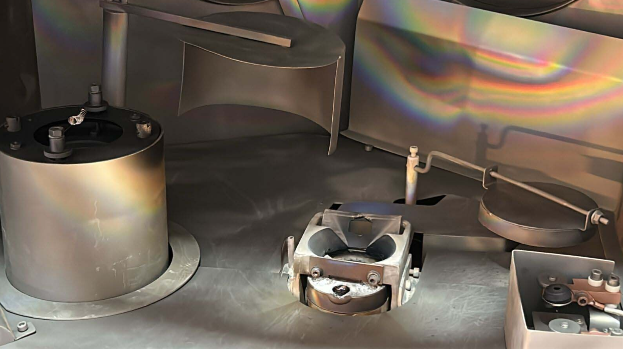
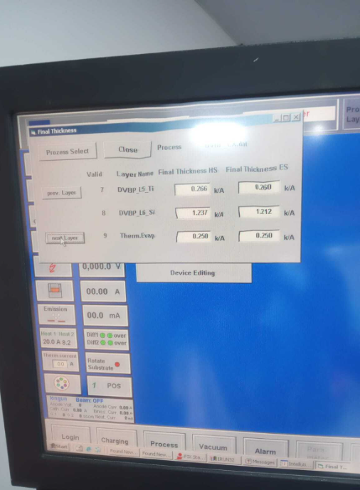
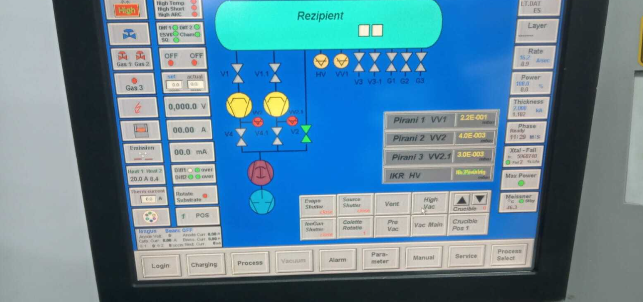
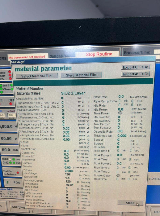
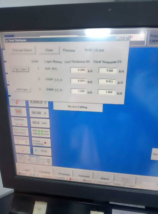
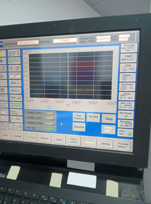
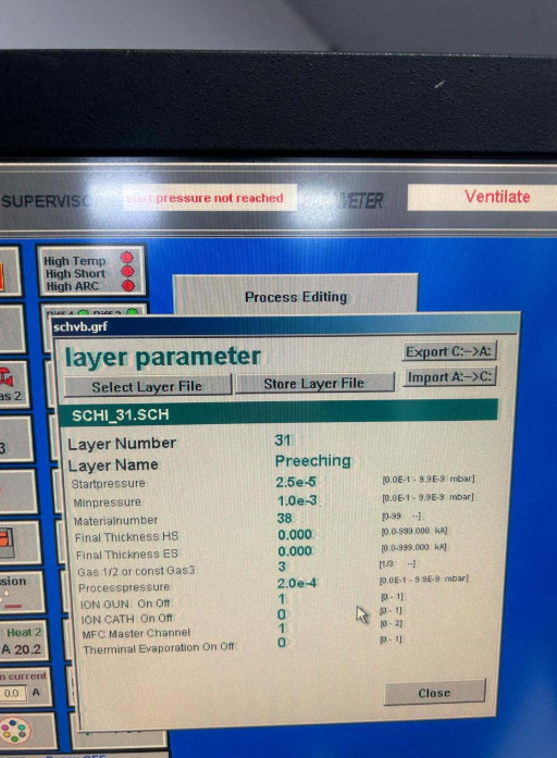
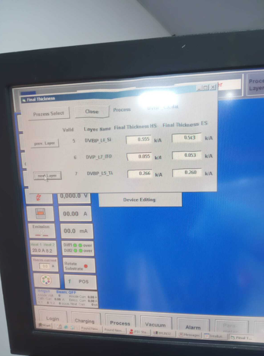
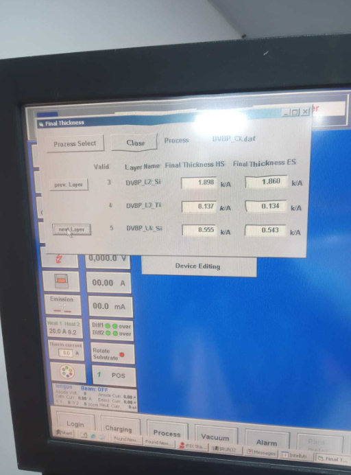
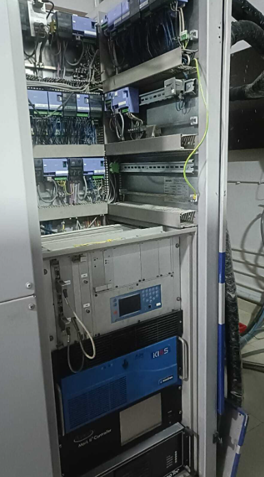
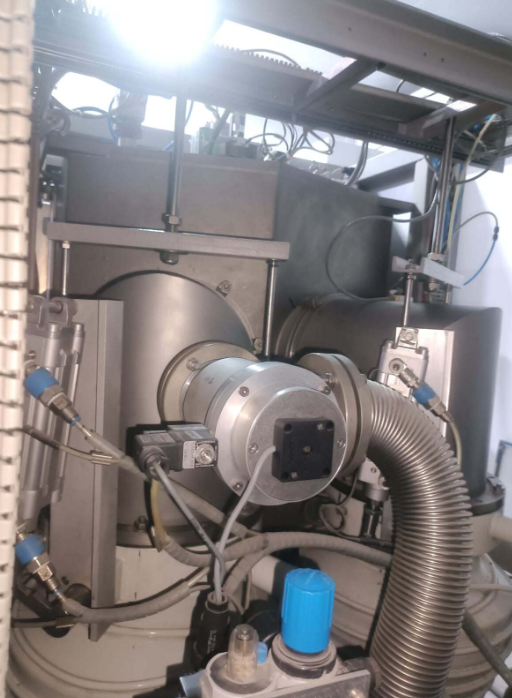
AR Coater system
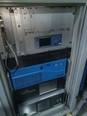
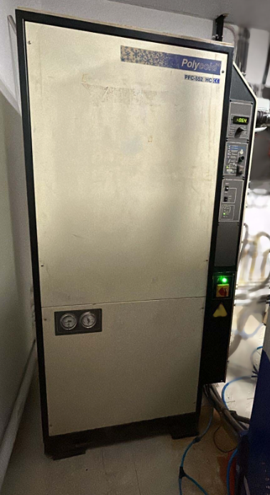
POLYCOLD PFC 552 HC Cryo system
Ultimate temp: ~146
POLYCOLD Chiller
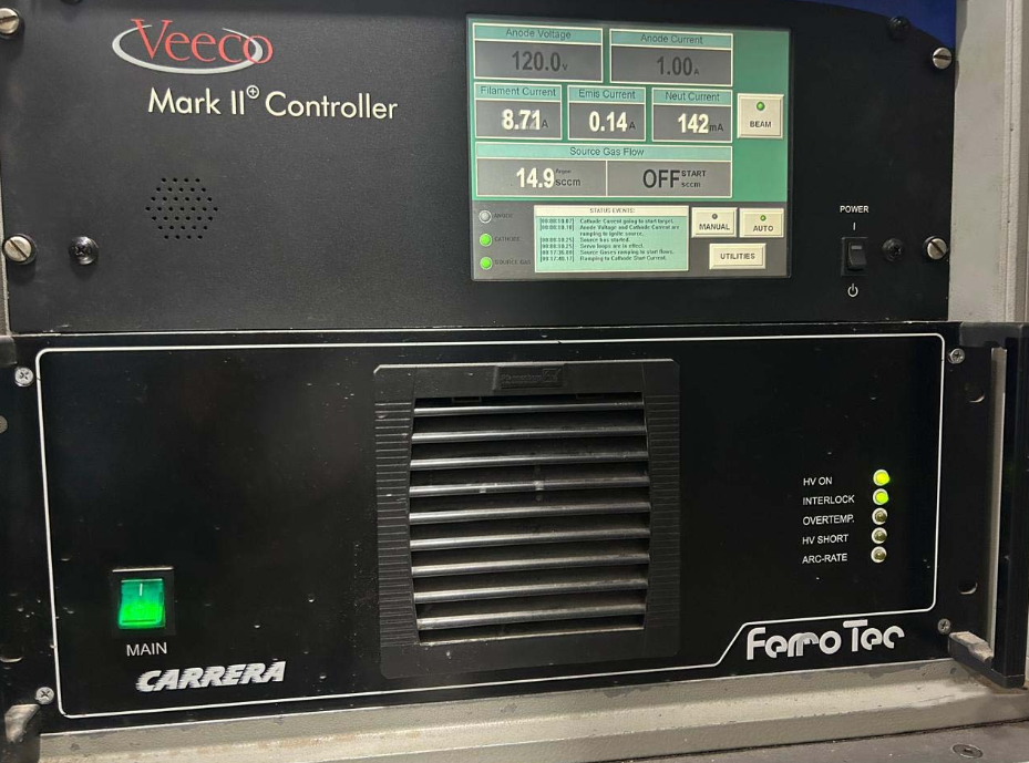
Electron and ion beam gun:
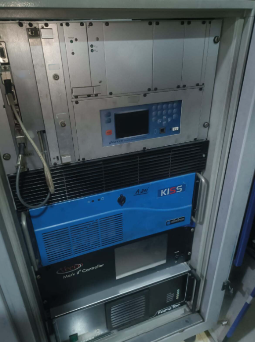
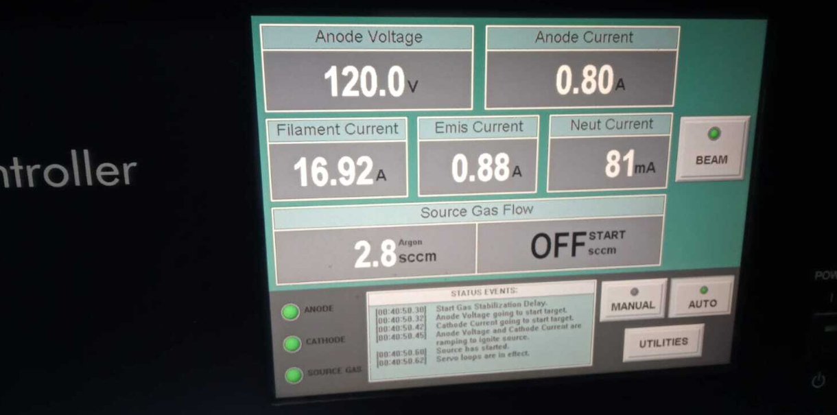
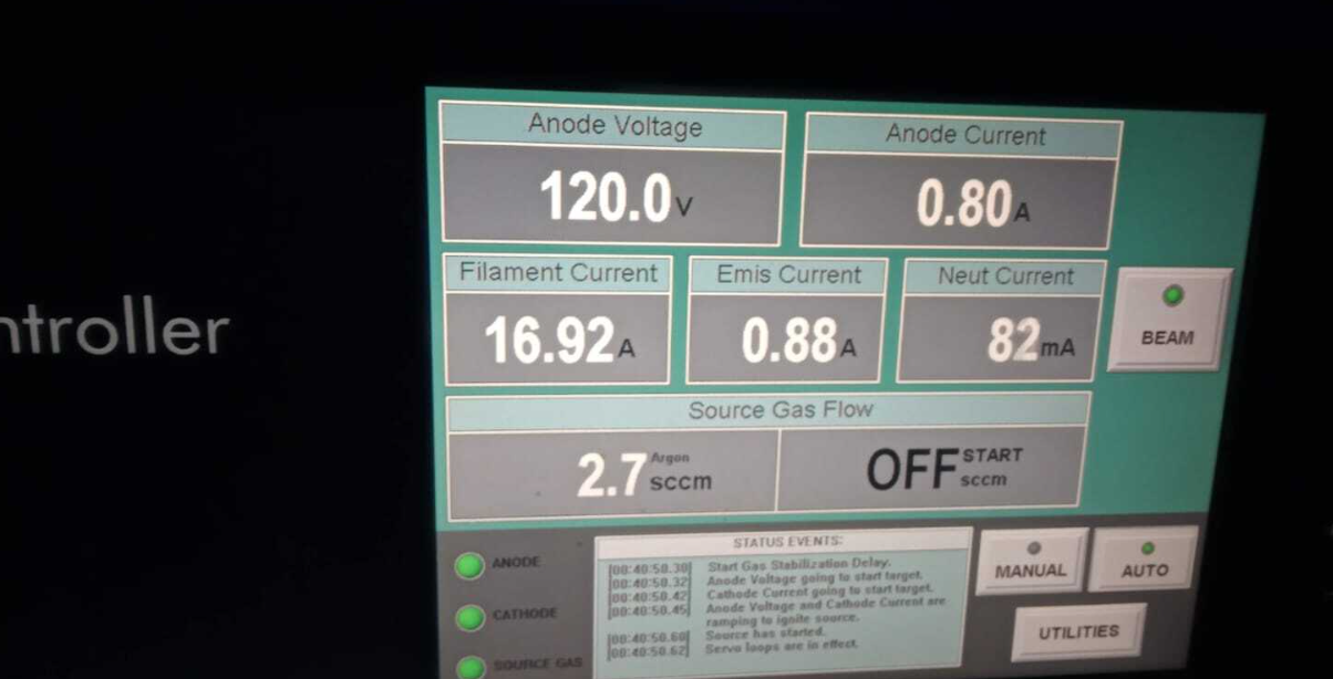
Mark II Plus Ion gun
Ferrotech Gun supply
Pumping system:
LEYBOLD Vacuum pump
Booster pump
Depositing material:
Sio2
Zro2
Ti3o5
ITO
Super hydrophobic
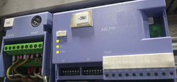
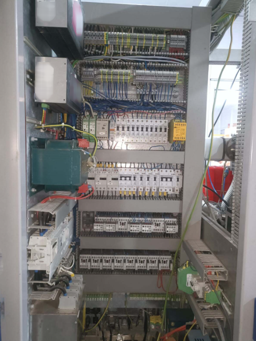
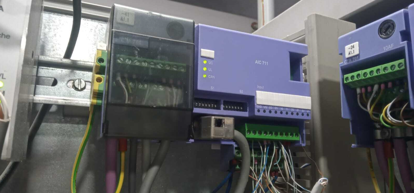
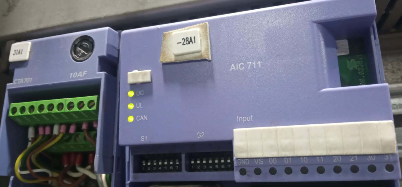
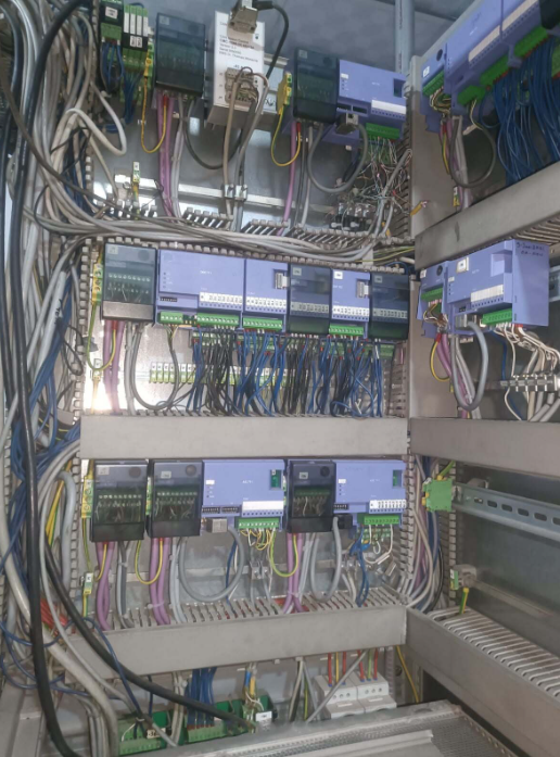
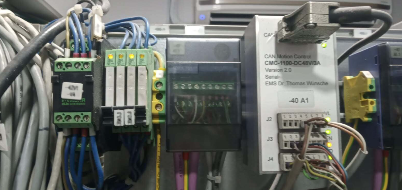
Known issues: Electrical tripping problem in 24vdc
Operating system: Windows XP.
ZEISS A20 photoresist equipment is an advanced tool used in semiconductor fabrication processes to transfer circuit patterns onto silicon wafers with high precision and efficiency. Developed by ZEISS, a renowned manufacturer of optical systems and equipment, A20 system is designed to meet the demanding requirements of the semiconductor industry for producing intricate and complex semiconductor devices used in various electronic applications. At the core of ZEISS A20 unit is its sophisticated lithography technology, which enables the precise patterning of photoresist materials on semiconductor substrates. Photoresist is a light-sensitive material that undergoes chemical changes when exposed to light, allowing the transfer of patterns onto the substrate for subsequent etching and other processing steps. A20 machine incorporates advanced optics, precise alignment mechanisms, and robust automation features to ensure accurate and repeatable patterning of photoresist layers with sub-micron resolution. One of the key features of ZEISS A20 tool is its high-resolution projection optics, which enable the precise focusing of light onto the photoresist layer to create intricate patterns with fine feature sizes. The asset uses a series of lenses, mirrors, and beam splitters to control the shape, intensity, and wavelength of the light source, providing flexibility in patterning different types of photoresist materials and structures. The high-quality optics of A20 model ensure uniform exposure across the entire substrate, resulting in consistent and reliable patterning outcomes. In addition to its advanced optics, ZEISS A20 equipment is equipped with a highly accurate alignment system that enables the precise registration of the pattern mask with the substrate. Alignment is critical in lithography processes to ensure that the desired pattern is transferred to the correct location on the substrate with minimal overlay errors. A20 unit utilizes sophisticated alignment sensors and algorithms to achieve sub-micron alignment accuracy, enabling the production of complex semiconductor devices with tight design tolerances. Moreover, ZEISS A20 machine features an intelligent automation tool that streamlines the lithography process and reduces operator intervention. The asset is equipped with advanced software control algorithms that optimize exposure parameters, focus settings, and alignment corrections in real-time to maximize throughput and yield. The automation capabilities of A20 model not only improve process efficiency but also reduce human errors and variability, resulting in higher process reliability and yield. Furthermore, ZEISS A20 equipment is designed for scalability and flexibility to accommodate a wide range of semiconductor manufacturing processes and applications. The system supports multi-layer patterning, double-sided exposure, and mask-to-wafer proximity lithography techniques, allowing semiconductor manufacturers to create complex device structures with high productivity and precision. The modular design of A20 unit enables easy integration into existing semiconductor fabrication lines and seamless adoption of new technologies and processes. Overall, ZEISS A20 photoresist machine is a state-of-the-art tool for semiconductor lithography applications, offering high resolution, accuracy, automation, and flexibility to meet the evolving demands of the semiconductor industry. With its advanced optics, precise alignment, intelligent automation, and scalability features, A20 tool empowers semiconductor manufacturers to achieve superior patterning results, improve process efficiency, and accelerate the development of cutting-edge semiconductor devices for various electronic applications.
There are no reviews yet