Used ZEISS A20 #293822914 for sale
URL successfully copied!
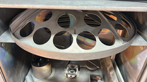

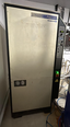




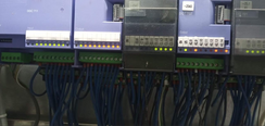
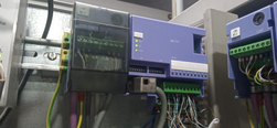

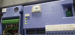
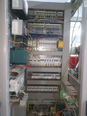
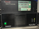
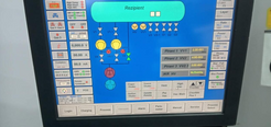
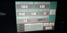
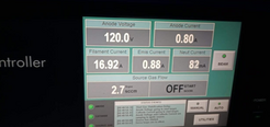
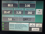

Tap to zoom
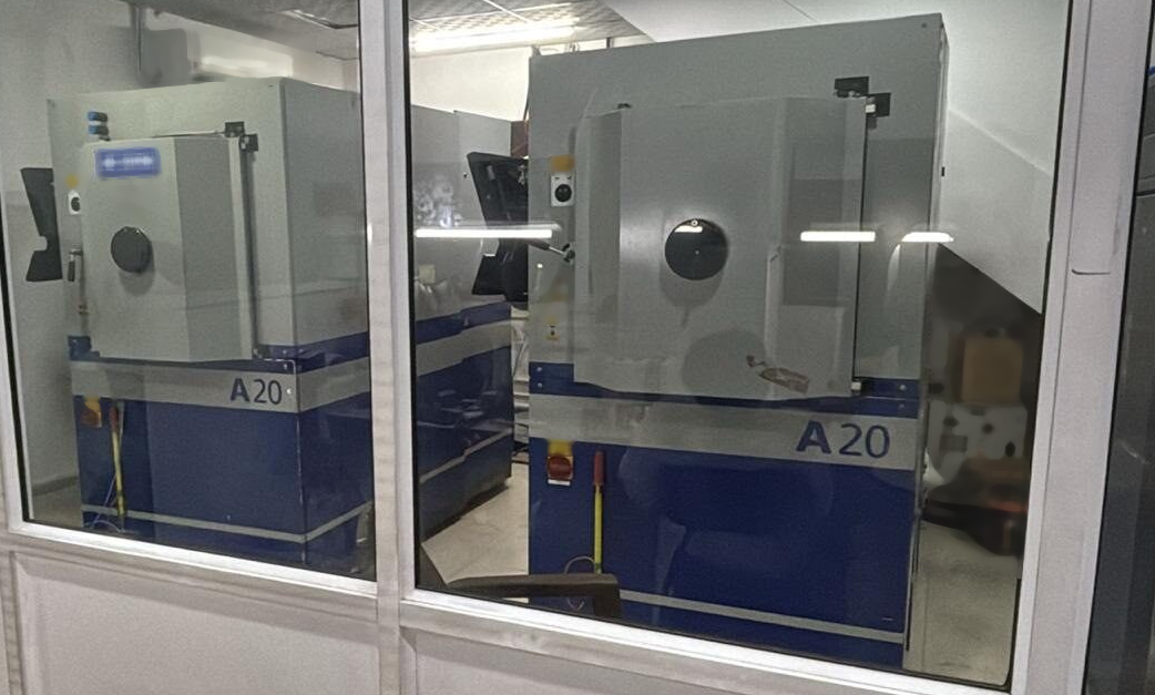

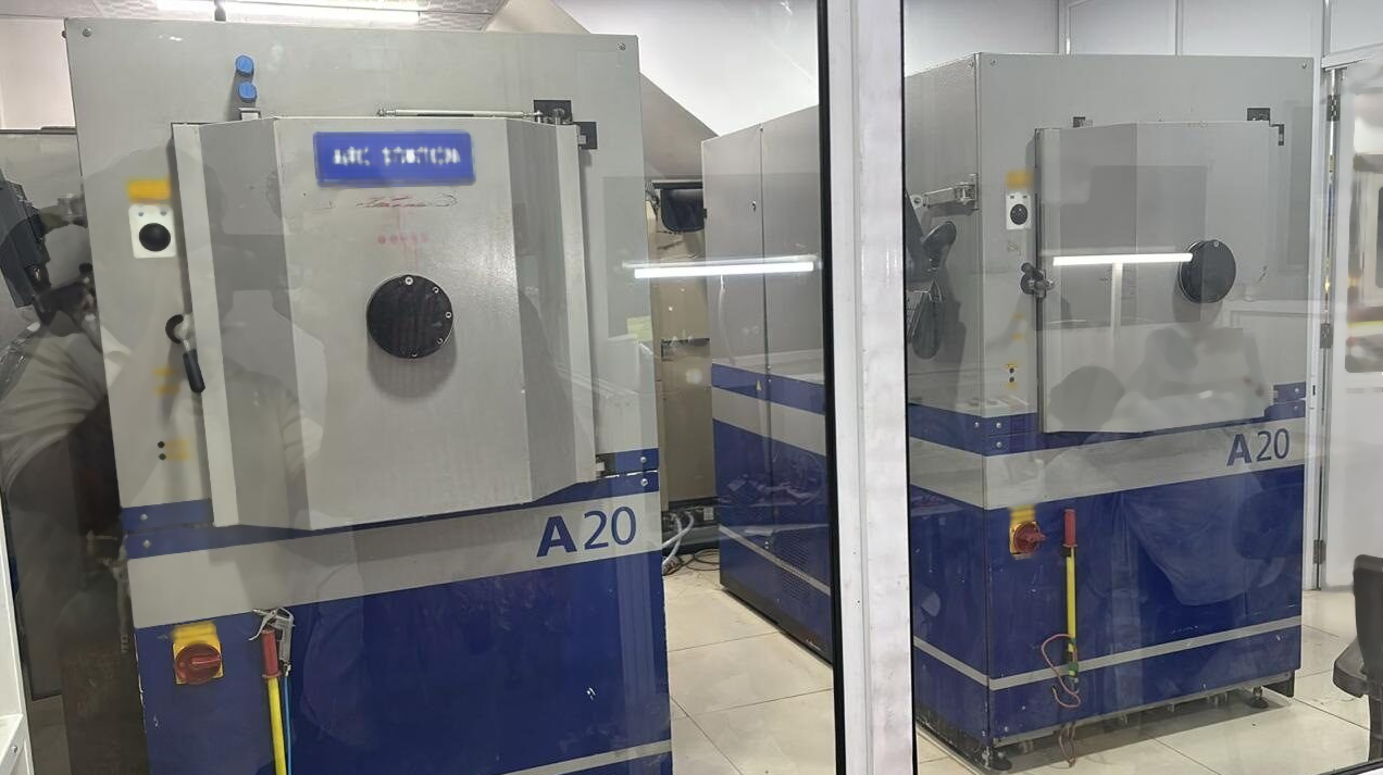
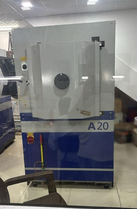
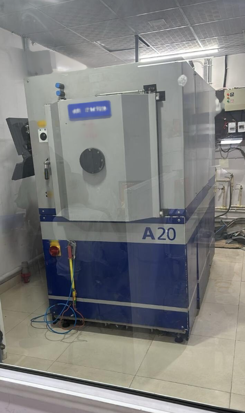
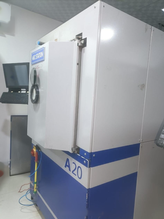
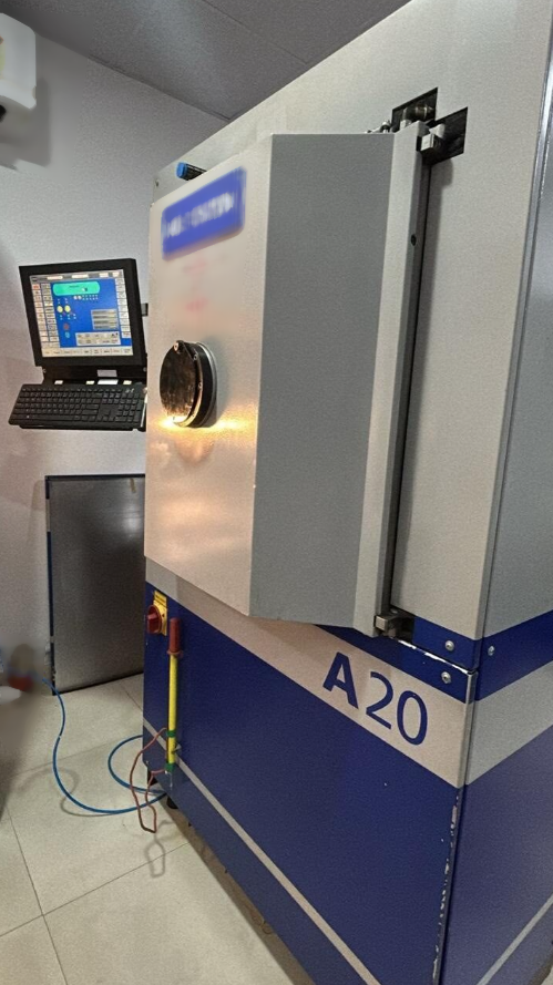
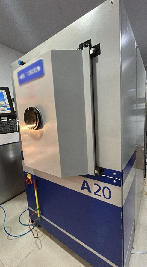
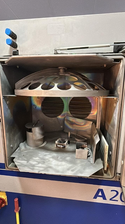
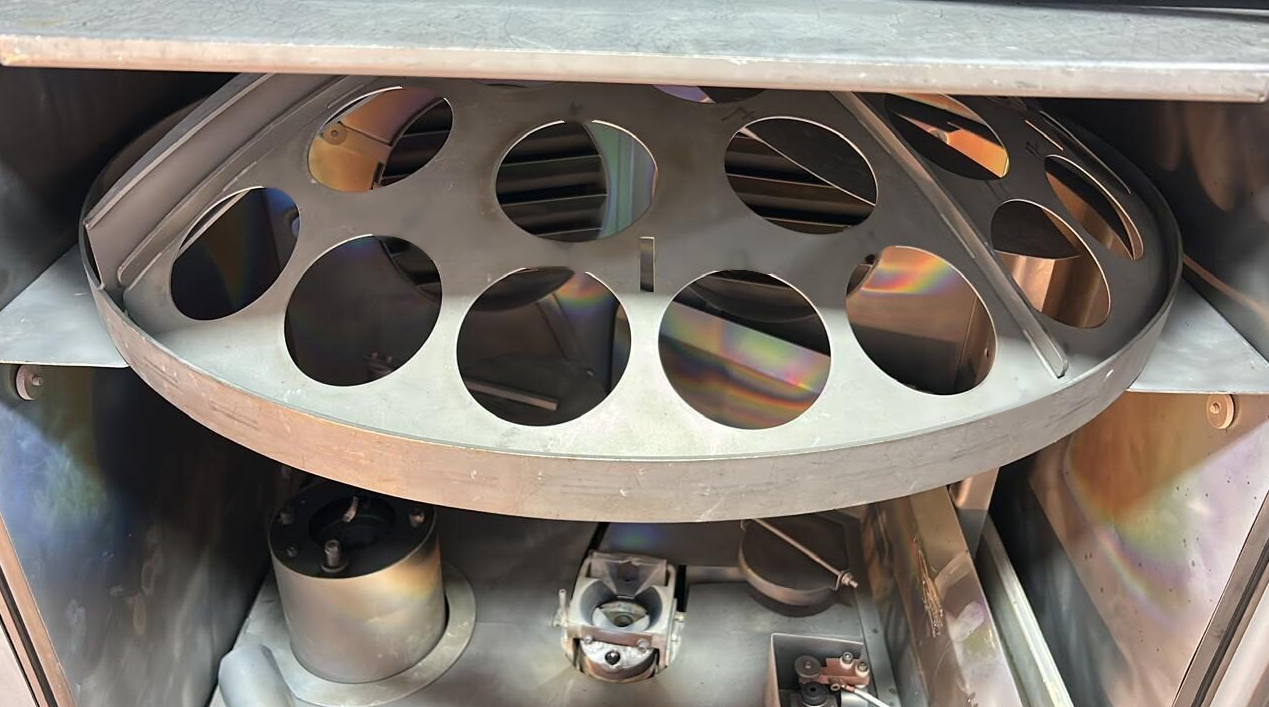
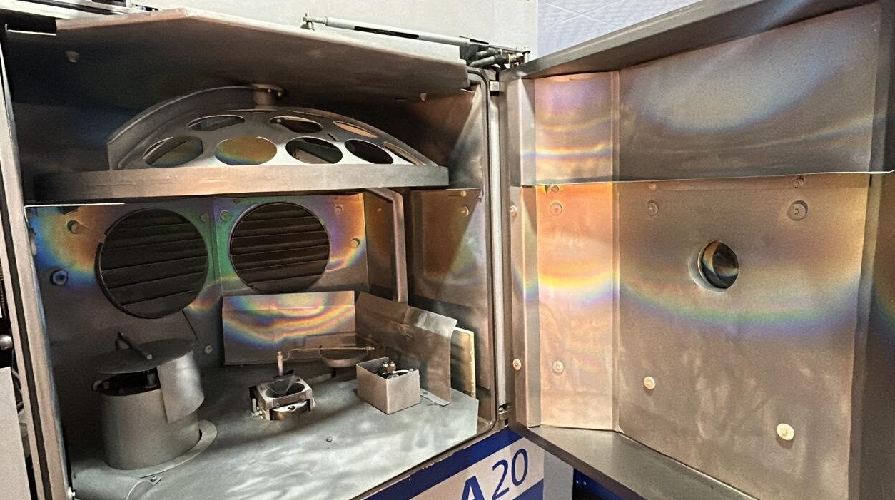
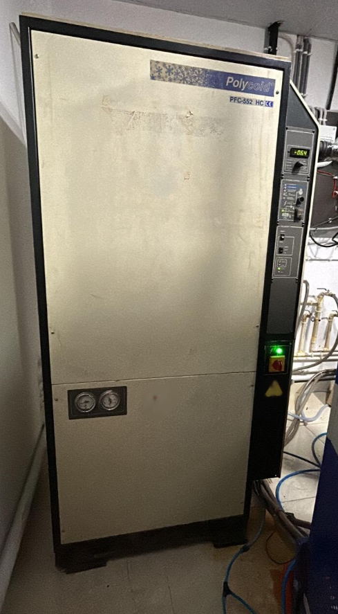
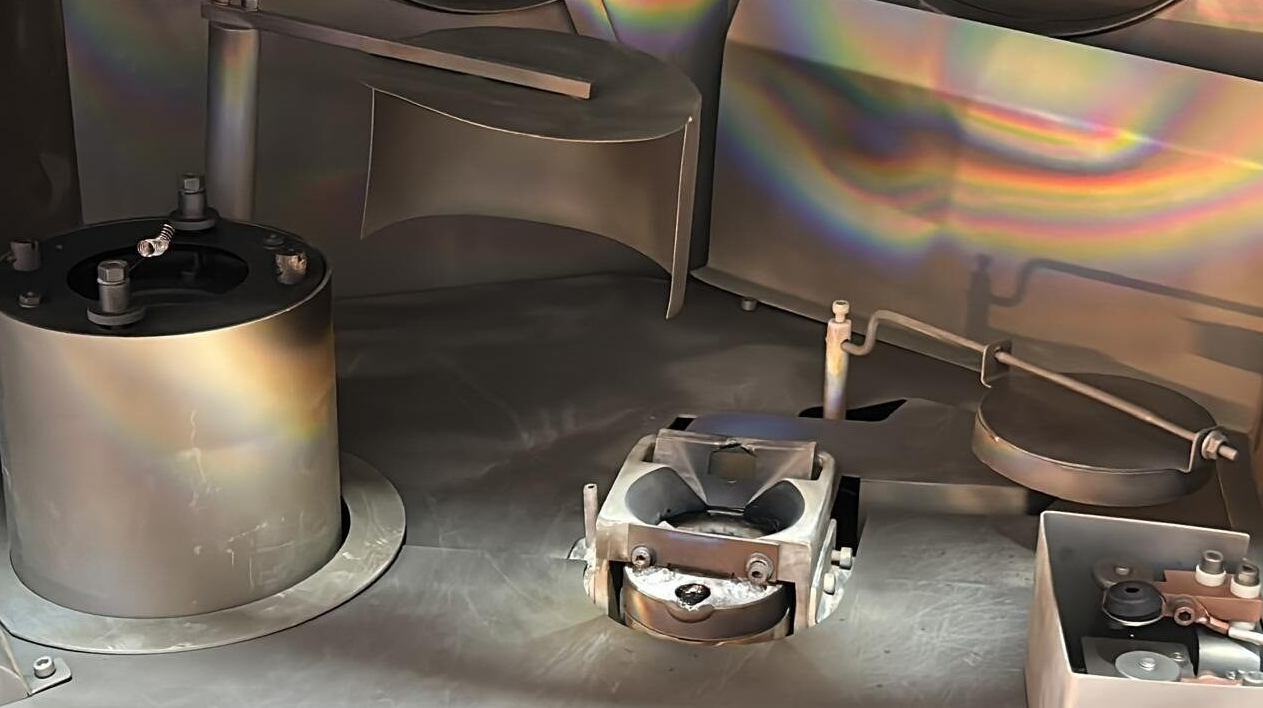
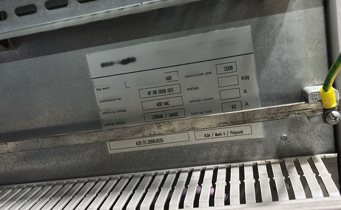
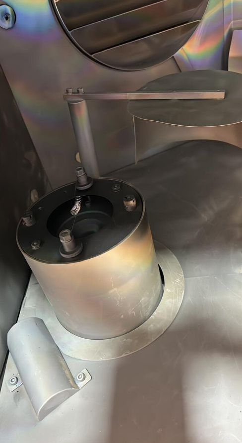
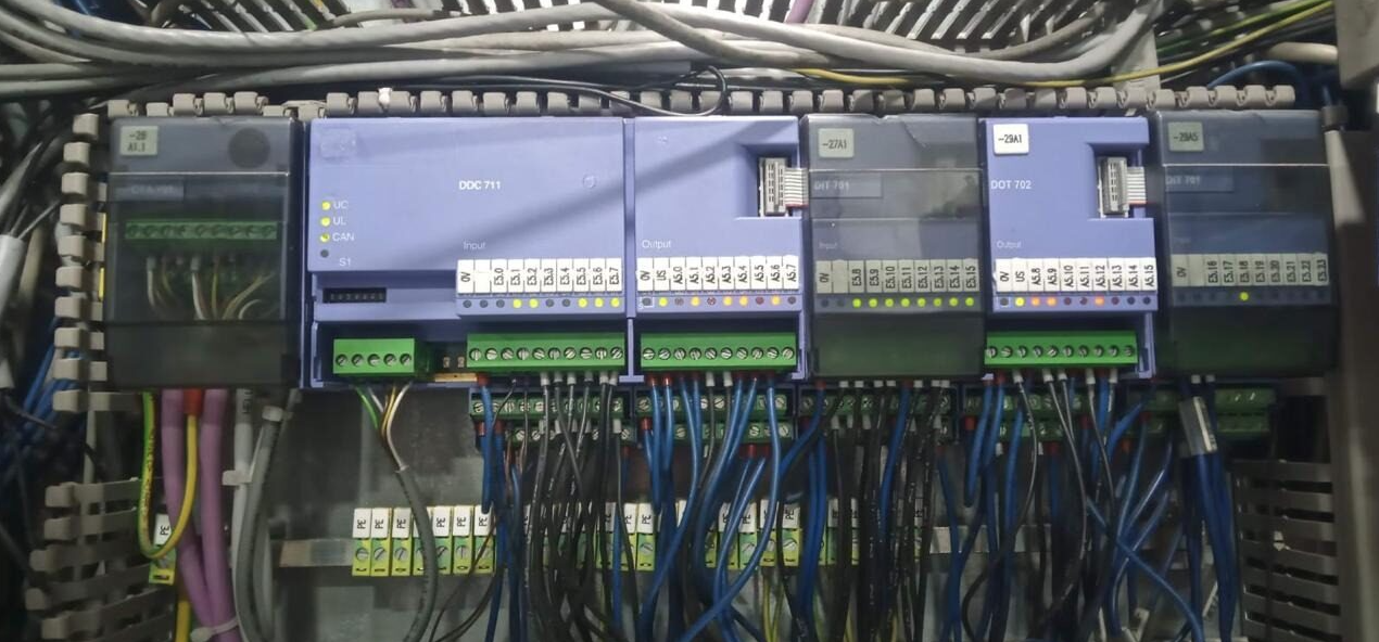
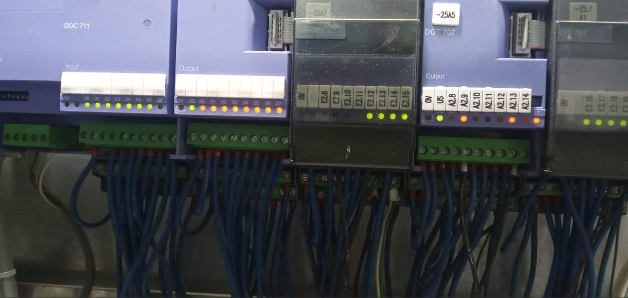
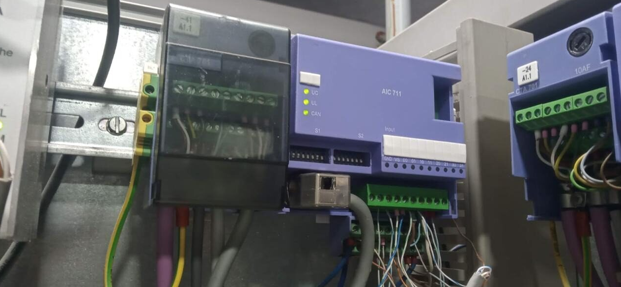
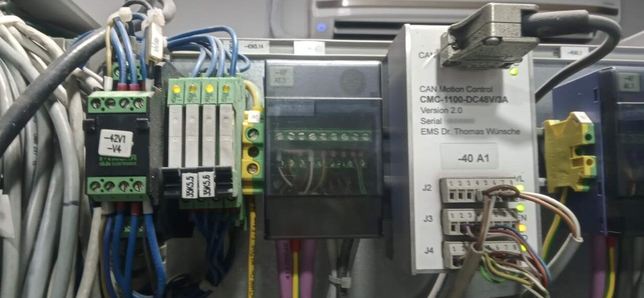
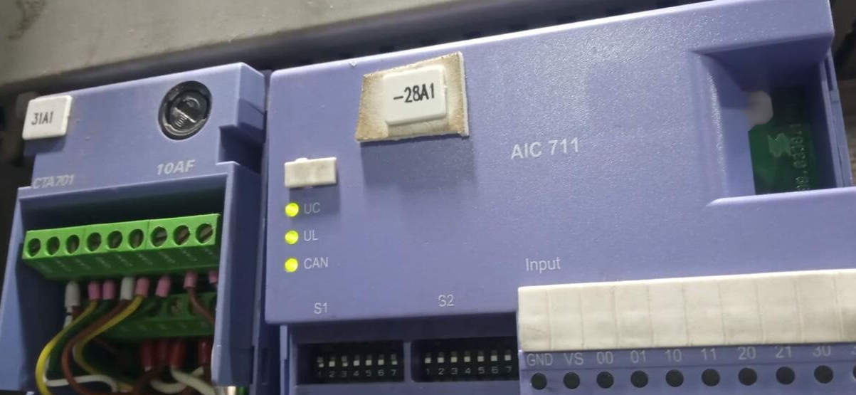
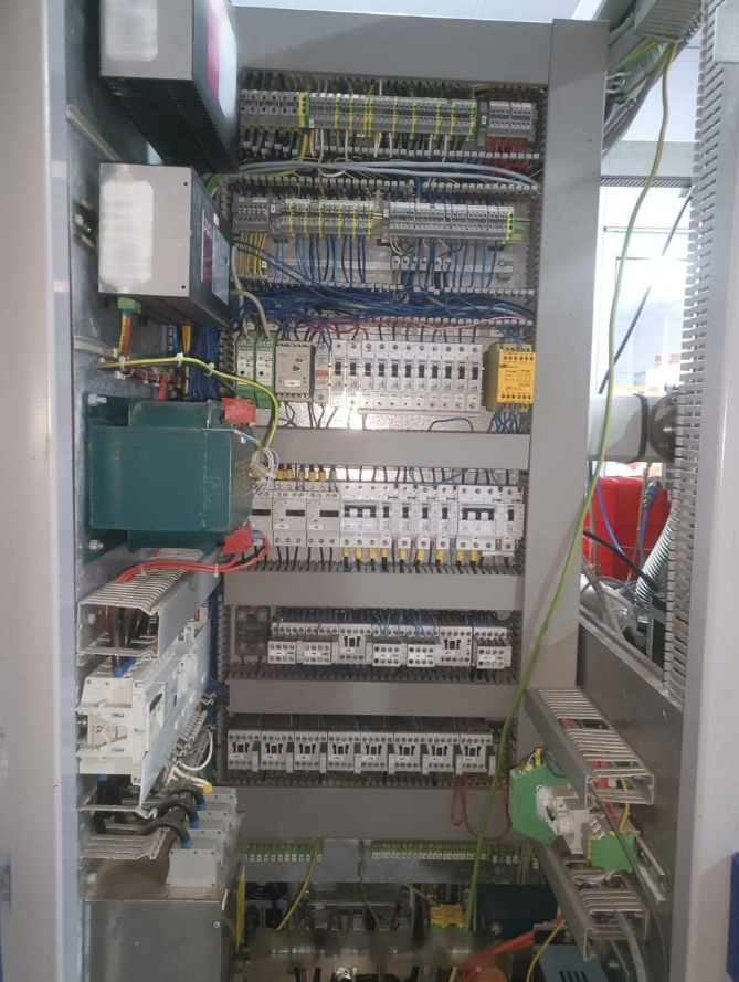
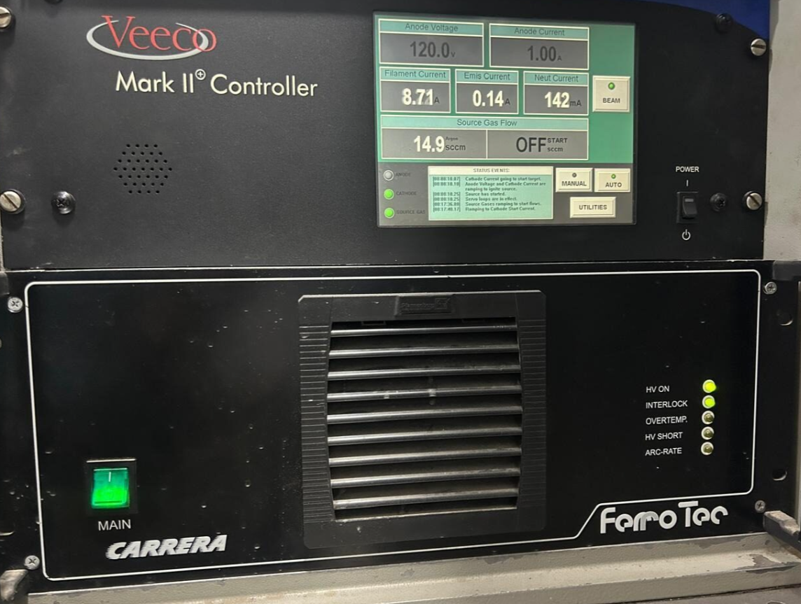
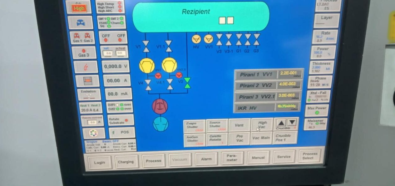
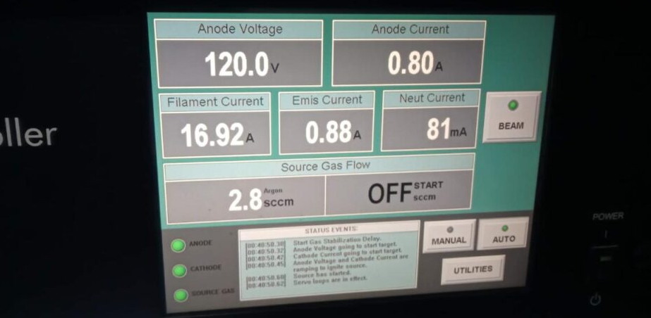
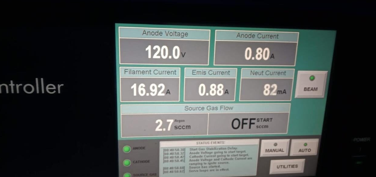
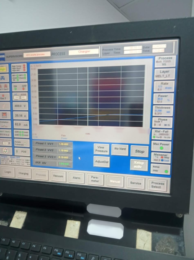
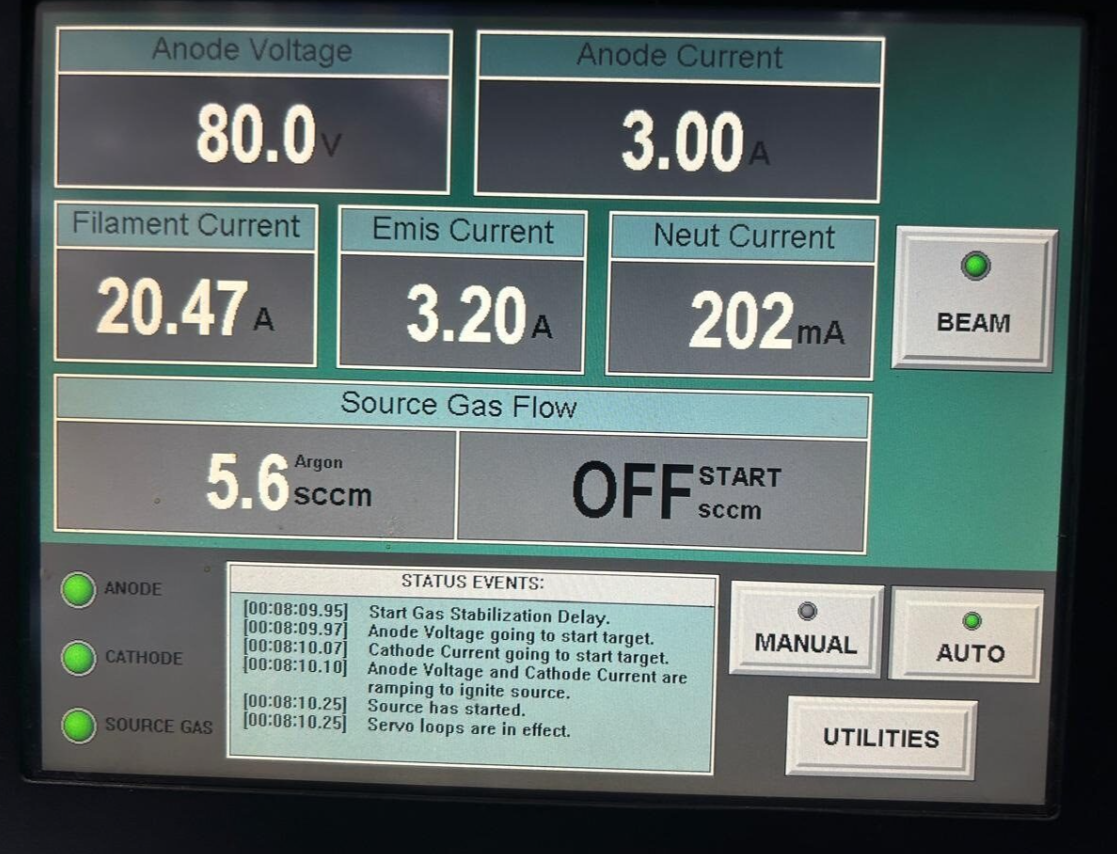
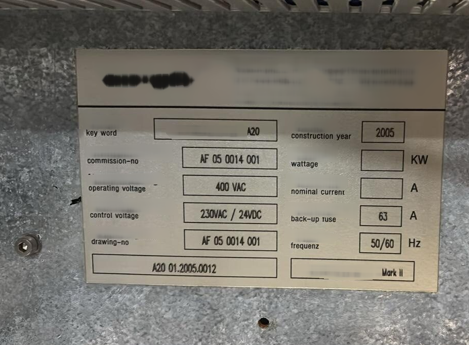
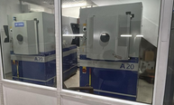
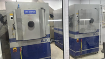
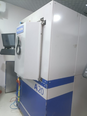
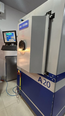
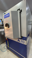
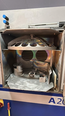
ZEISS A20 is a sophisticated photoresist equipment designed for precise and high-resolution photolithography processes in semiconductor manufacturing and research laboratories. This advanced system provides a comprehensive solution for transferring patterns onto substrates with exceptional accuracy and repeatability, making it an essential tool for the fabrication of integrated circuits, MEMS devices, sensors, and other microstructures. At the core of A20 unit is its advanced illumination and imaging capabilities, which are critical for defining intricate patterns on photoresist layers. The machine utilizes a high-intensity light source, such as a UV laser or mercury arc lamp, to expose the photoresist material on the substrate. The light is directed through a series of optical components, including lenses, mirrors, and filters, to precisely control the intensity, wavelength, and polarization of the light reaching the substrate. This meticulous control ensures that the desired patterns are accurately reproduced on the substrate with minimal distortion or aberrations. One of the key features of ZEISS A20 tool is its high-resolution imaging capabilities, which enable precise alignment and pattern definition on the substrate. The asset is equipped with a high-performance microscope objective or projection lens that allows for sub-micron resolution imaging of the photoresist patterns. This level of resolution is essential for creating intricate features and patterns on the substrate, such as transistor gates, interconnects, and sensor elements, with nanometer-scale precision. In addition to its advanced illumination and imaging capabilities, A20 model also features a sophisticated stage equipment for precise substrate positioning and motion control. The system is equipped with a motorized stage that allows for programmable movement in multiple axes, enabling accurate alignment and registration of different layers of patterns on the substrate. The stage unit also offers high-speed and high-acceleration capabilities, allowing for rapid exposure and patterning of large areas on the substrate. ZEISS A20 machine is compatible with a wide range of photoresist materials, including positive and negative-tone resists, as well as chemically amplified resists, electron-beam resists, and other specialized formulations. The tool is configurable with different types of dispensers, spin coaters, and developers to accommodate various resist deposition and processing requirements. Moreover, the asset provides precise control over exposure dose, development time, and other process parameters to optimize the patterning performance and yield of the photoresist process. Overall, A20 photoresist model is a state-of-the-art tool for high-resolution photolithography applications in semiconductor manufacturing and research. With its advanced illumination and imaging capabilities, precise stage equipment, and compatibility with a wide range of photoresist materials, ZEISS A20 system offers unparalleled performance and flexibility for creating complex microstructures and devices with nanoscale precision and reliability. Whether used for academic research, process development, or high-volume production, A20 unit sets a new standard for photolithography excellence in the industry.
There are no reviews yet