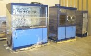
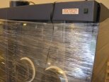
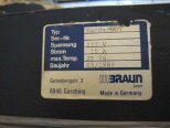
Used AIXTRON 200 #146468 for sale
URL successfully copied!
Tap to zoom




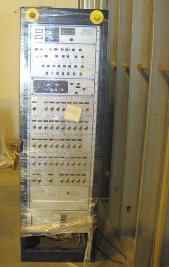

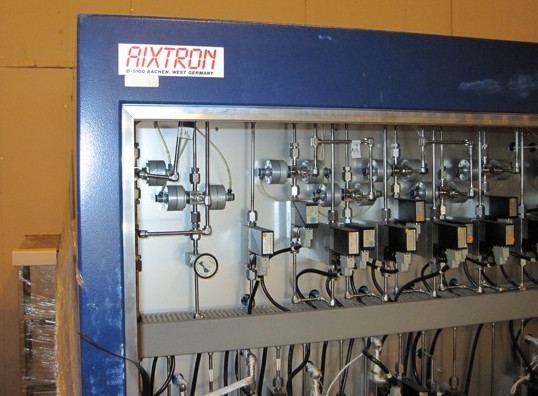


ID: 146468
Wafer Size: 2"
Vintage: 1989
MOCVD Mixed bed reactor, 2"
Configured for (3) 2" wafers
Process: GaN
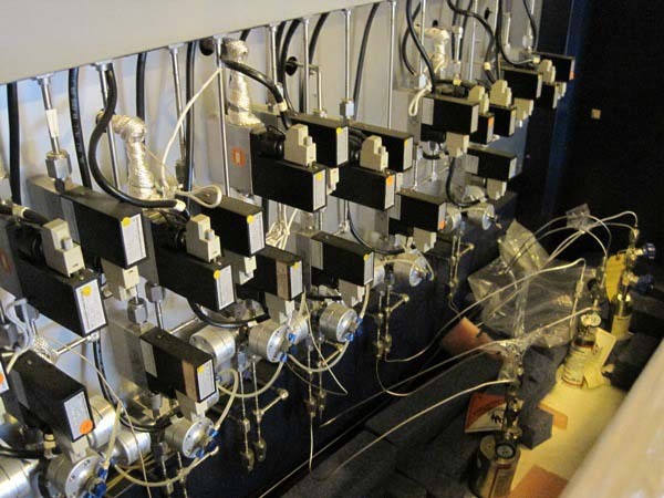
Metal organic gas bubblers included
Set up to run nitrides
1989 vintage.
AIXTRON 200 is a modern Chemical Vapour Deposition (CVD) reactor designed to grow thin films and coatings of inorganic(non-metals), and organic materials. It is capable of growing films ranging from a few atomic layers thick to greater than several microns, depending on the material and process. The reactor features two top-down, vertical furnaces with large process chambers which result in in-situ growth of thick films with excellent uniformity, thickness and step coverage over large substrates. 200 consists of two main components, the deposition chamber and the loadlock support module. The chamber has an independent heating, cooling, vent and load/unload capability with a mechanical and robotic arm. The chamber capacity is customizable to accommodate a range of multiple substrate sizes up to 200mm. It is designed with a modular concept enabling tool upgrades with ease and with the possibility of future introduction of new process gases and alternate pre-sputtering processes. The deposition chamber features two planar RF inductors with multiple RF source arms that enable a significant increase in reactive gas control in the chamber during processes like ALD, Plasma-Enhanced ALD. and PECVD. The top-down dual-chamber chamber design and process modalities like Doherty etching, crystal growth, rapid thermal processing and coating, ensures excellent uniformity and reproducibility of thin film growth or coating. The deposition chamber is equipped with a charged particle gun with an adjustable DC power supply. This type of gun is well suited for materials with an intrinsic negative charging such as polysilicon, poly-SiGe, and poly-III-V compounds. AIXTRON 200 is also equipped with a wide range of process detection and control options such as a loadlock optical emission equipment, video inspection systems, gas flow control, in-situ ellipsometry and quartz crystal microbalance. The loadlock support module includes a computer controlled wafer transfer system, vacuum and penning pumps, a computer-controlled gas abatement unit to equip the reactor with the capability to process hazardous gases, and an RF etch machine. All components are designed to comply with the ATEX certification and UVCE certification. This reactor is capable of running wide range of deposition processes such as MOCVD, ALD, PECVD, and rapid thermal processing. With high-level process control and uniformity of thin films, 200 is suitable for the fabrication of various thin film devices including thin film solar cells, LEDs, transistors, thin film batteries, and ultra-thin gate stack structures for advanced MEMS devices.
There are no reviews yet
