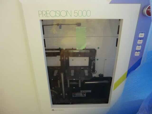
Used AMAT / APPLIED MATERIAL P5000 #293610477 for sale
It looks like this item has already been sold. Check similar products below or contact us and our experienced team will find it for you.
Tap to zoom


Sold
The Applied Materials AMAT / APPLIED MATERIAL P5000 Photoresist Reactor is a tool used in the fabrication of semiconductor wafers. It is designed to etch semiconductor substrates and coat them with photoresist layers. AMAT P5000 is a chemical vapor deposition (CVD) process tool, used in the production of integrated circuits and other microelectronic devices. APPLIED MATERIAL P5000 is composed of an outer chamber, the Process Chamber, a Gas Delivery System, a Control Unit, and a Vacuum Source, which are all enclosed in the chamber. The outer chamber is designed to be hermetically sealed, allowing it to be temperature, gas, and pressure controlled. The Process Chamber is constructed with a stainless steel chamber and a body made of quartz. The quartz helps to ensure that the necessary heat is evenly heat resistance throughout the process. The Gas Delivery System consists of two main components, a carrier gas and reactant gas. The carrier gas is used to dissolve the reactant gas in order to deposit it into the chamber. The reactant gas is then deposited into the chamber, forming the photoresist layer on the substrate. The Control Unit is responsible for controlling the pressure, gas flow, temperature, and time settings. The Vacuum Source is necessary for evacuating the Process Chamber. It is used to create a vacuum in order to establish the necessary conditions for the deposition process. It can be adjusted to a specific vacuum, typically ranging from 10-1 mbar. In order to initiate the deposition process, the substrate is transferred into the Process Chamber and a vacuum is then created. The reactant gas is then dissolved into the carrier gas and is injected into the Process Chamber. The temperature, gas flow, pressure, and time settings are then adjusted and the process is initiated. As the deposition process is carried out, a photoresist layer is formed on the substrate, creating the desired features. The Applied Materials P5000 satisfies the needs and requirements of the semiconductor industry. It is a technological advancement in the photoresist deposition process and provides greater precision and accuracy. AMAT / APPLIED MATERIAL P5000 is versatile and easy to use, allowing it to be used in a variety of situations and perform a wide range of tasks.
There are no reviews yet