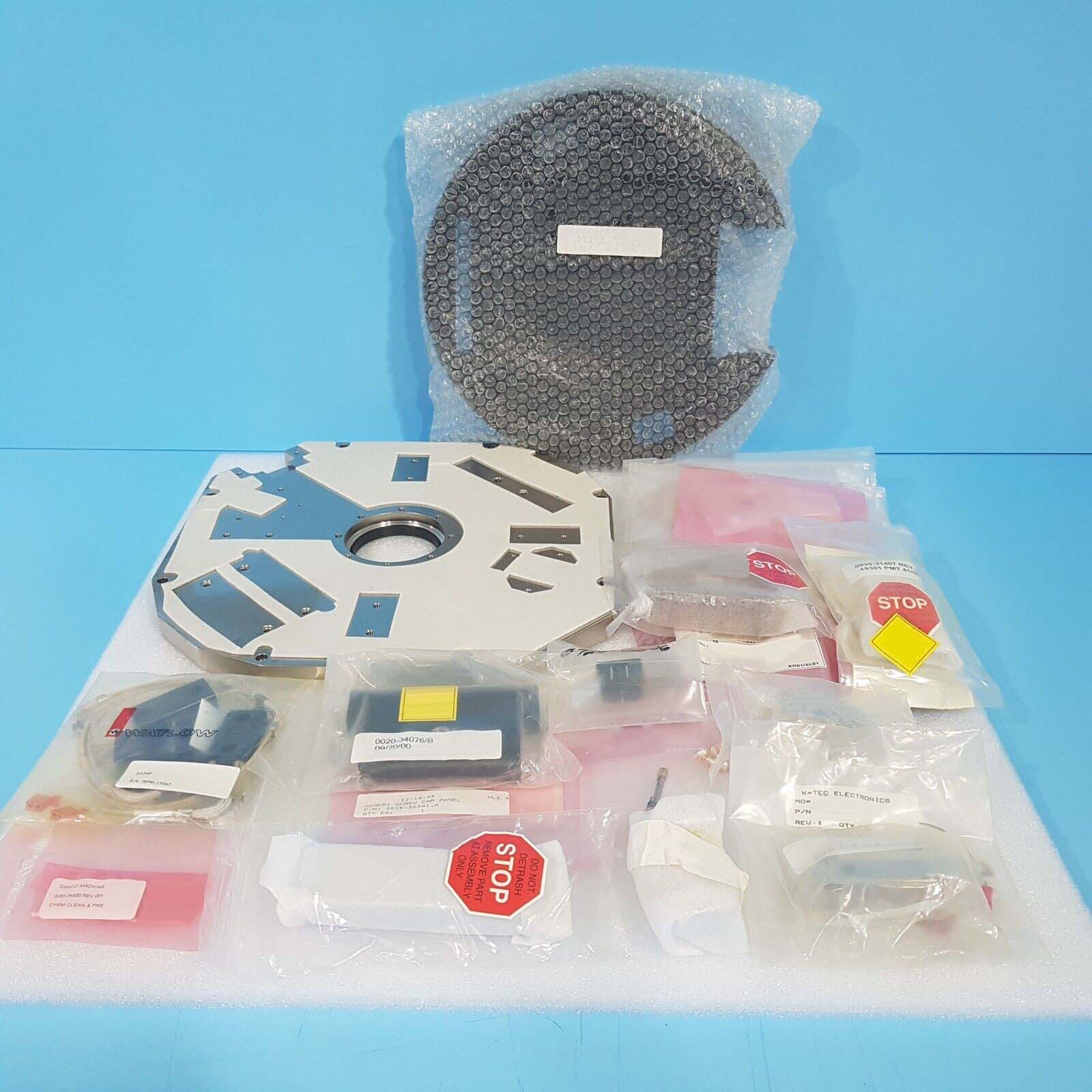
Used AMAT / APPLIED MATERIALS 0010-30319 #293661399 for sale
URL successfully copied!
Tap to zoom


AMAT / APPLIED MATERIALS 0010-30319 is a high-performance reactor equipment designed to provide superior processing and deposition capabilities for the production of compound semiconductor and related materials. This reactor is ideal for applications relating to MEMS, optoelectronic components, power electronics, and other micro- and nano-scale structures created using advanced thin film and device fabrication processes. The reactor features a large inner volume that is optimized for high-throughput processes, with maximum gas flows of up to 9000 standard cubic centimeters per minute (sccm) and total pressures up to 1000 mTorr. The reactor incorporates an RF sputter source, allowing for precise control of sputtering deposition thickness and plasma parameters, and is also equipped with an integrated rotating substrate loader, optimizing for substrate exchange and minimizing the need for extra equipment. The system is equipped with a loadlock module and the high-resolution, multi-zone digital control unit provides precise uniformity across the entire substrate. The chamber can be temperature controlled down to -20 °C, allowing for the optimization of layer thickness and composition through varying temperature ranges. The reactor utilizes a discrete quadrapole mass spectrometer with a wide range of sensitive detection capabilities, used to monitor the composition of the sputtered or deposited layers. An advanced gas delivery module also ensures precise delivery control of etching and deposition gases, with the capability to delivery up to 20 gases. The reactor machine is designed for use with a range of process tools, such as in-situ surface analysis tools, wafer handling tool, and other accessories. In addition, the asset is designed with a number of safety features, including mechanical sensors, interlocks, and venting systems. Overall, AMAT 0010-30319 reactor model delivers precise performance and unmatched throughput for advanced thin film and device fabrication processes. It is well-suited for the production of compound semiconductor materials and MEMS, optoelectronic components, and other micro- and nano-scale structures.
There are no reviews yet