Used AMAT / APPLIED MATERIALS Centura TCCP-TanOx #293757629 for sale
URL successfully copied!








Tap to zoom
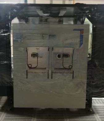

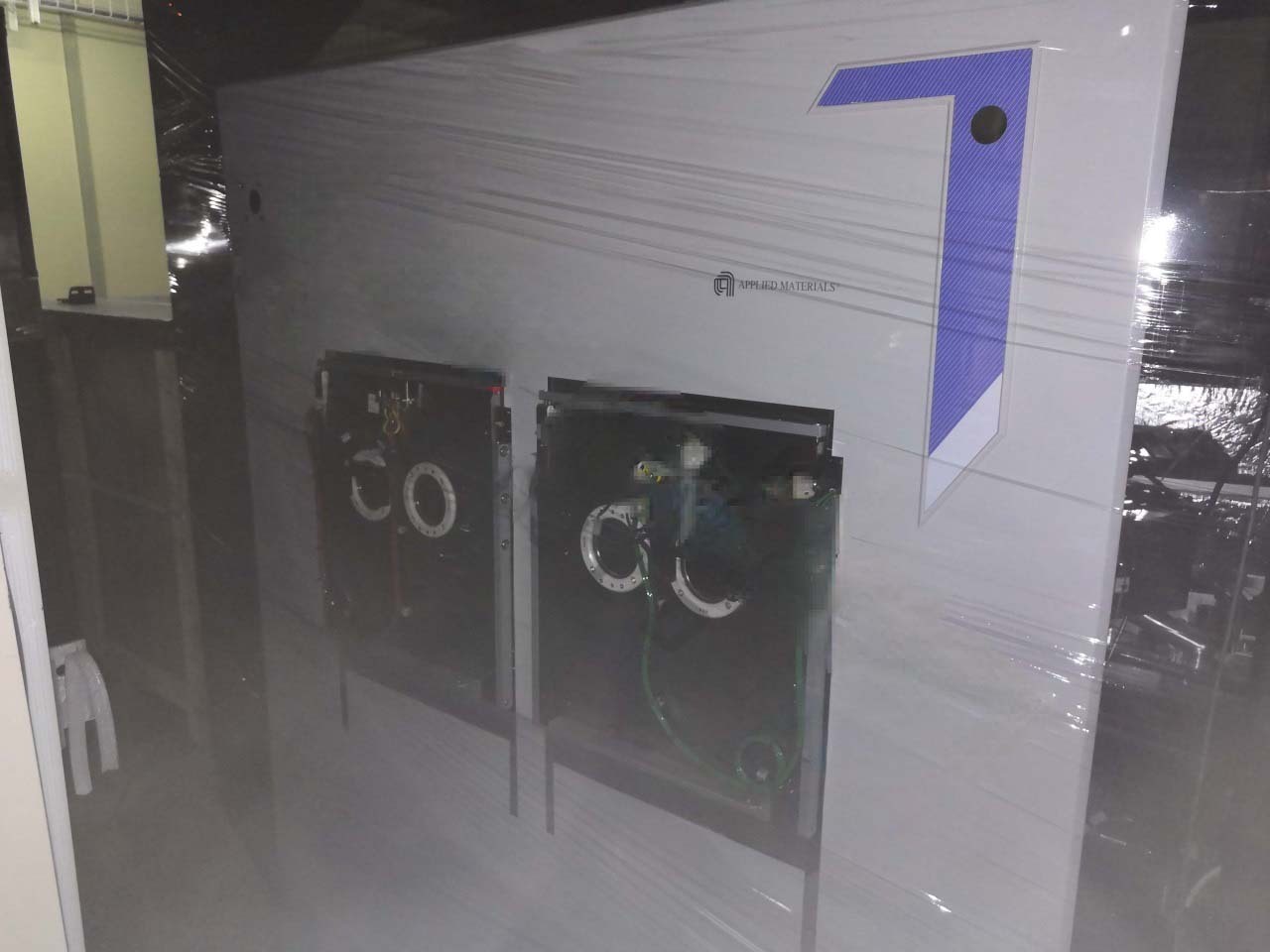
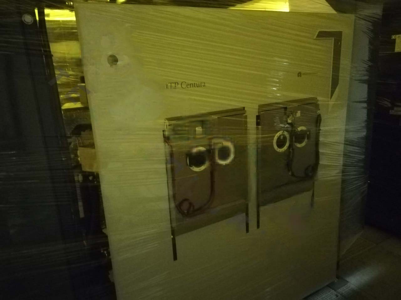
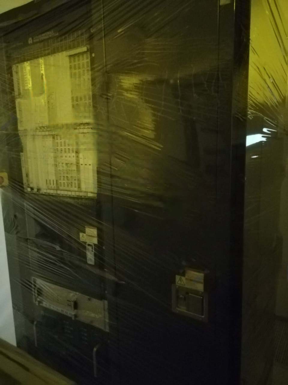
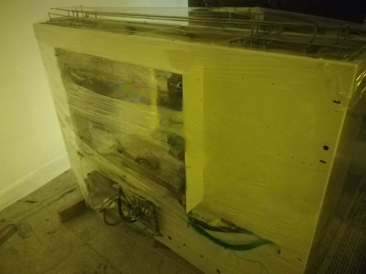
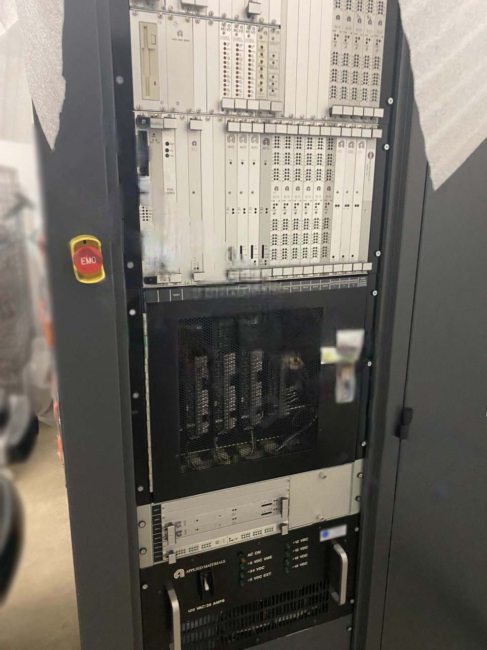
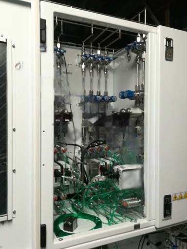
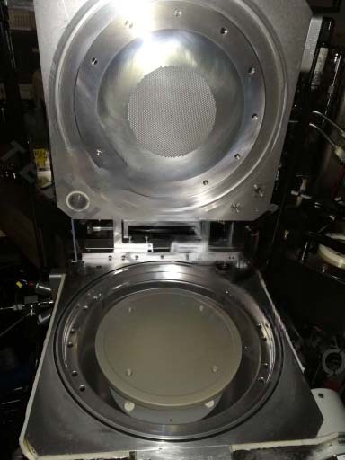
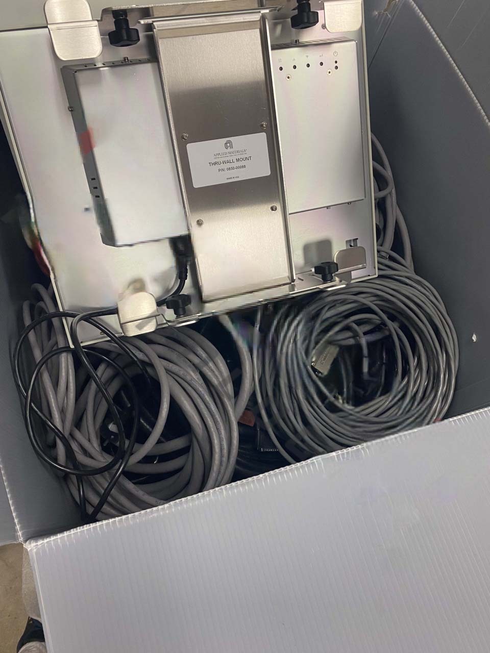
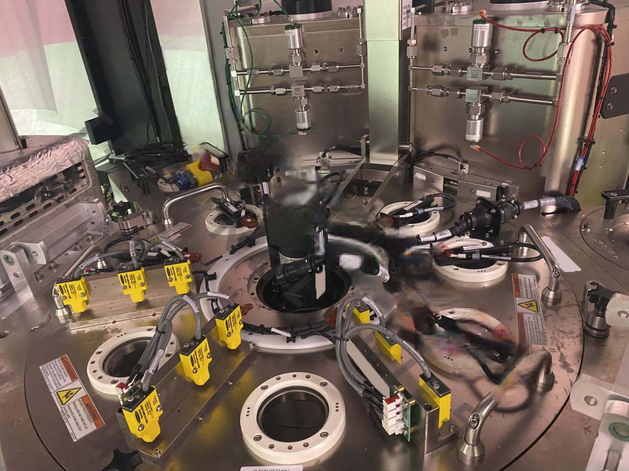
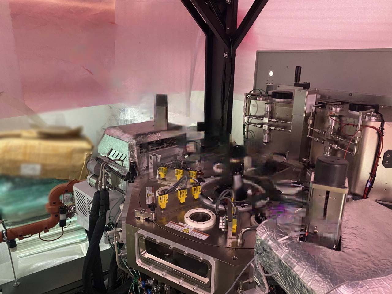
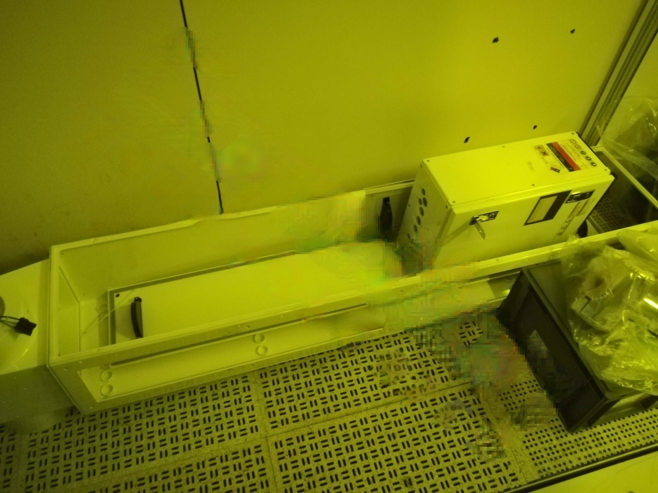
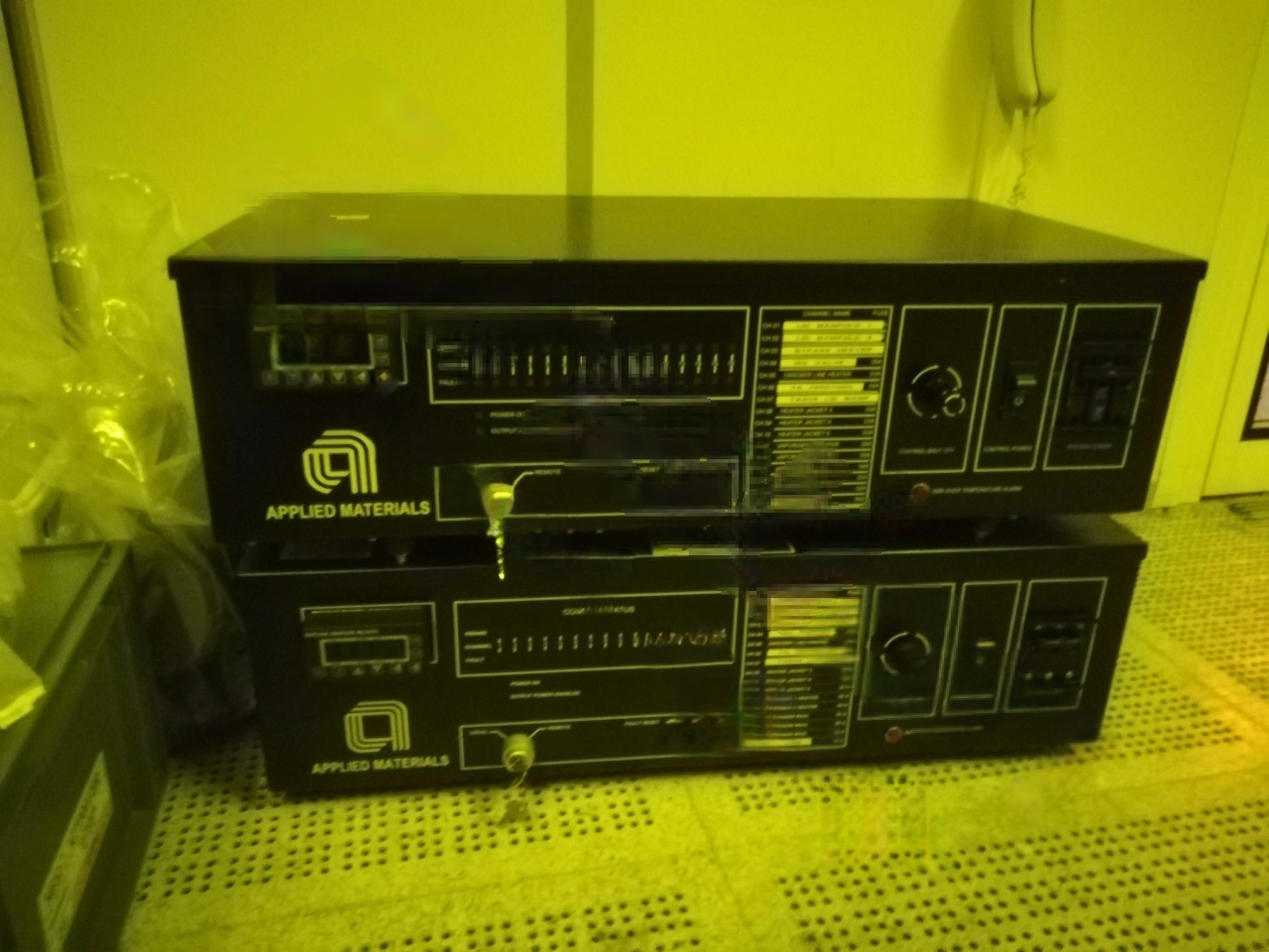
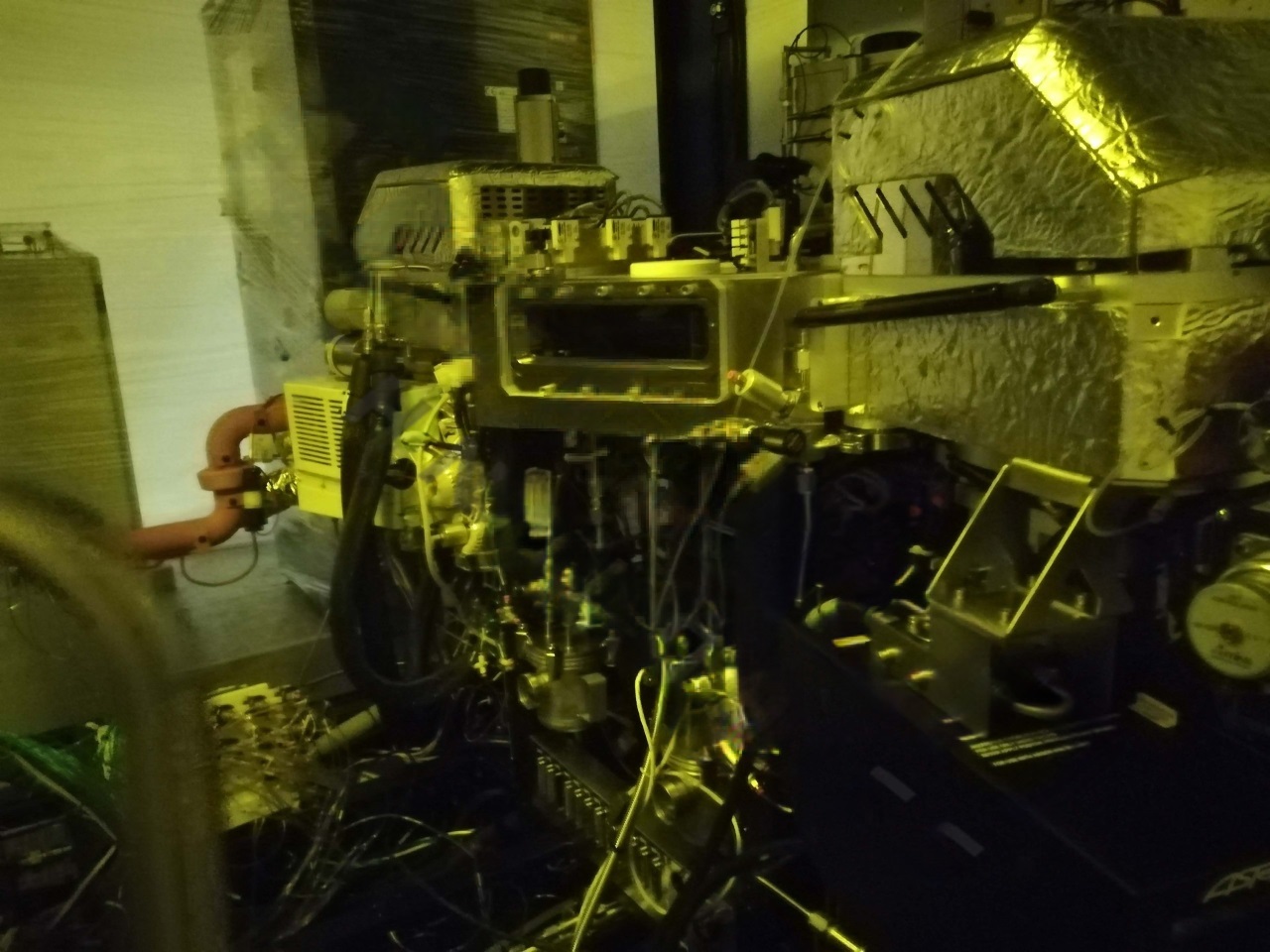
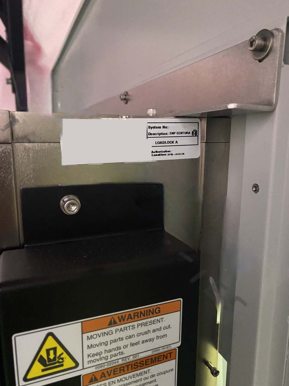
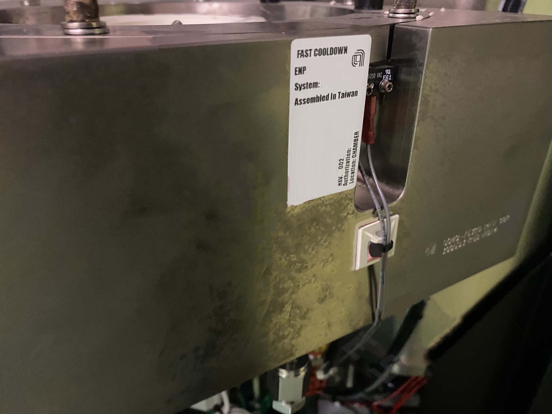
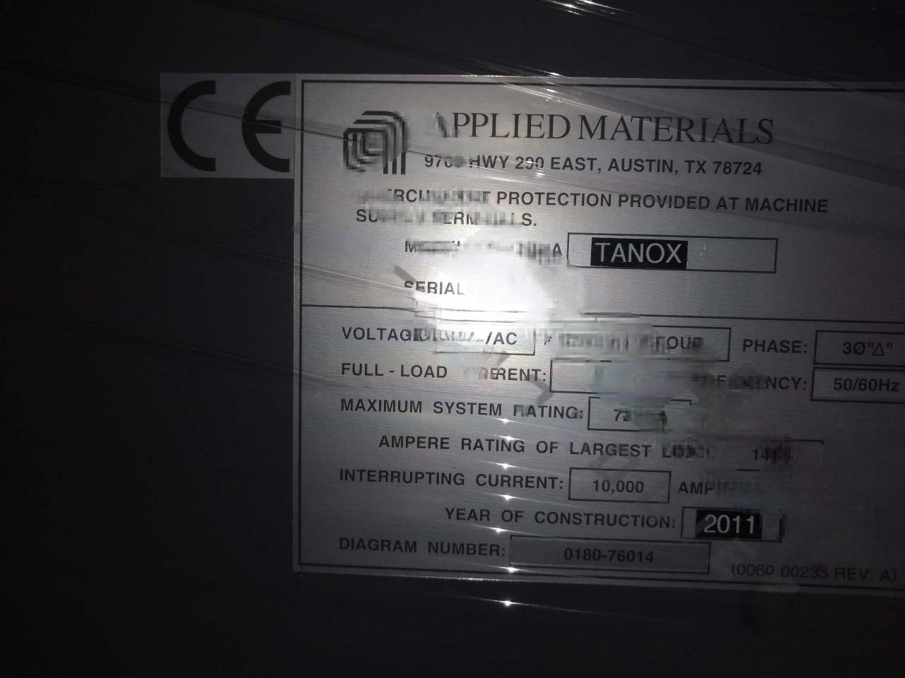
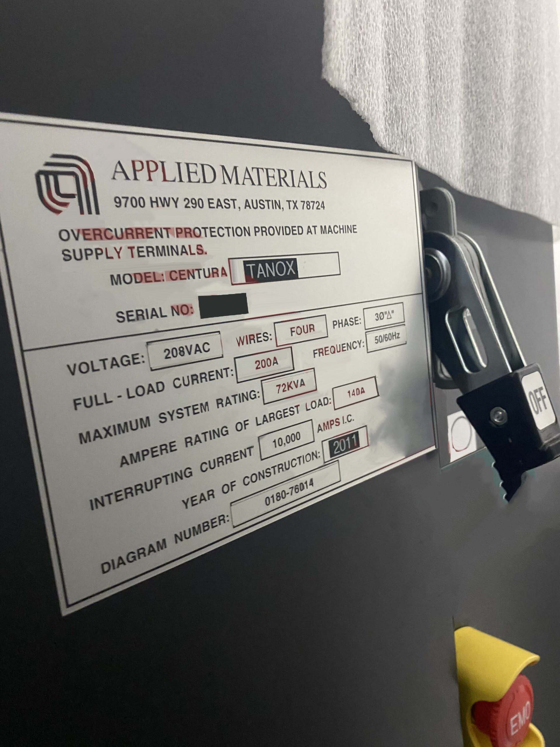
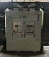
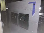
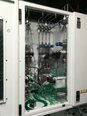
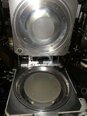
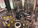
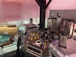
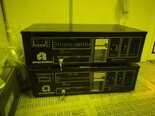
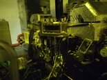
AMAT / APPLIED MATERIALS Centura TCCP-TanOx is a state-of-the-art thin film deposition reactor utilized in semiconductor manufacturing processes. This sophisticated tool offers advanced capabilities for depositing thin films with precise control over material properties, film thickness, and uniformity. AMAT Centura TCCP-TanOx reactor is specifically designed for depositing tantalum oxide (Ta2O5) thin films, a critical material used in various semiconductor applications for its dielectric properties. Key Features and Components: APPLIED MATERIALS Centura TCCP-TanOx reactor features a high-vacuum chamber where thin film deposition takes place under controlled conditions. The equipment comprises several essential components, including: 1. Vacuum Chamber: The deposition chamber is designed to maintain a high vacuum environment essential for the deposition process. The vacuum ensures minimal contamination and enables precise control over the deposition process. 2. Gas Delivery System: The reactor is equipped with a gas delivery unit that supplies precursor gases required for the deposition of tantalum oxide thin films. Precise control over gas flow rates and mixing ratios is essential for achieving the desired film properties. 3. Substrate Holder: The reactor includes a substrate holder where the semiconductor wafers are placed for thin film deposition. The substrate holder provides precise control over temperature and rotation speed to ensure uniform film deposition on the substrates. 4. RF Plasma Source: Centura TCCP-TanOx reactor features an RF plasma source that is used to create a plasma environment in the chamber. The plasma enhances the reactivity of the precursor gases, promoting film growth and adhesion to the substrate. 5. Showerhead: A showerhead assembly is employed to introduce precursor gases into the chamber uniformly. The design of the showerhead ensures even distribution of gases across the substrate surface, resulting in uniform film thickness and quality. Process Capabilities: AMAT / APPLIED MATERIALS Centura TCCP-TanOx reactor offers a range of process capabilities that make it ideal for depositing tantalum oxide thin films with precision and reliability. Some of the key process capabilities include: 1. High Deposition Rate: The reactor can achieve high deposition rates, allowing for efficient production of tantalum oxide thin films on multiple substrates simultaneously. 2. Precise Film Thickness Control: The machine enables accurate control over film thickness, allowing engineers to tailor the film properties to meet specific requirements for semiconductor devices. 3. Uniform Film Deposition: The reactor ensures uniform deposition of tantalum oxide thin films across the entire substrate surface, eliminating variations in film thickness and quality. 4. Low Contamination: The high-vacuum environment of the reactor minimizes the presence of contaminants, ensuring high-purity tantalum oxide thin films suitable for demanding semiconductor applications. Applications: AMAT Centura TCCP-TanOx reactor is widely used in the semiconductor industry for depositing tantalum oxide thin films in various applications. Some common applications of tantalum oxide thin films include: 1. Capacitor Dielectrics: Tantalum oxide thin films are used as dielectric layers in capacitors, providing high capacitance density and excellent insulating properties. 2. Resistive Memory Devices: Tantalum oxide thin films are utilized in resistive memory devices such as ReRAM and FeRAM for their stable switching characteristics and high endurance. 3. Optical Coatings: Tantalum oxide thin films can be used as optical coatings for anti-reflective and protective purposes in optical devices. In conclusion, APPLIED MATERIALS Centura TCCP-TanOx reactor is a cutting-edge tool for depositing tantalum oxide thin films in semiconductor manufacturing. With its advanced features, precise process control, and reliable performance, the reactor plays a crucial role in enabling the production of high-quality semiconductor devices with enhanced functionality and performance.
There are no reviews yet