Used AMAT / APPLIED MATERIALS ENDURA #9105850 for sale
URL successfully copied!
Tap to zoom
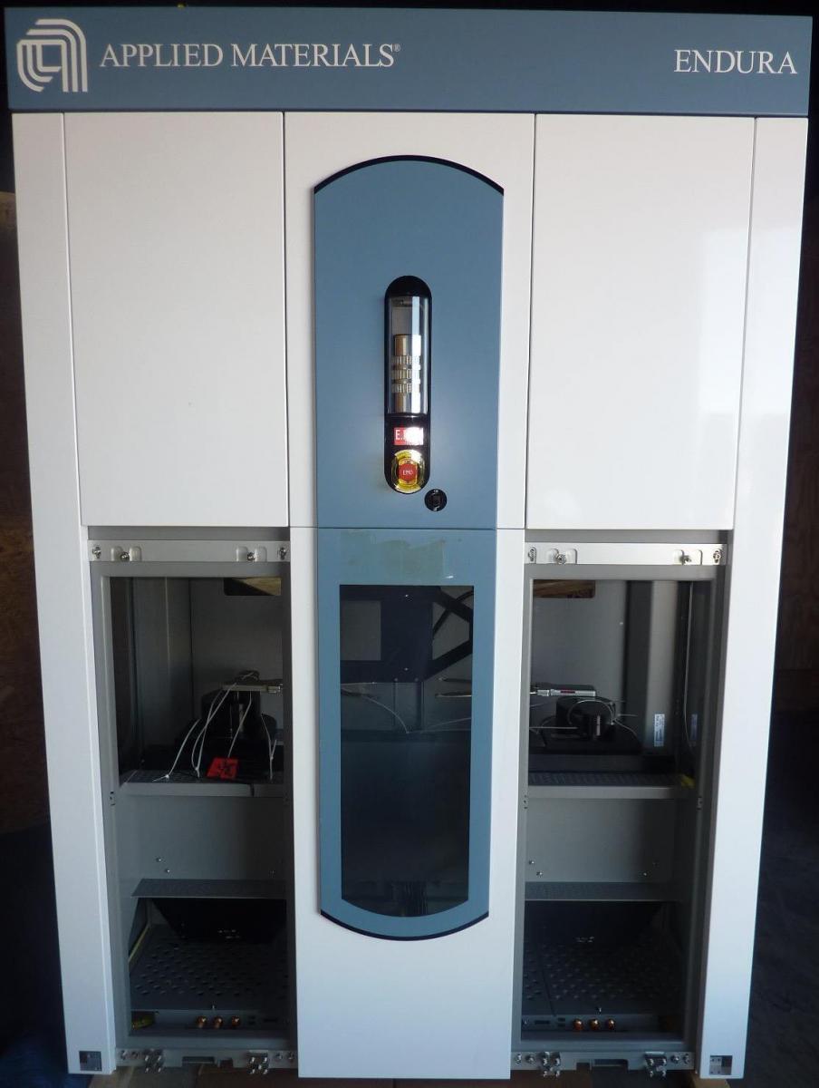

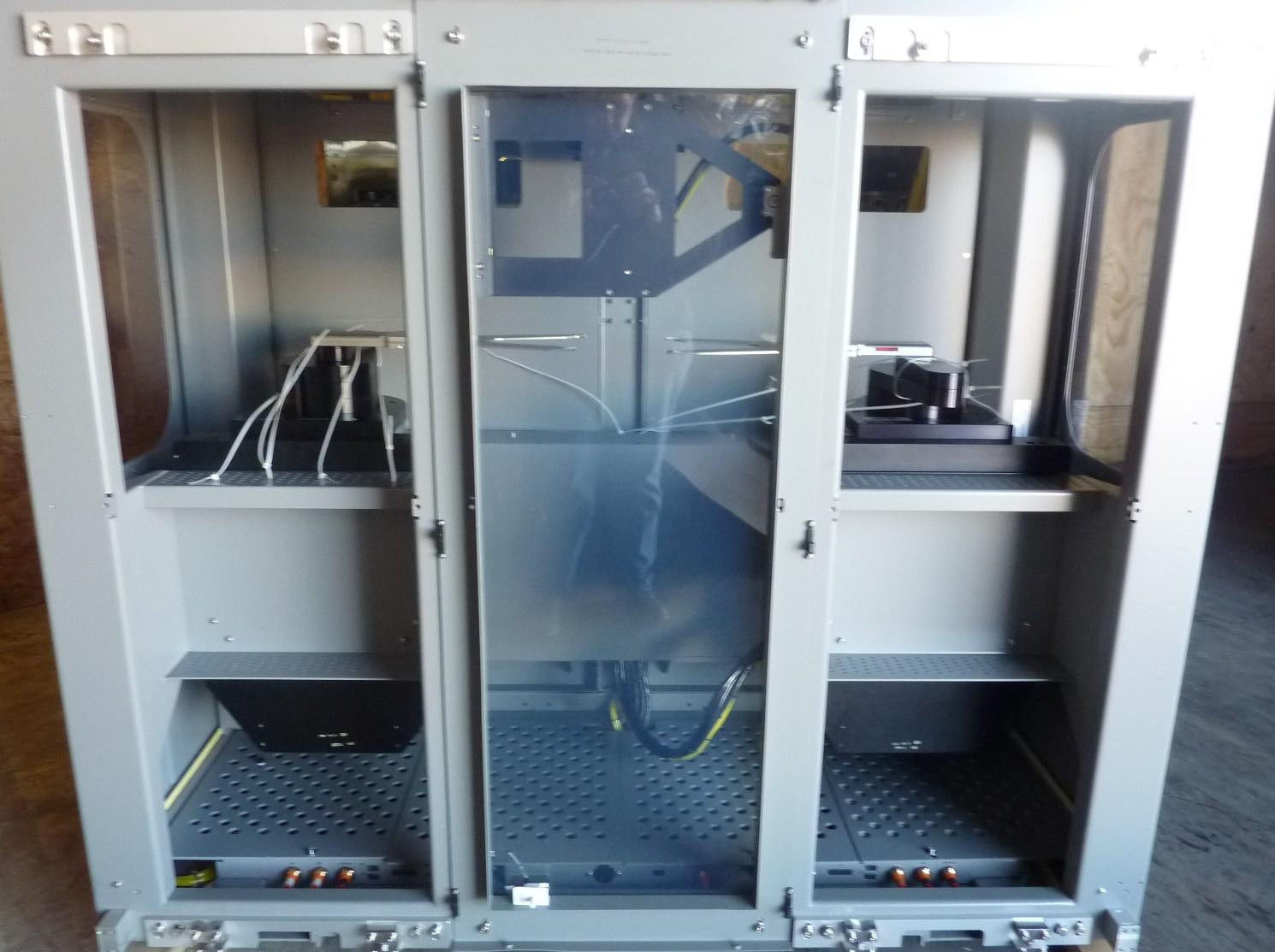











ID: 9105850
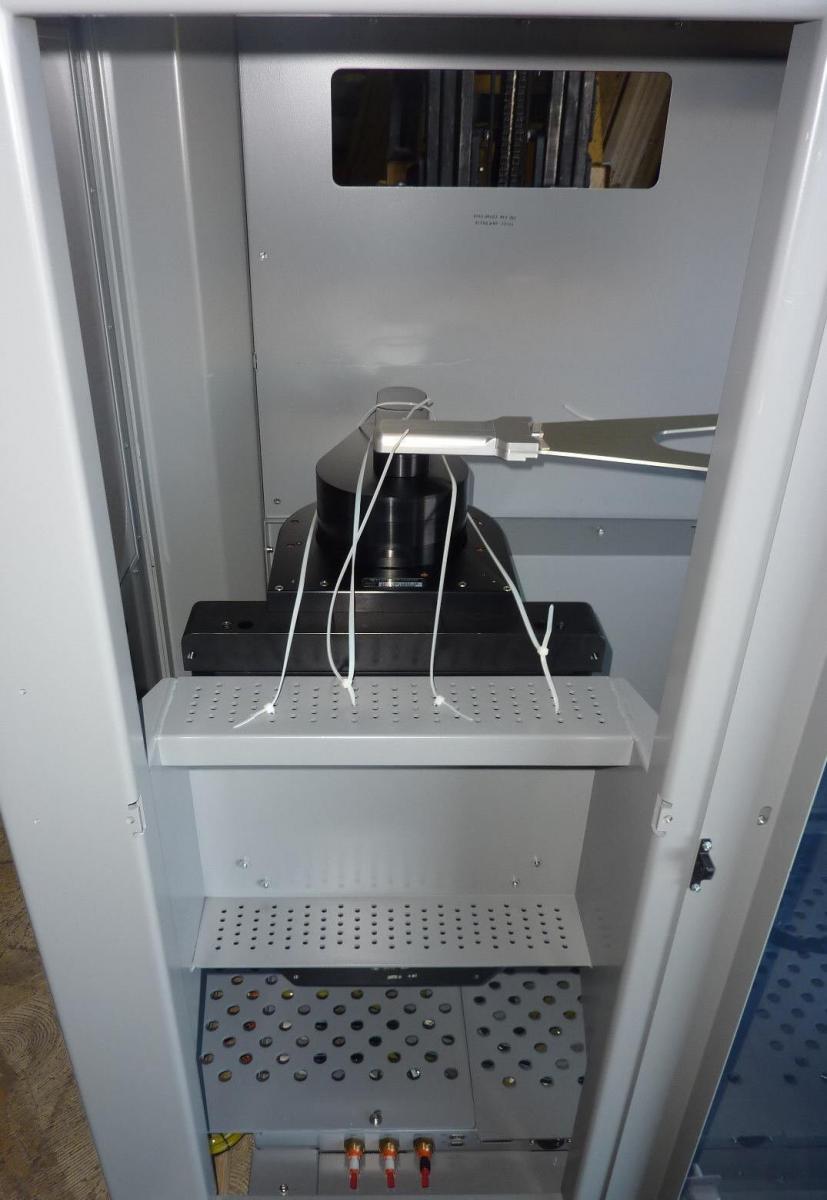
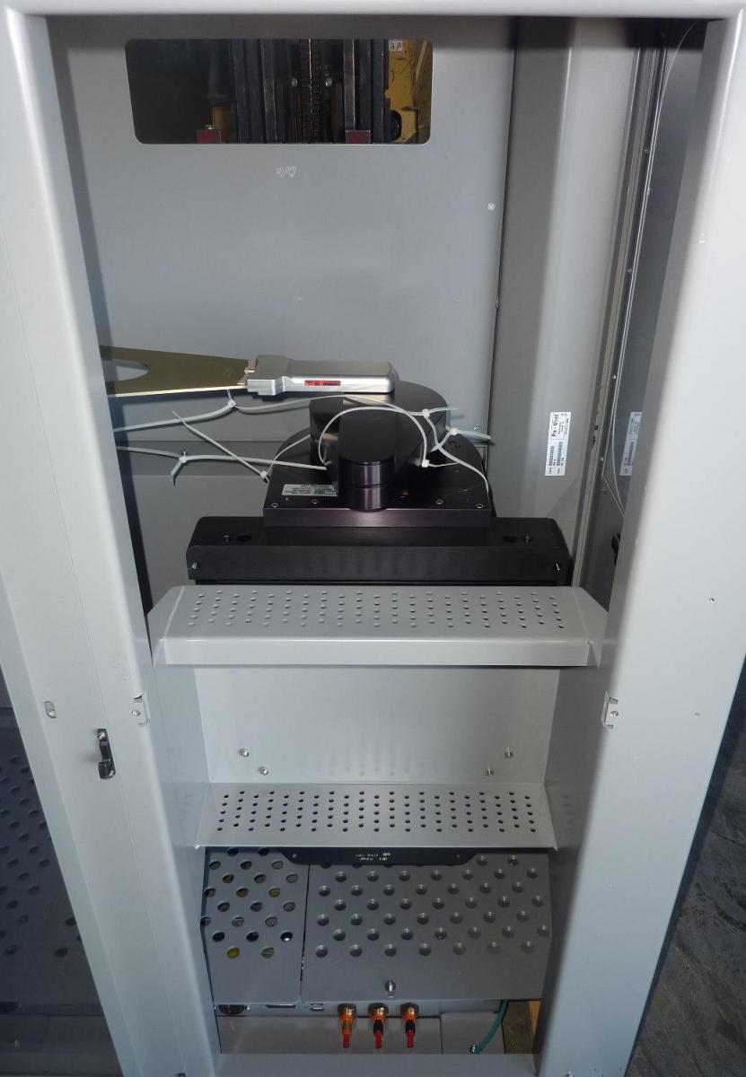
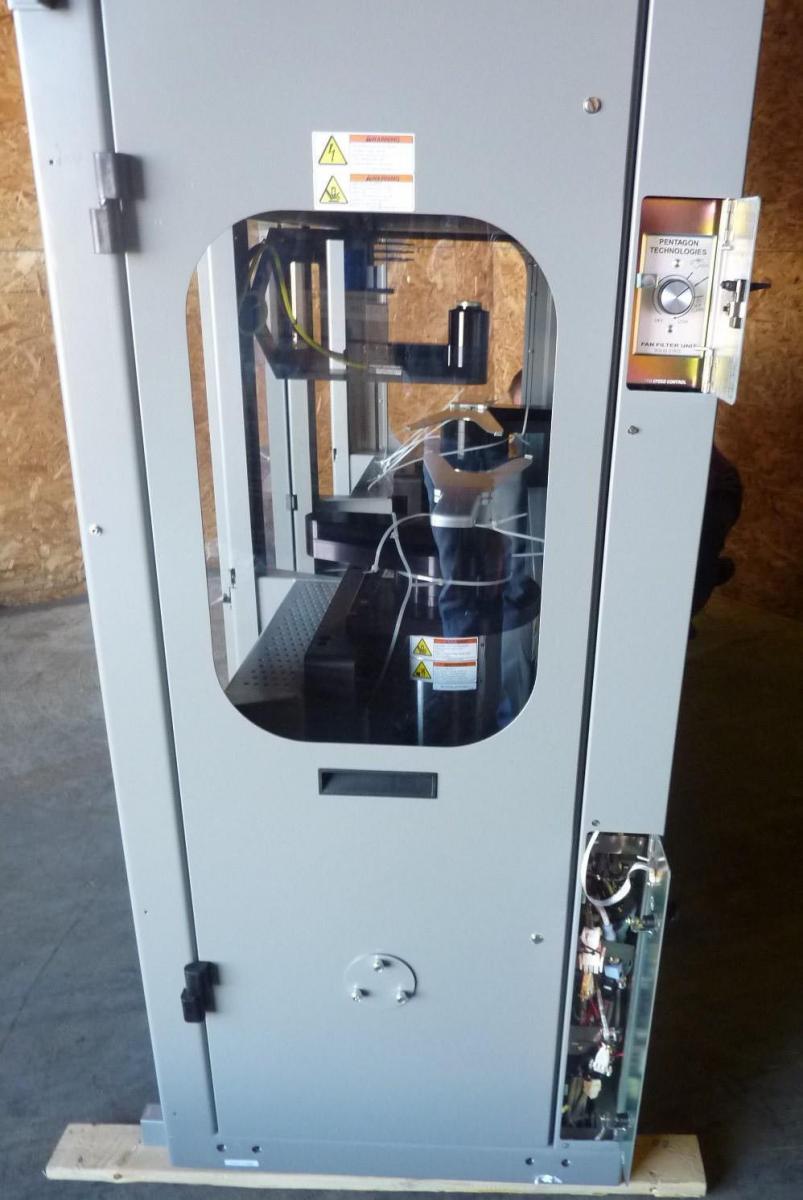
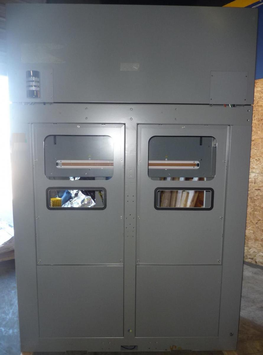
Load Port Interface, 8"
From 8" Endura CVD System
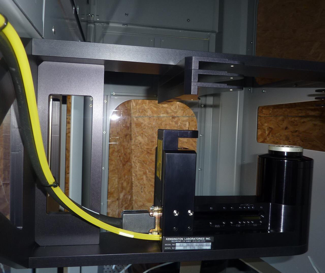
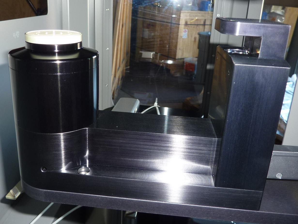
(1) Prealigner: Kensington P/N: 25-3600-0300-03
(2) Servo Controllers
Robots:
Kensington P/N: 35-3700-1425-18
Kensington P/N: 15-3702-1425-25
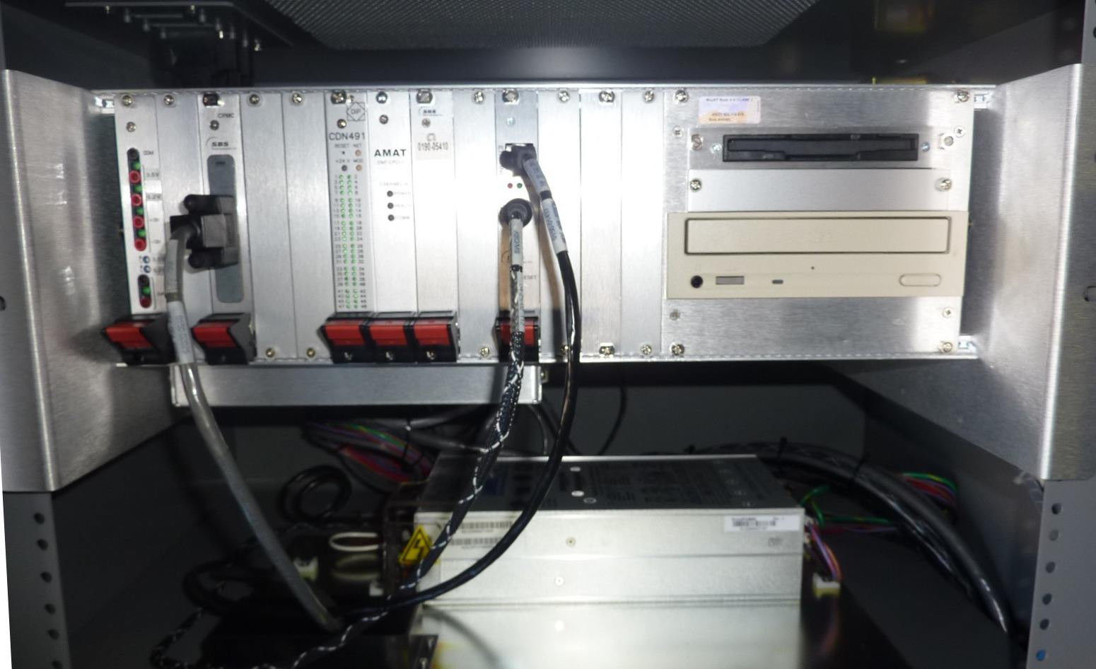
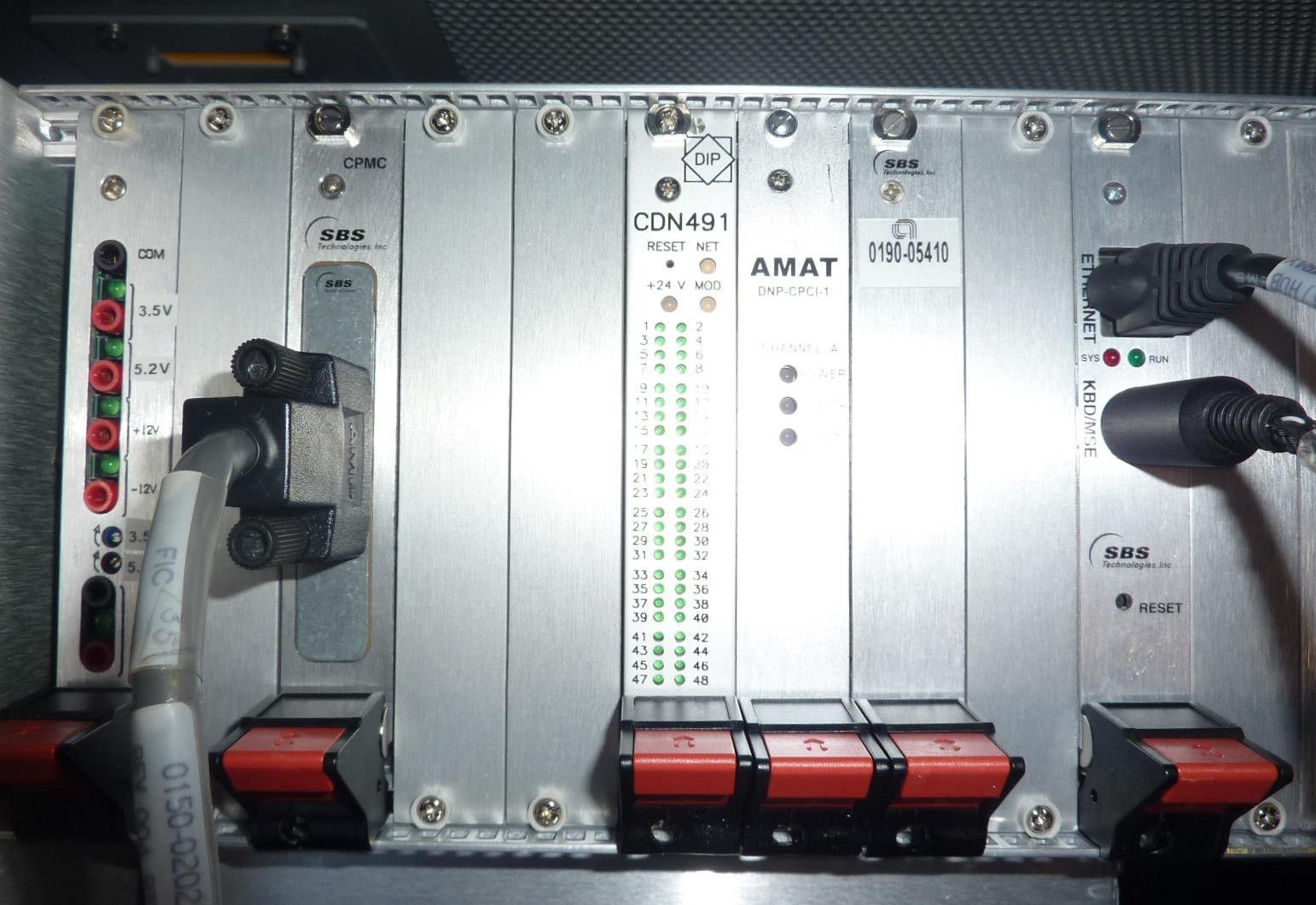
PCB's:
AMAT P/N: DNP-CPCI-1
MKS P/N: CDN491
SBS P/N: 0190-05410
SBS P/N: Single board computer
SBS P/N: CPMC.
AMAT / APPLIED MATERIALS ENDURA reactor is an industrial-grade workhorse reactor used in semiconductor manufacturing. This physical vapor deposition (PVD) tool is designed to deposit a thin film of material on wafers, chips, and other substrates for diverse applications such as circuitry, photonics, wearables, and biomedical medical implants. AMAT ENDURA reactor utilizes a patented three-chamber design that allows for multiple depositions and exposures in each sequence. It supports deposition materials such as copper, tungsten, aluminum and silicides, as well as capping materials such as titanium or aluminum. Thanks to its precision process control and repeatability, this tool delivers consistent results and mask conformality. With its ultra-low particle emissions, a particle counter is not required and there is less need for wafer reclaiming and cleaning, resulting in increased throughput over other PVD tools. APPLIED MATERIALS ENDURA reactor also features a flexible controller that allows for tuning of the chamber environment to provide optimal deposition conditions, and a pressure window for rapid pressure control. This helps to ensure that a high quality thin film is deposited. In addition to its deposition capabilities, ENDURA is capable of wet etching and surface cleaning using a variety of chemistries including hydrogen peroxide and TMAH. This etching capability helps to enhance the performance of some devices, such as MEMs and other devices sensitive to poor wet etch results. Due to its versatility, robust design, and piece of mind capability, AMAT / APPLIED MATERIALS ENDURA reactor is widely used in semiconductor and optoelectronic manufacturing. It enables fast and accurate thin film deposition, achieves excellent repeatability of process parameters, and provides good process control.
There are no reviews yet


