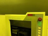
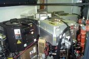
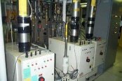
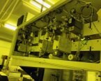
Used AMAT / APPLIED MATERIALS P5000 #9181556 for sale
URL successfully copied!
Tap to zoom
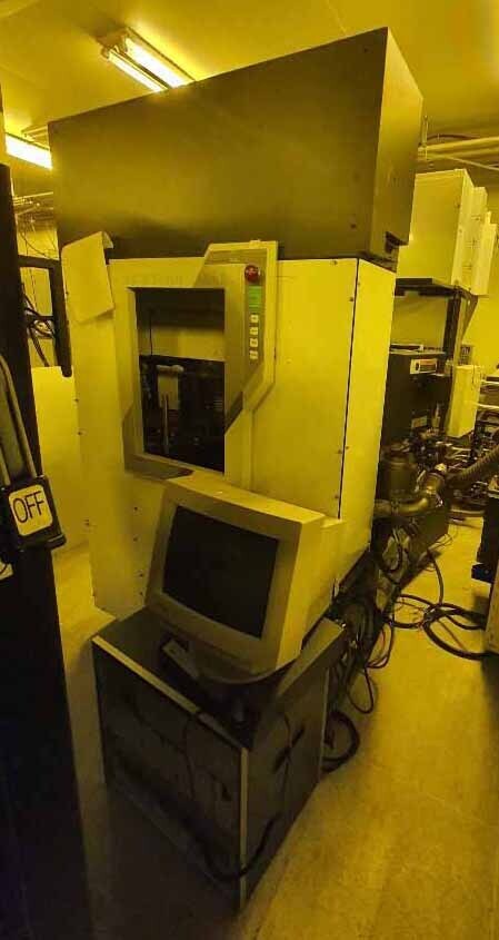

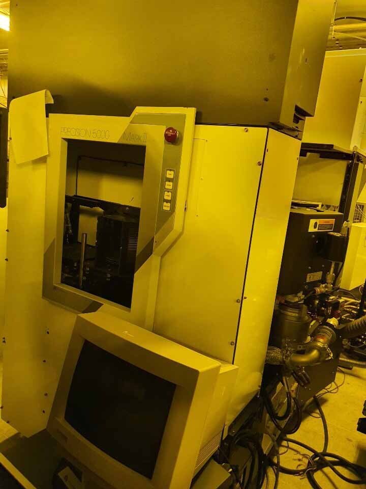


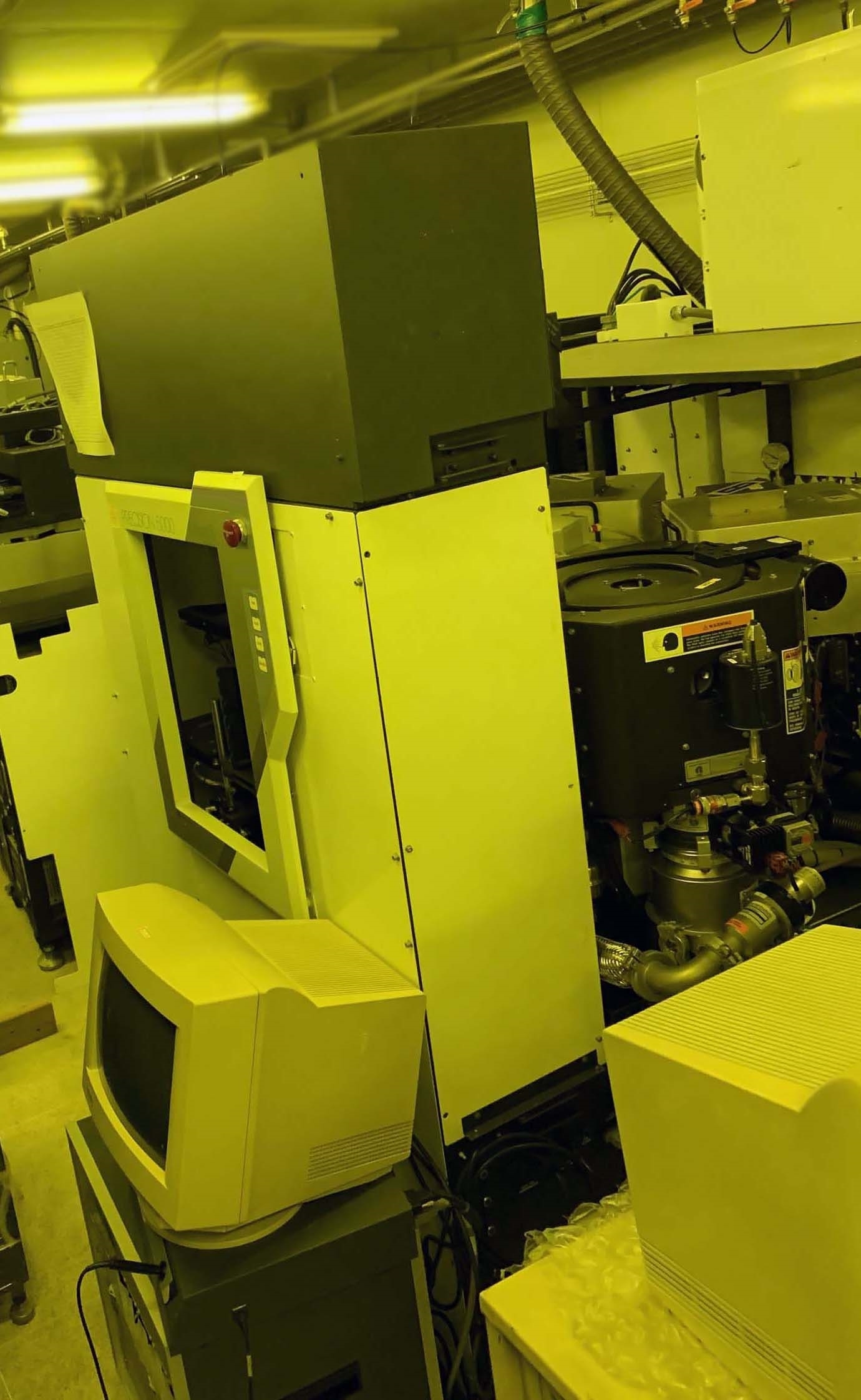



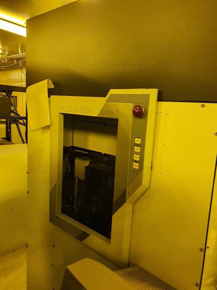

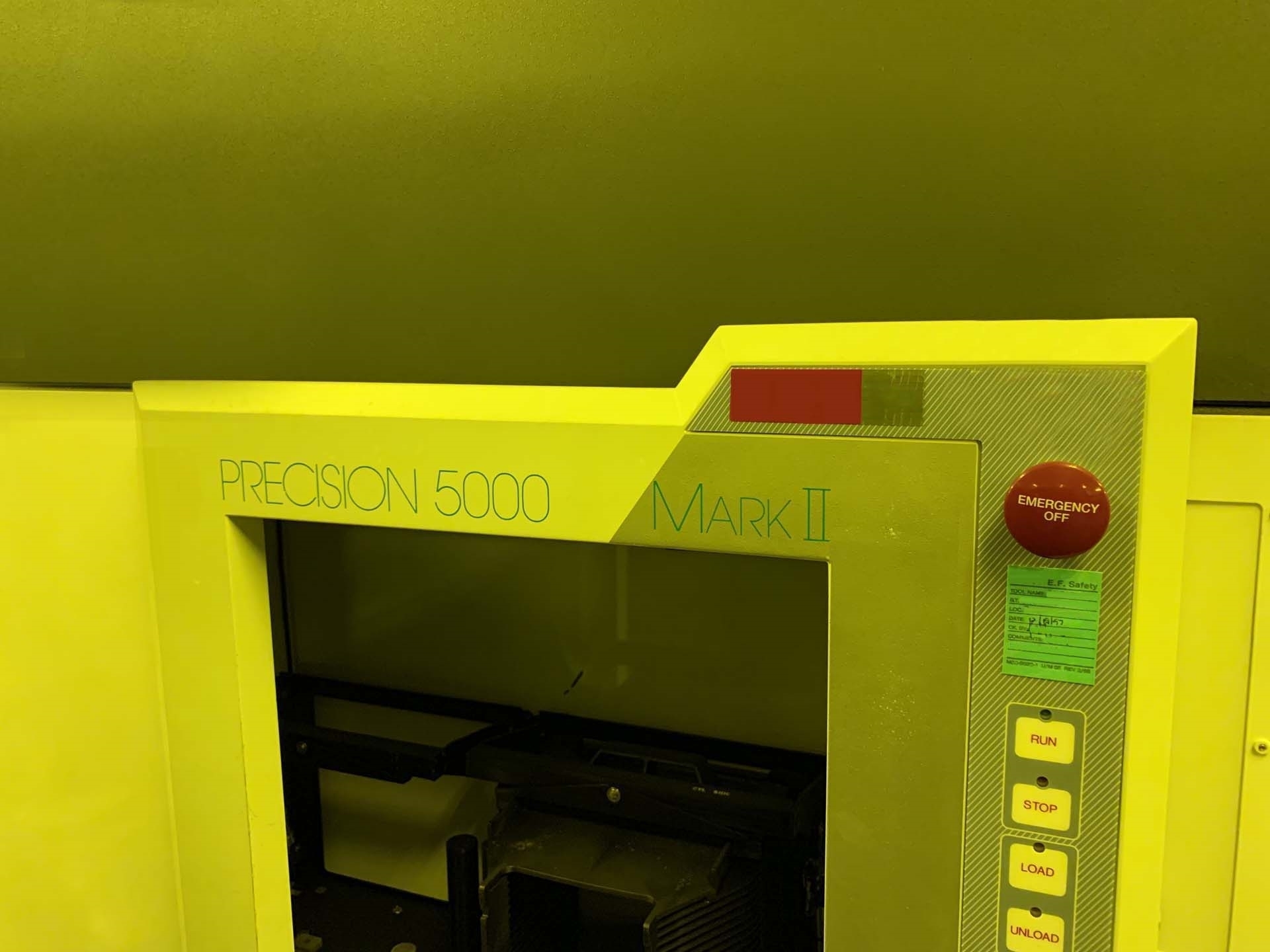

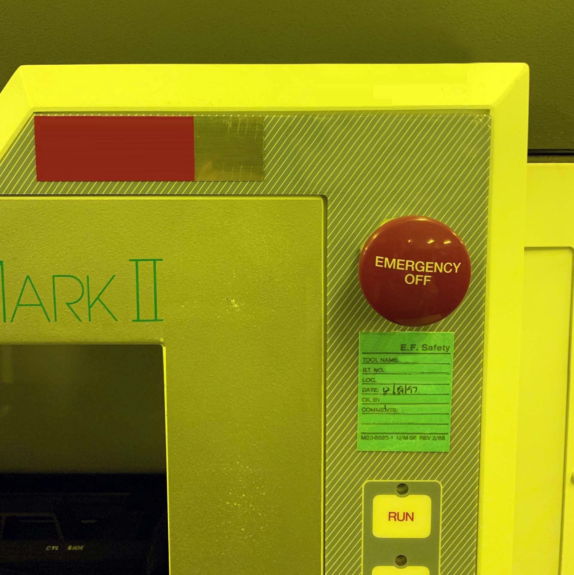

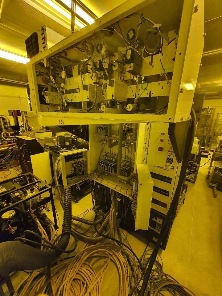






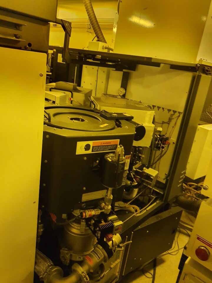

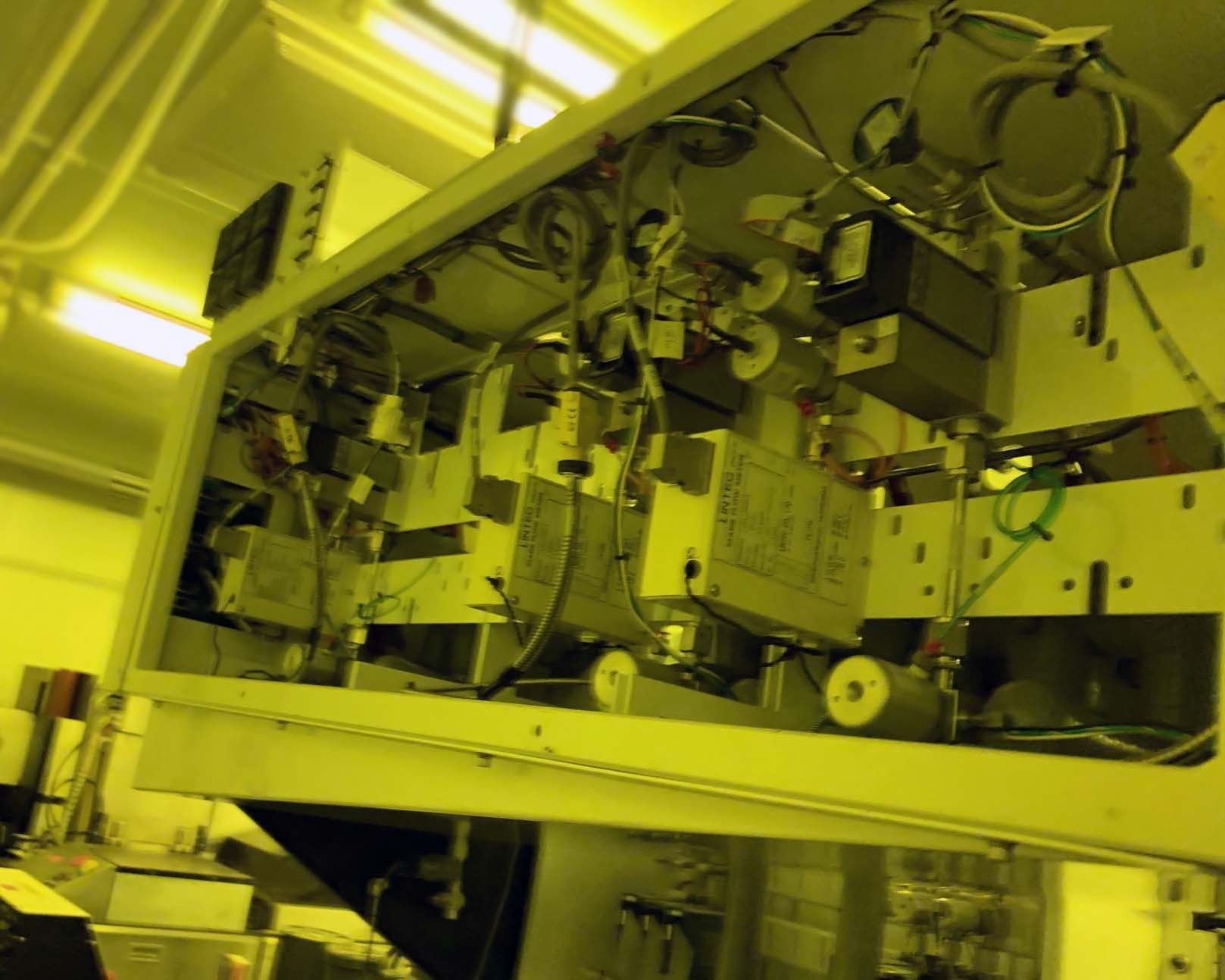

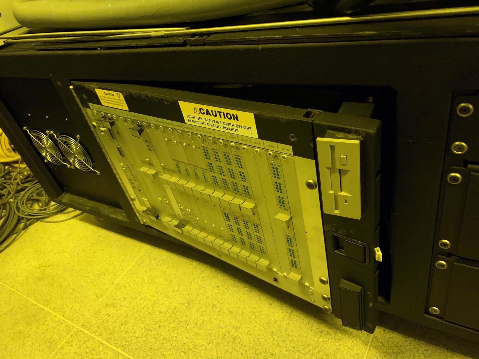


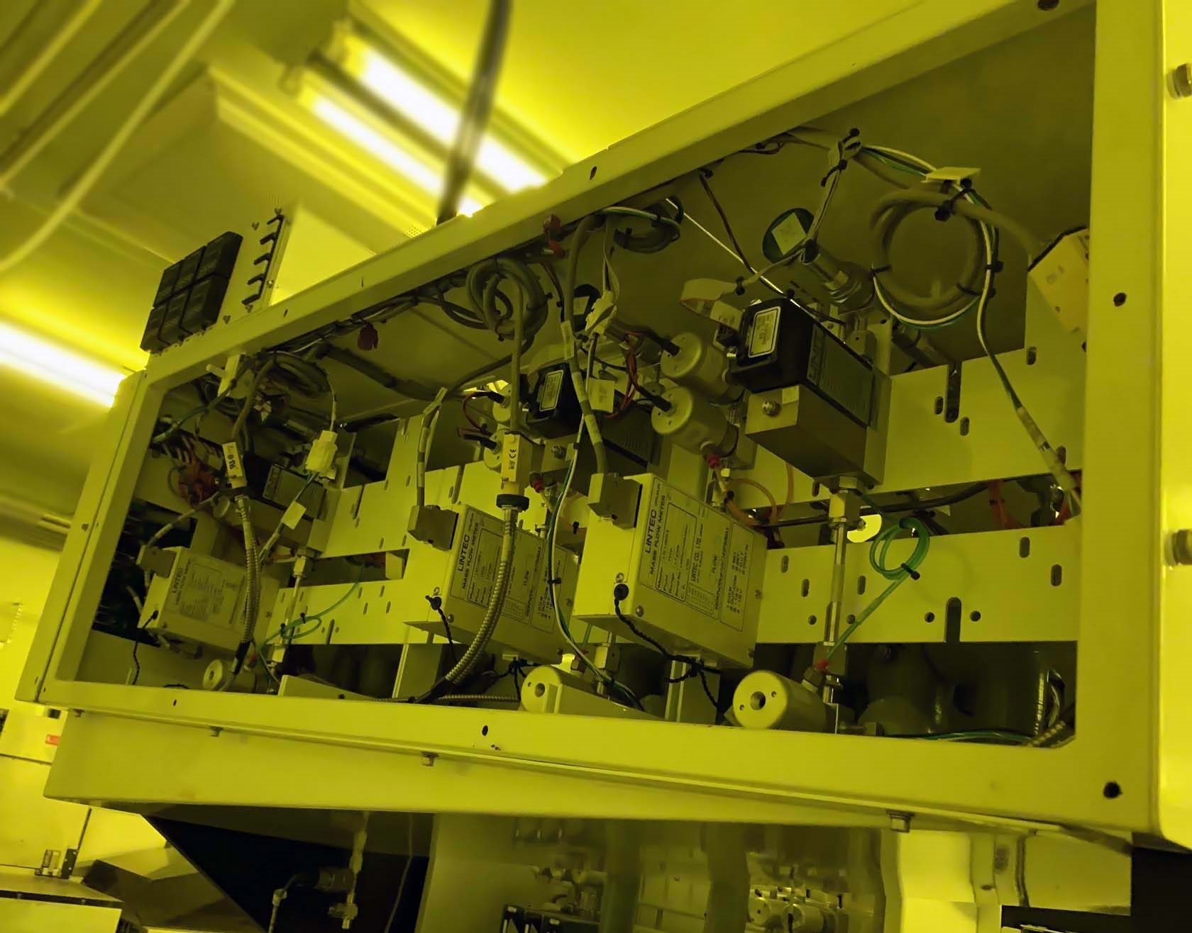






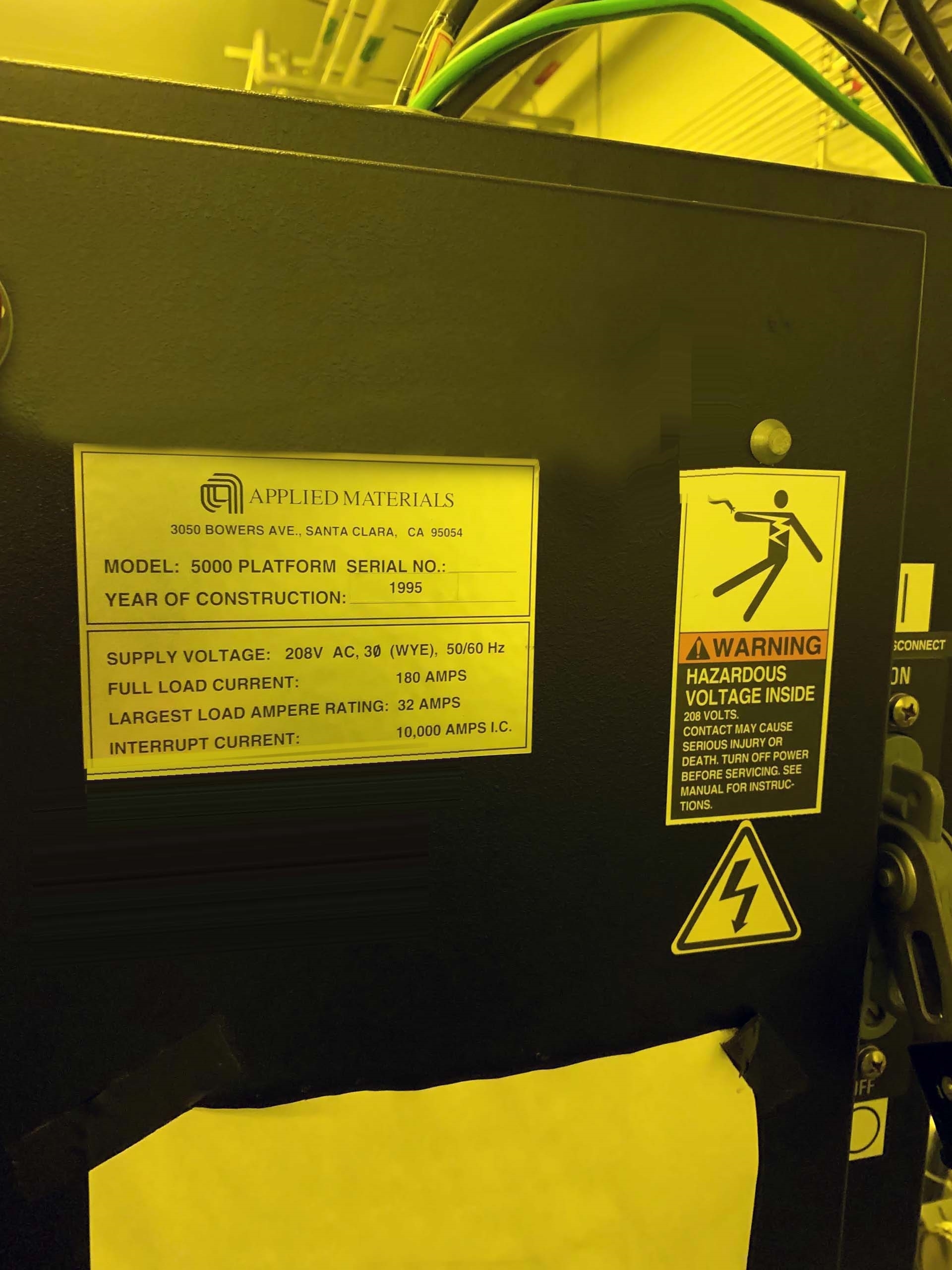

ID: 9181556
Wafer Size: 8"
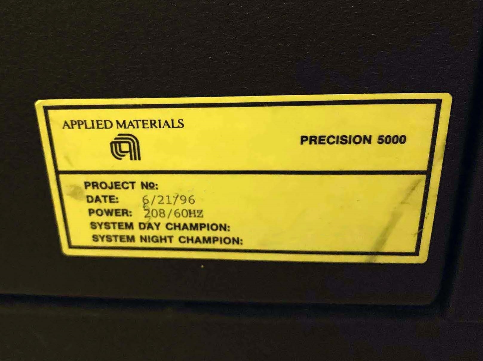
Vintage: 1995
TEOS CVD Systems, 8"
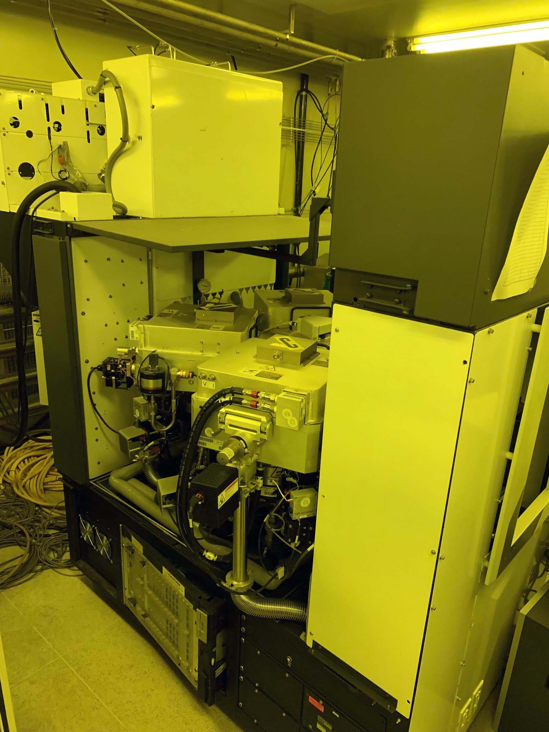
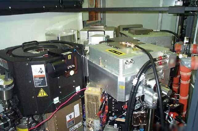
(3) Deposition Precision Liquid Injection System (PLIS) chamber
Sputter etch chamber
Parts / Modules:
DELATECH 859 Scrubber
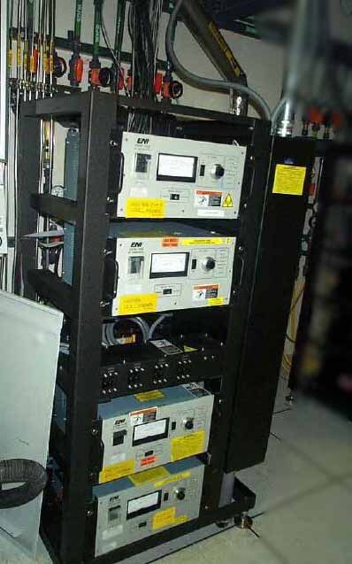
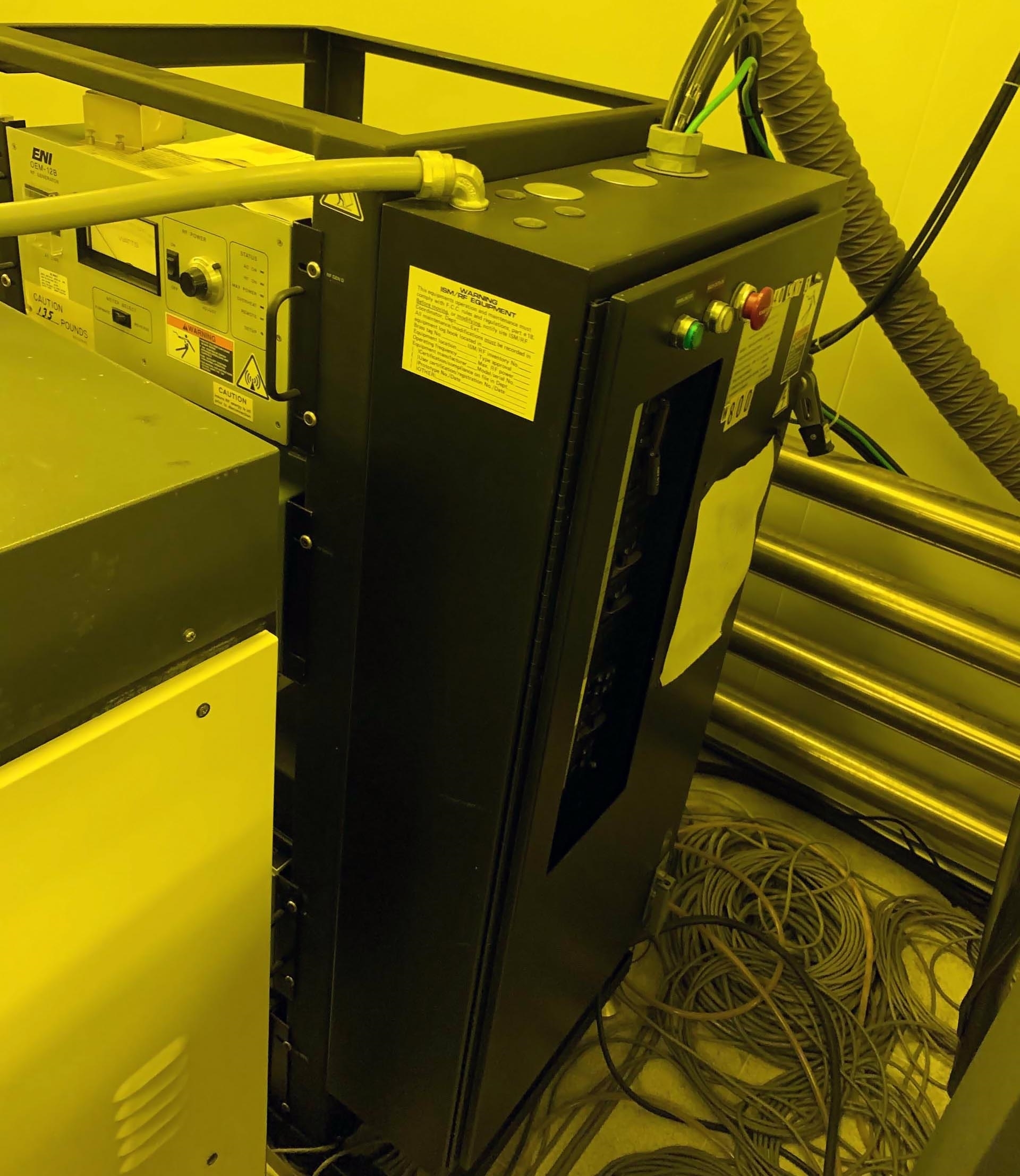
Main power box with (4) ENI RF generators
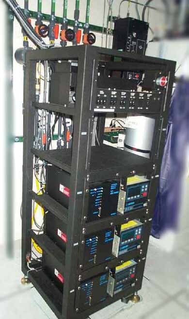
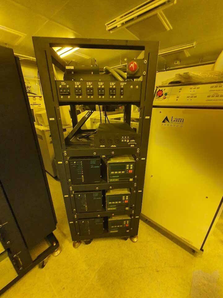
DELTA RF Generator rack with (3) RFPP generators
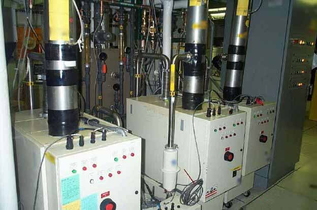
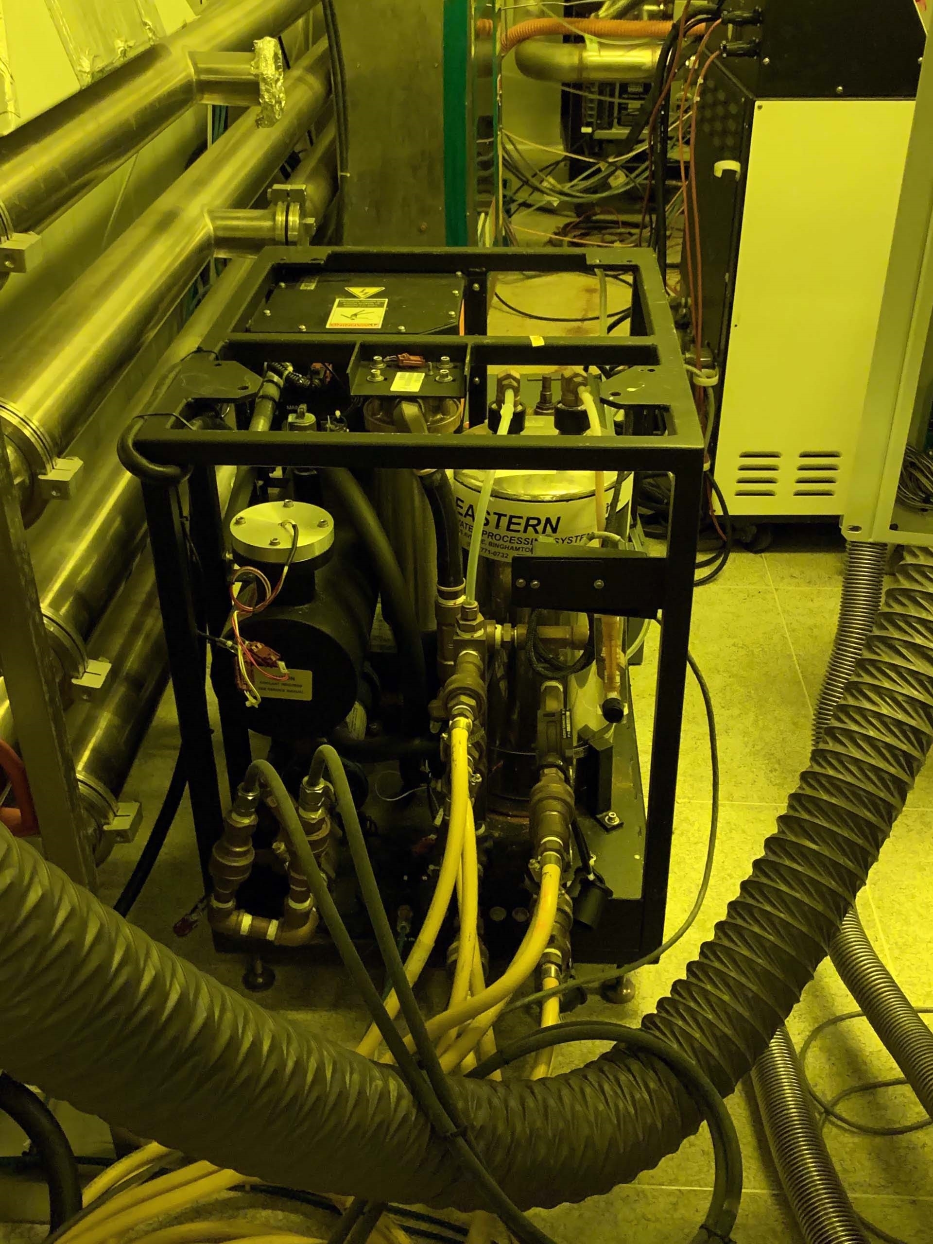
APPLIED MATERIALS '0' Heat exchanger
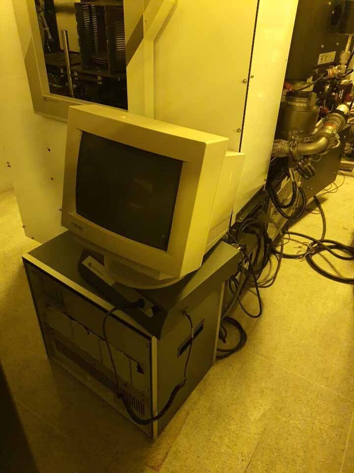
Front and rear monitor
(3) EBARA Pumps: 50x20
(2) EBARA Pumps: 40x20
Mini controller
1995 vintage.
AMAT / APPLIED MATERIALS P5000 is a type of reactor designed and released by the software and hardware manufacturer AMAT, Inc. AMAT P-5000 is a tool used by chip makers to perform high-quality photolithography processes. It utilizes mask exposure and deposition processes to create precise patterns on a substrate surface. APPLIED MATERIALS P 5000 is a high-powered, fully automated machine, powered by a 500 watt discharge lamp and featuring a recipe-controlled wafer transport system. AMAT / APPLIED MATERIALS P-5000's intelligent design enables users to easily switch between 10 different photoresist processes, including lithography and etching. AMAT P5000 is capable of producing patterns as small as 50 nanometers in diameter. It also offers both manual and automatic exposure, as well as a function that allows users to select lithography exposure pathways. P 5000 is well known for its efficient and reliable performance, as well as its intuitive user interface. Its main components include a robot arm, exposure platform, control modules, and quartz exposure vessels. The robot arm ensures accurate placement of substrates and masks into the exposure chamber. The exposure platform offers variable aperture sizes for precise patterning when used with a mask. The control modules allow for precise exposure control, focusing and wafer transport speed adjustments. Lastly, the quartz exposure vessels are designed to be impervious to chemical and thermal effects during operation. AMAT P 5000 is an excellent choice for chip makers that need precise and reliable exposure for their tools. Its features and flexibility enable users to perform a range of photolithography operations quickly and accurately. Its robust design makes it a reliable solution for up to 300mm wafers, offering a high level of flexibility for chip makers that require precise, repeatable patterning processes. Lastly, its user-friendly interface and compatibility with existing software and hardware systems make it easy to incorporate into production environments.
There are no reviews yet


