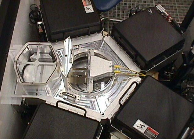
Used APPLIED MATERIALS P 5000 #163405 for sale
It looks like this item has already been sold. Check similar products below or contact us and our experienced team will find it for you.
Tap to zoom


Sold
ID: 163405
Wafer Size: 8"
PECVD system, 8"
Configuration: (4) CVD chambers
Process gases: Silane, Ammonia, Nitrous Oxide, Nitrogen Trifluoride
Precision 5000 Mark II Mainframe
Precision 5000 Software Version 5.03 (Year 2000 Compliant)
SECS Communication Port
Laminar flow mini-environment behind input/output window
Mark II ZA (zero adjust) actuators and gates for process chambers
Process chamber configured for ceramic chuck operation
15 slot storage elevator for faster run rates
eDOC remote system for combustion of un-reacted silane
Nitride thin film configured (no hotbox)
Heat exchanger
Remote frame with remote AC power box
(1) High frequency RF generator per chamber on remote frame
(4) BOC-Edwards iQDP40/iQMB250 pumps/blowers for dep chambers
BOC-Edwards iQDP80 pump for loadlock
Ergonomic Cassette Load/Unload
Excursion Prevention (EP) software ready
Currently crated.
APPLIED MATERIALS P 5000 reactor is a state-of-the-art semiconductor fabrication equipment used to etch and form patterns on wafers. This machine boasts superior photoresist capability, enabling the etch process to be incredibly precise and detailed. APPLIED MATERIALS P5000 reactor has a field size of up to sixteen inches, allowing for larger-scale processes. The nozzle used to create the pattern is very small and can be changed easily, enabling the application of a wide range of etch patterns. P-5000 reactor features an optimized etching process with minimal chemical usage, allowing for better efficiency and increased savings. This system uses its built-in monitoring and computer systems to achieve the highest etch rates possible. APPLIED MATERIALS P-5000 reactor also features a patented G-Laser, an ablative laser that enables the etching process to be completed in a fraction of the time of traditional etching systems. This laser also allows for greater detail and accuracy than other systems. In addition to its superior etching capabilities, P5000 reactor also includes a high-precision inspection unit. This machine includes a high-resolution microscope, as well as sensors that measure the chemical composition of the wafer throughout the etching process. This ensures that all wafers are of the desired standard before being released from the tool. P 5000 reactor is designed to run in a very cleanroom environment, with its sealed chamber preventing any international dust particles. This chamber is filled with ultra-pure nitrogen, which helps reduce oxidation of the wafers. This asset also features an advanced filtering model to return any particulates created during the etching process. APPLIED MATERIALS P 5000 is the perfect choice for any semiconductor fabrication line. Its advanced etching and inspection capabilities, coupled with a cleanroom environment and energy efficiency, make this equipment an excellent choice for producing wafers of the highest quality.
There are no reviews yet