Used ASM Eagle 10 #293819952 for sale
URL successfully copied!
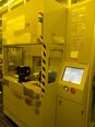
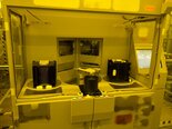
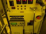
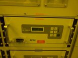
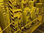
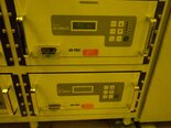
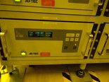
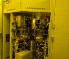
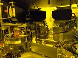
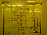
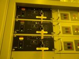
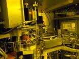
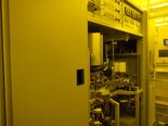
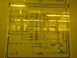
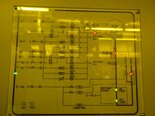

Tap to zoom

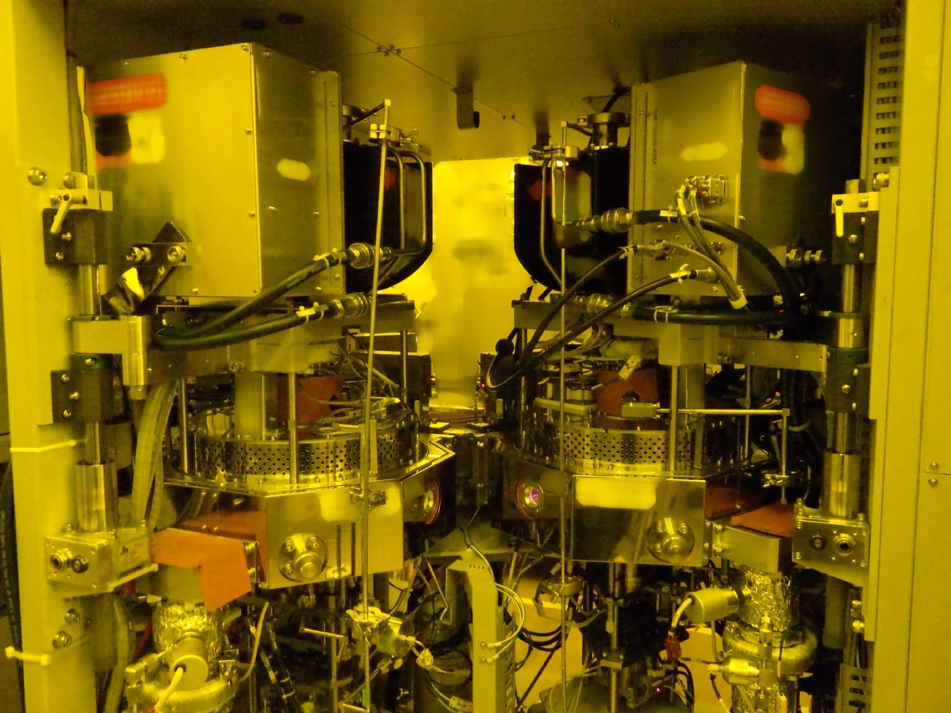
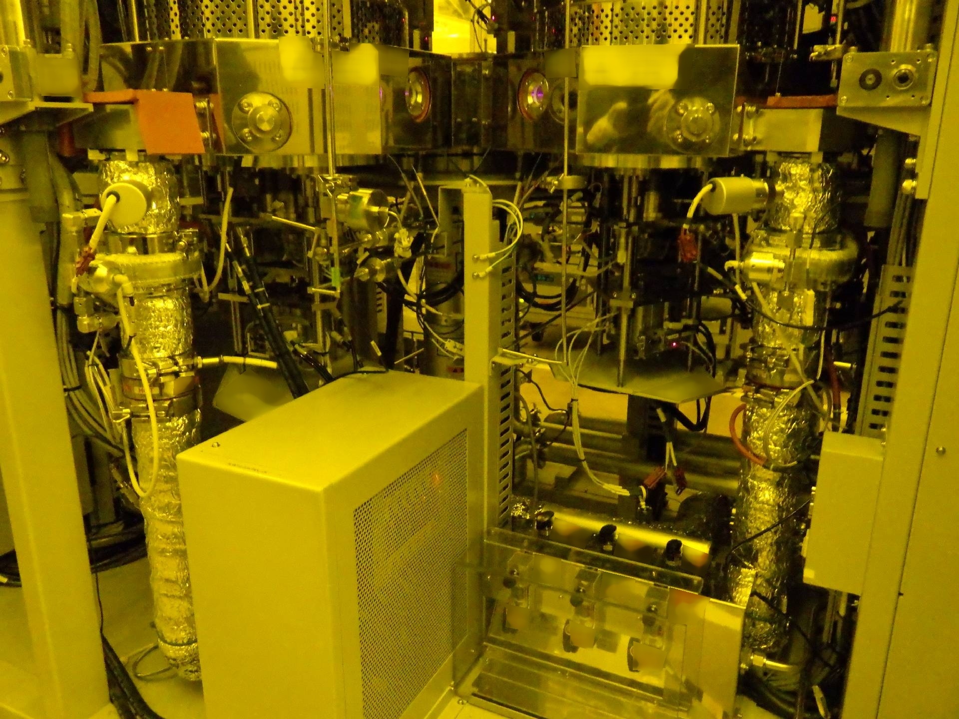
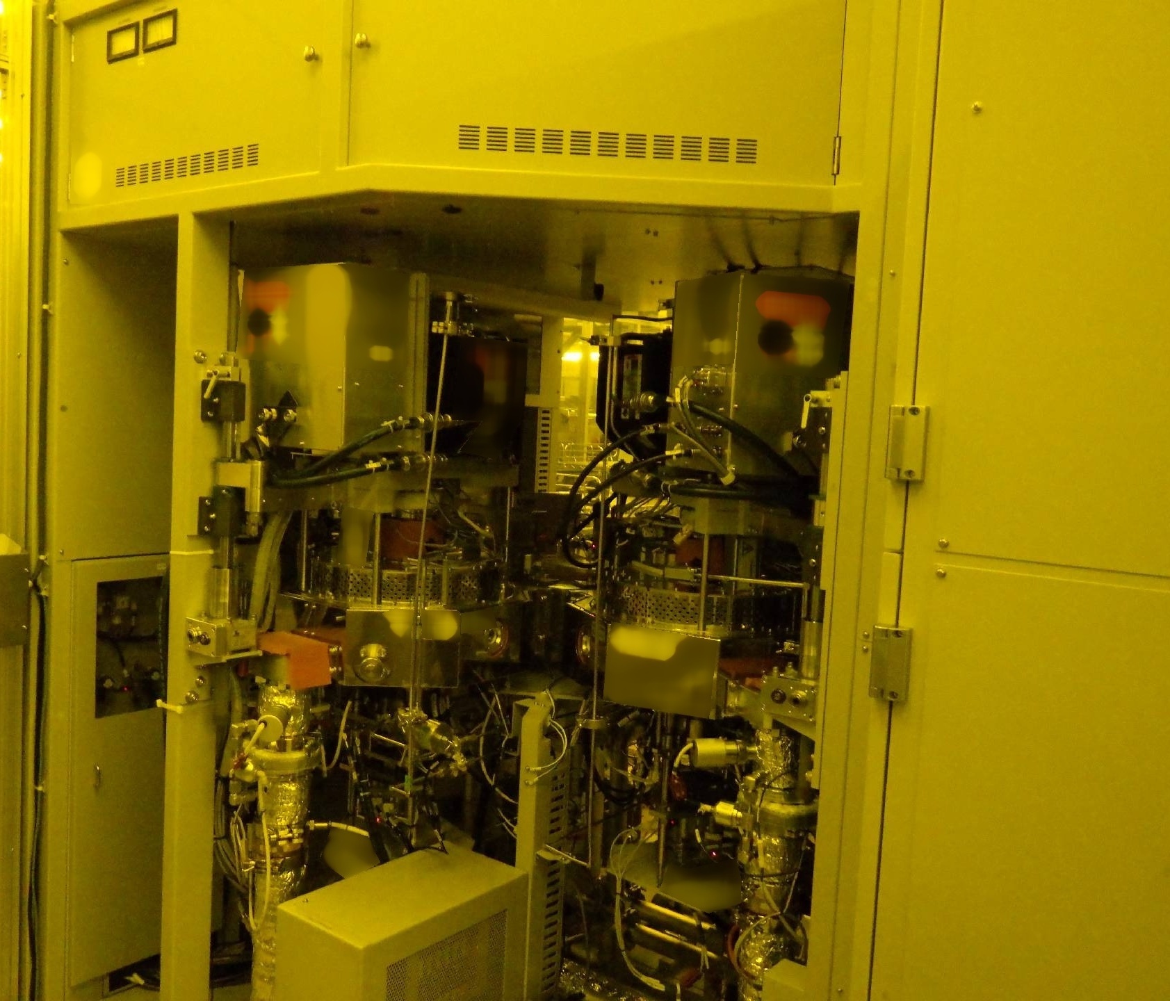
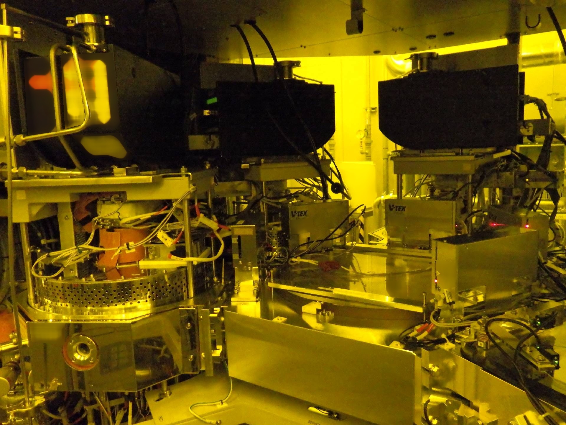
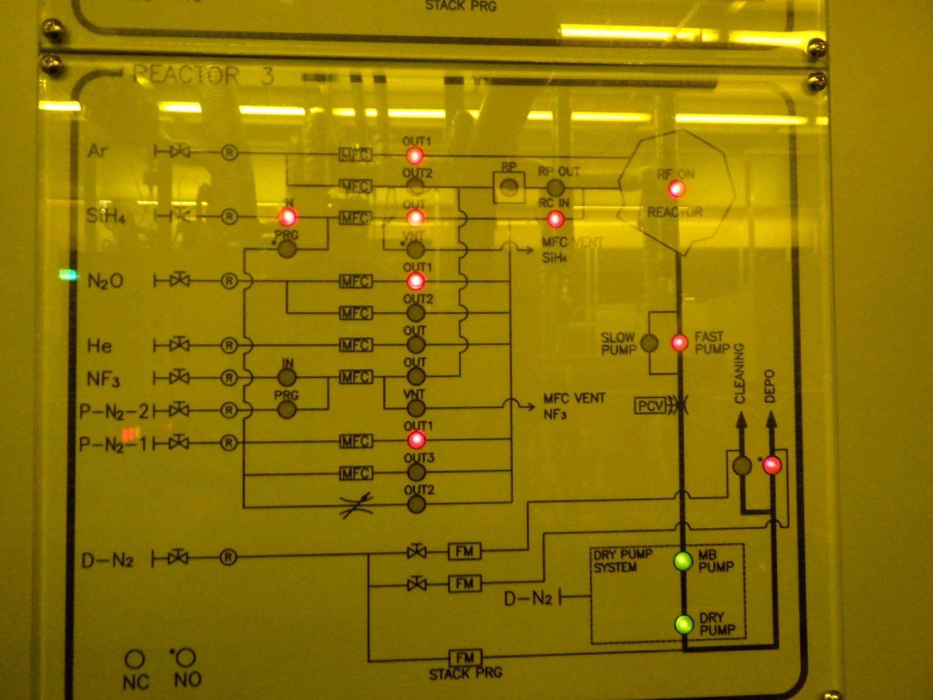
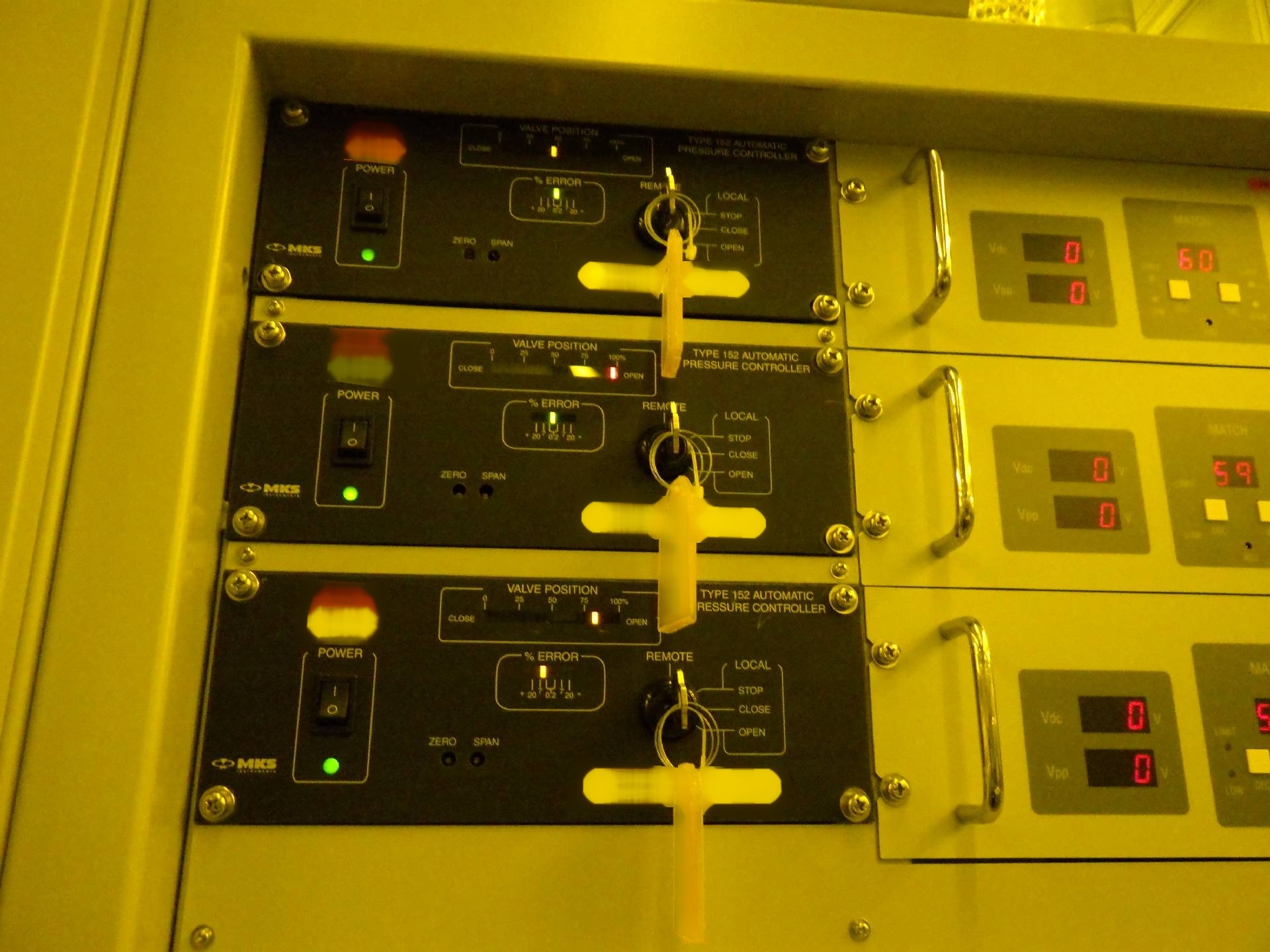
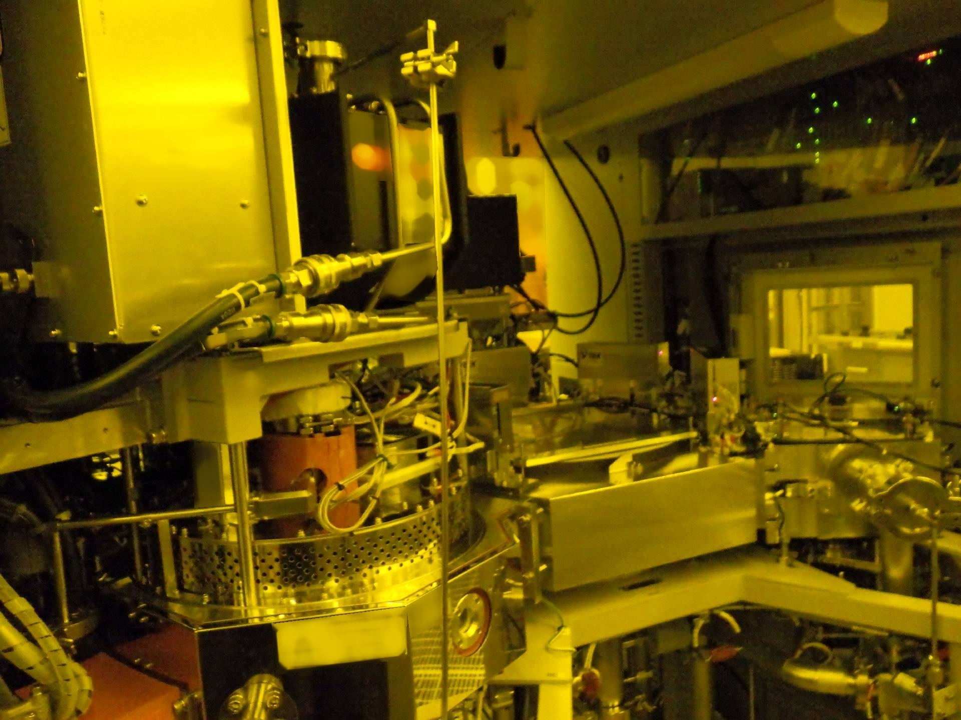
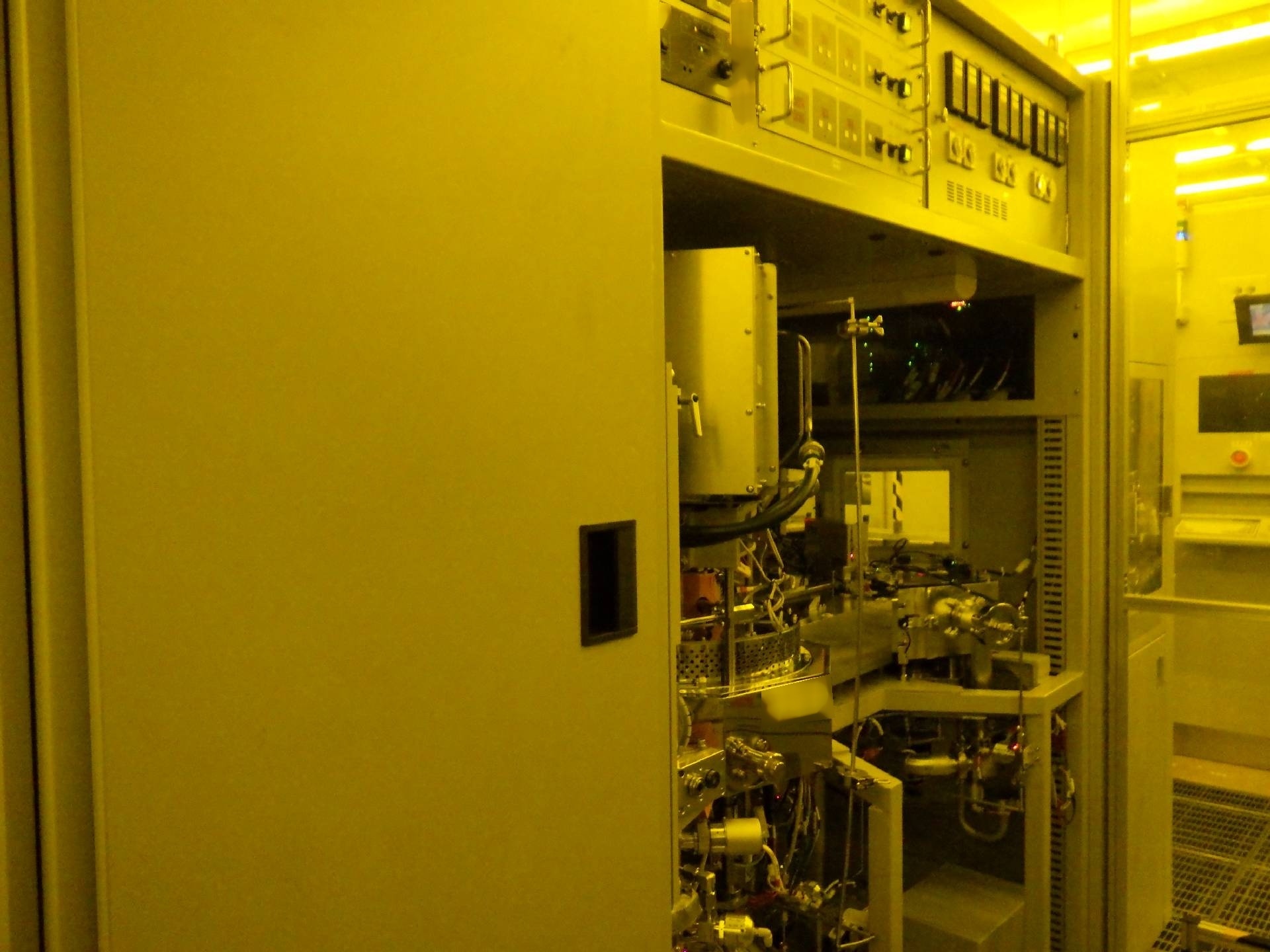
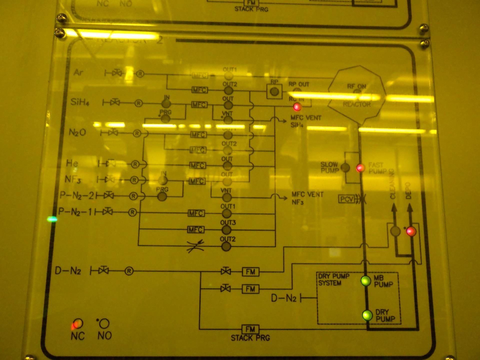
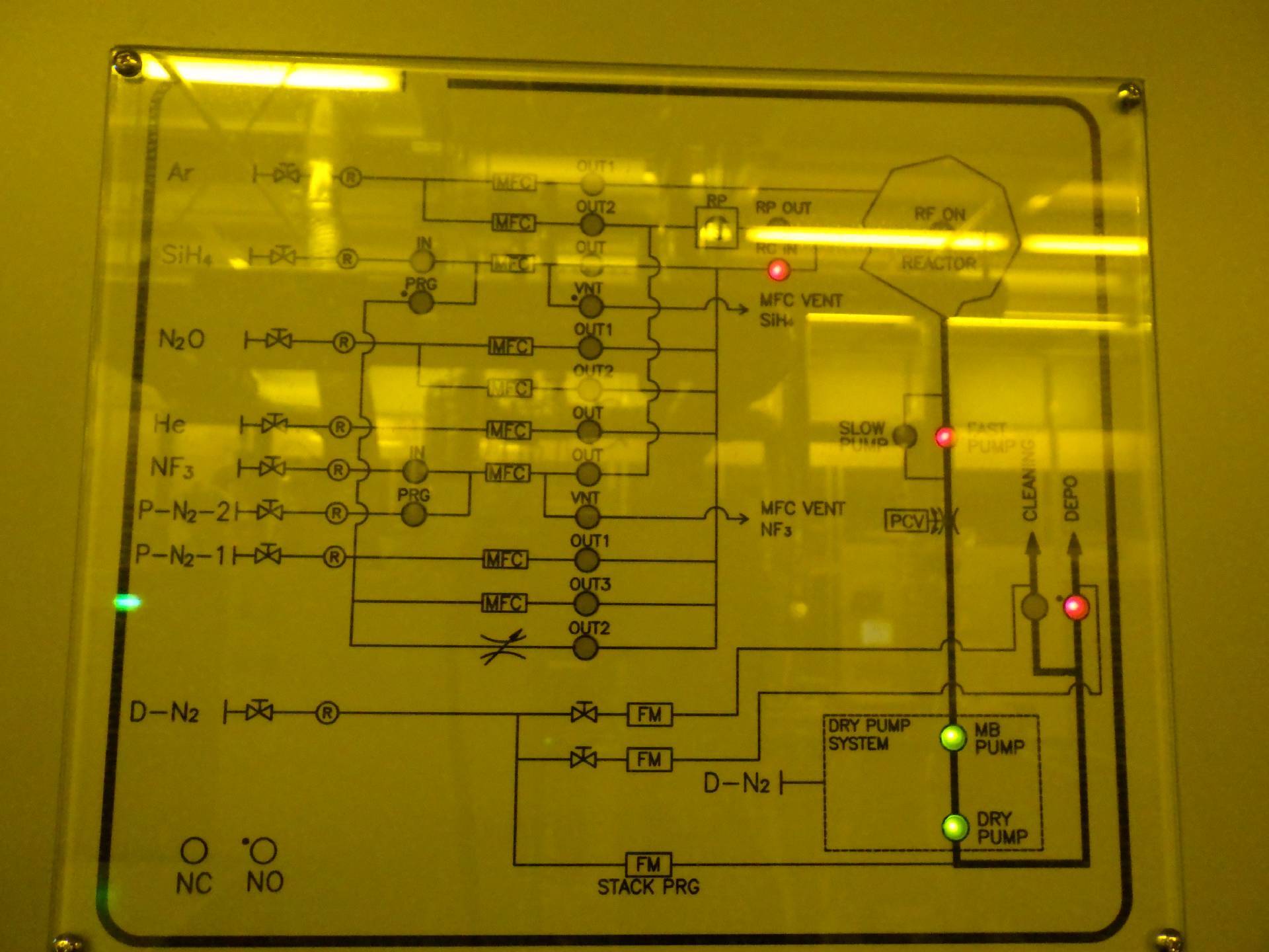
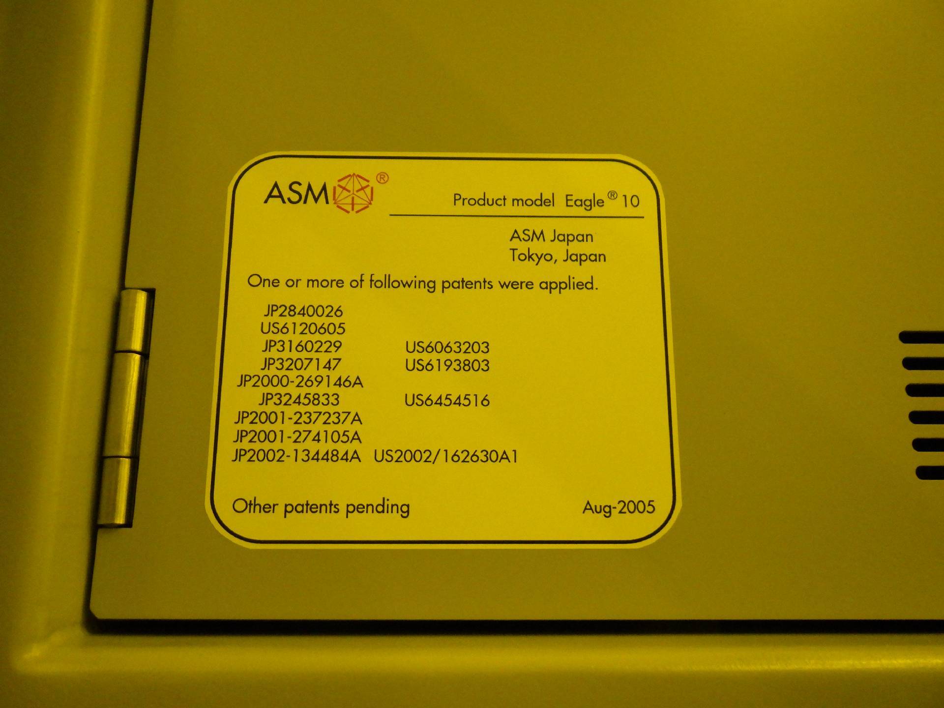
ID: 293819952
Wafer Size: 8"
Vintage: 2005
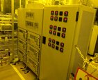
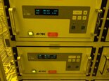
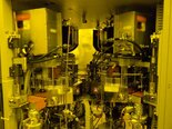
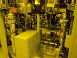
CVD System, 8"
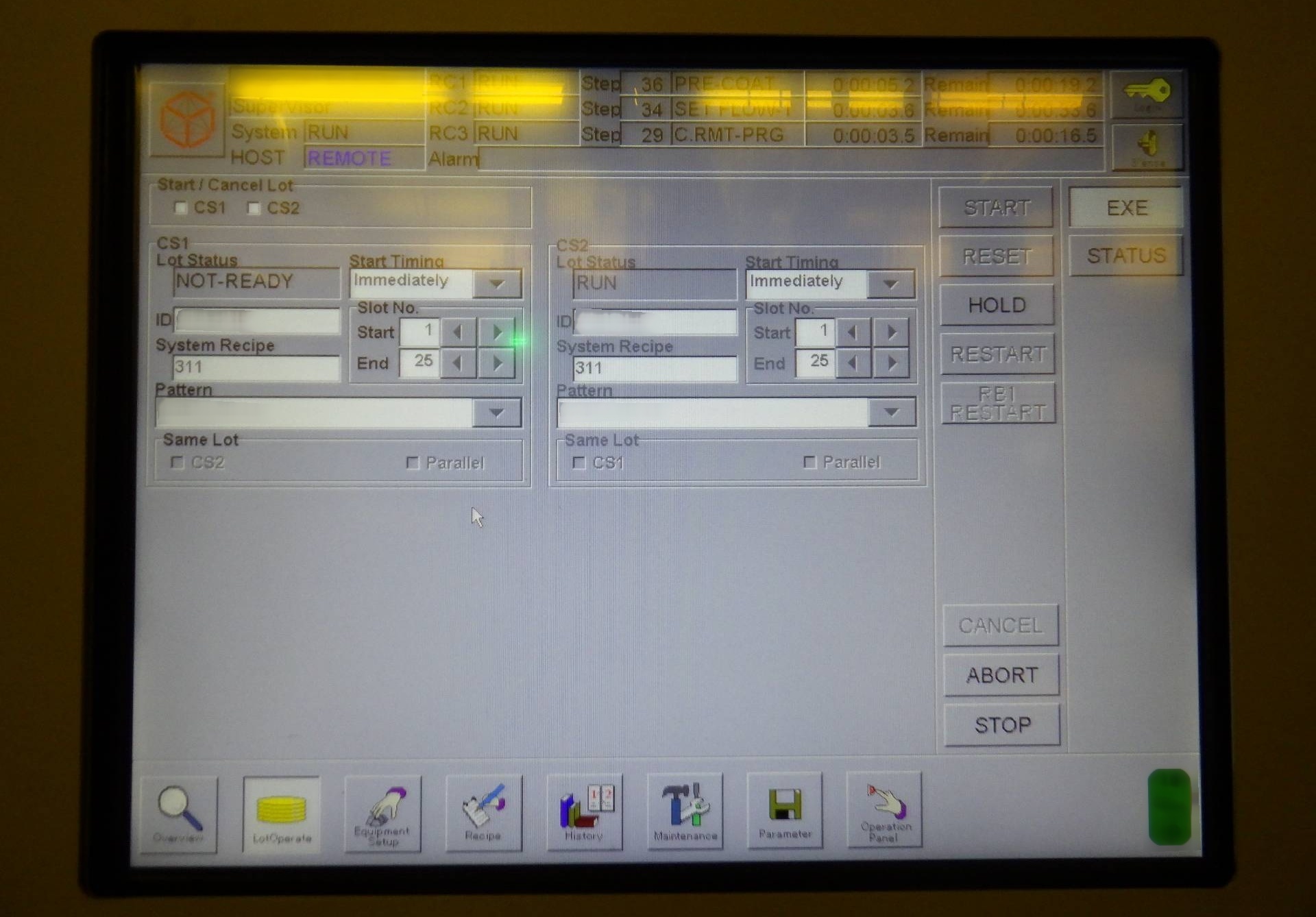
3 Channels
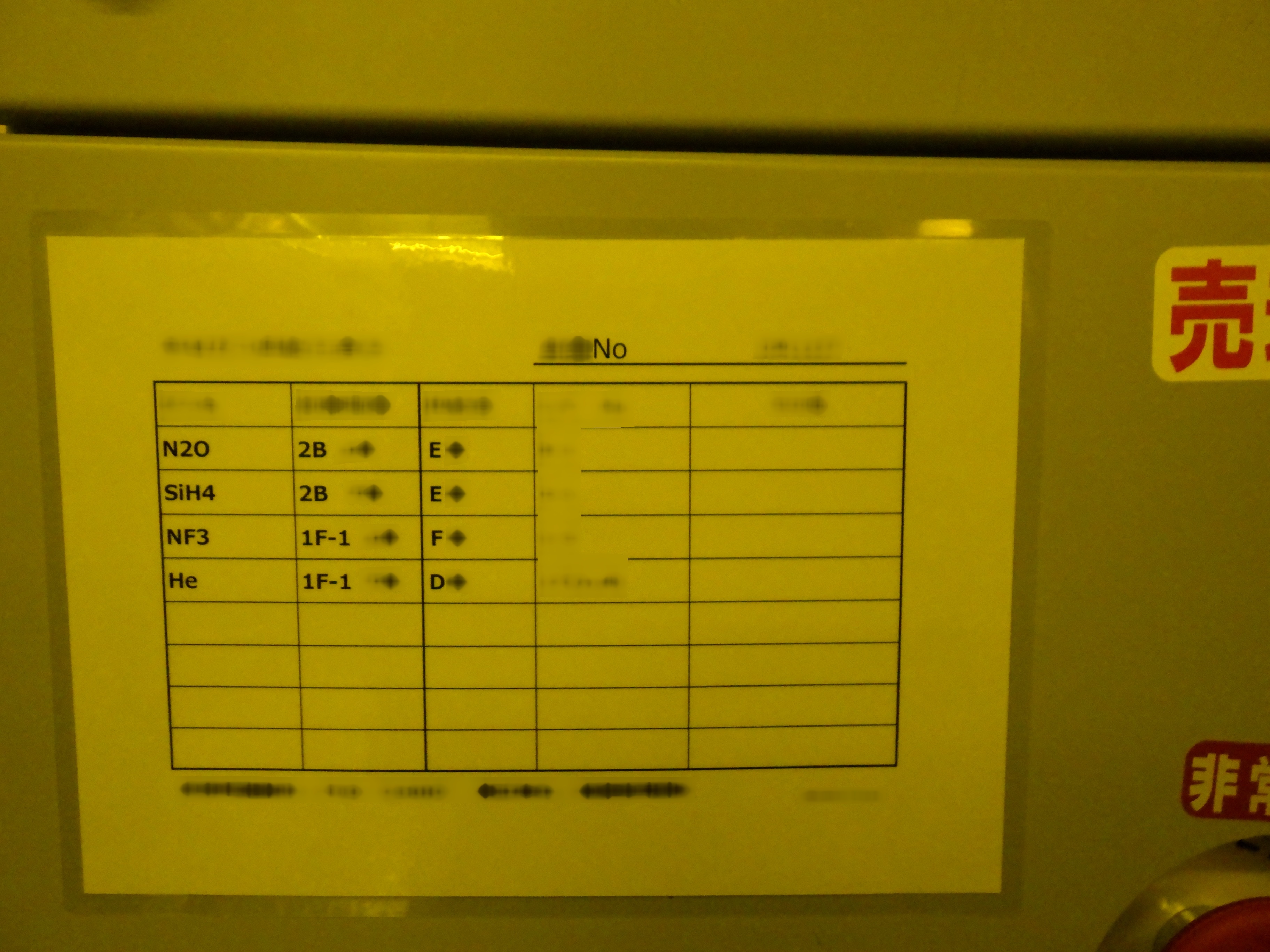
Gas: SiH4
2005 vintage.
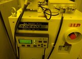
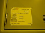
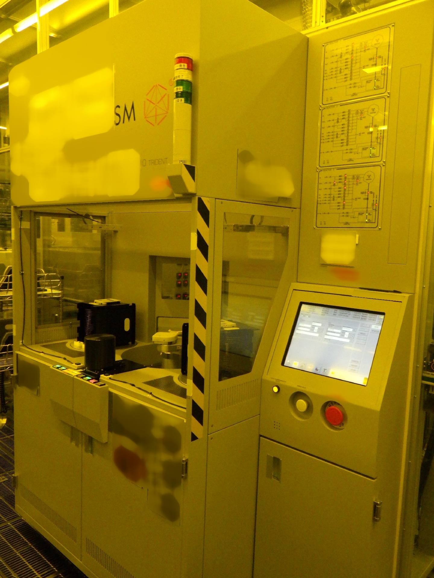
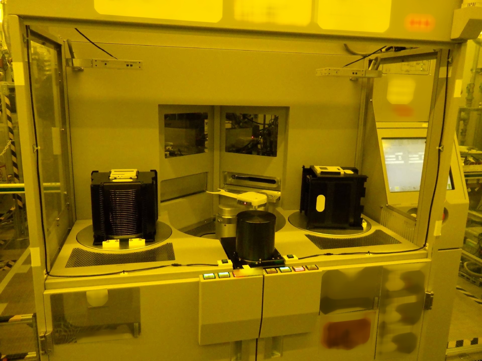
ASM Eagle 10 is a bonder designed and manufactured by ASM Pacific Technology, a leading supplier of equipment and materials to the semiconductor industry. ASM EAGLE-10 is a fully automated, self-learning bonder and was designed specifically for the production of semiconductor packages. Its features include a self-learning CCD inspection equipment, an integrated non-contact placement system, and a precise interconnection unit. Eagle 10 is well suited for high-volume semiconductor package production. Its high speed, accuracy, and reliability make it a perfect choice for bonding applications. EAGLE-10 has a maximum bond rate of 1,200 bonds per hour, with a minimum bond accuracy of 25µm. Its precise placement machine allows for precise bond alignment within a range of +/- 10µm. It is also capable of bonding packages up to 75mm. ASM Eagle 10 has an intelligent CCD inspection tool built-in that can inspect packages during the bonding process. This asset is able to detect defects, package orientation and coordinates, allowing for precise placement of packages. This technology also enables the model to recognize and repair errors, reducing mistakes and improving production efficiency. ASM EAGLE-10 also includes an advanced, non-contact placement equipment that ensures that packages are securely placed in their correct positions. This non-contact placement system is able to position packages even if they are slightly offset. This feature improves the unit's flexibility and reduces potential problems associated with off-centered packages. In addition, Eagle 10 features an integrated 3D interconnection machine. This tool is designed to bond several types of packages, including hybrids and SO-DIMMs. The asset utilizes a direct wire technology which increases the efficiency of the bonding process and reduces the overall cost of production. Overall, EAGLE-10 is the perfect choice for the production of complex semiconductor packages. Its accurate placement and inspection model, non-contact placement equipment, and 3D interconnection system make it a reliable and cost-effective solution for high-volume package production. Furthermore, its high speed and accuracy make it a perfect choice for bonding applications.
There are no reviews yet