Used LAM RESEARCH Inova #293777887 for sale
URL successfully copied!
Tap to zoom
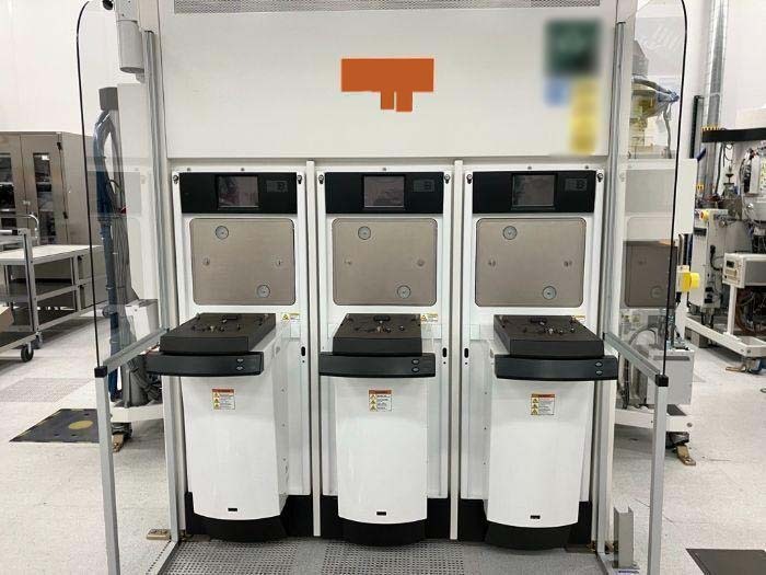

ID: 293777887
Wafer Size: 12"
Vintage: 2011
PVD System, 12"
Process: Ta, Cu
2011 vintage.
LAM RESEARCH Inova is a state-of-the-art plasma-enhanced chemical vapor deposition (PECVD) reactor system primarily utilized for thin film deposition processes in semiconductor manufacturing. As a vital tool in the fabrication of advanced semiconductor devices, Inova reactor offers precise control over film deposition parameters, enabling the creation of high-quality films with excellent uniformity and reproducibility. At the heart of LAM RESEARCH Inova reactor is its innovative design, which incorporates advanced plasma generation techniques and temperature control mechanisms to ensure optimal film growth conditions. The reactor chamber is typically made of high-purity materials such as quartz or stainless steel to minimize contamination and maintain a clean processing environment essential for semiconductor production. One key feature of Inova reactor is its capability to generate high-density plasma using radio frequency (RF) energy, which is crucial for enhancing the chemical reactions involved in thin film deposition. The plasma source, often a capacitive-coupled RF power supply, ionizes the process gases introduced into the chamber, creating a highly reactive environment conducive to film growth. The precise control of the plasma parameters, such as gas flow rates, RF power, and pressure, allows users to tailor the film properties to meet specific requirements. Temperature control is another critical aspect of LAM RESEARCH Inova reactor, as it directly influences the growth kinetics and structure of the deposited films. The reactor is equipped with a sophisticated heating system, often based on infrared lamps or resistive heating elements, to maintain a uniform temperature across the substrate surface. Additionally, the reactor chamber may be equipped with a temperature monitoring system to ensure tight control over the deposition temperature, further enhancing the film quality and reproducibility. Inova reactor supports a wide range of deposition processes, including silicon nitride, silicon oxide, and amorphous carbon films, among others. These films find applications in various semiconductor devices, such as interconnects, passivation layers, and insulating films, where properties like dielectric constant, refractive index, and stress level are crucial for device performance. In terms of scalability and throughput, LAM RESEARCH Inova reactor is designed to accommodate multiple substrates simultaneously, allowing for batch processing to increase productivity. The reactor chamber may feature wafer carriers or trays that hold several substrates, enabling efficient deposition of thin films on a larger scale while maintaining consistent film quality across all processed wafers. In conclusion, Inova reactor stands out as a versatile and reliable tool for thin film deposition in semiconductor manufacturing. Its advanced design, precise control mechanisms, and scalability make it an indispensable asset for semiconductor fabs looking to achieve leading-edge device performance and reliability through state-of-the-art thin film technology.
There are no reviews yet