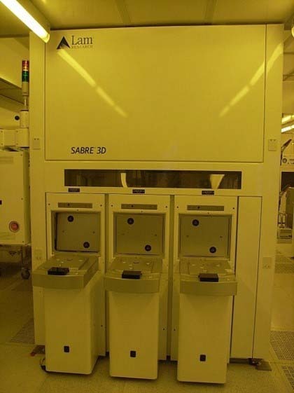
Used LAM RESEARCH Sabre 3D #9269753 for sale
It looks like this item has already been sold. Check similar products below or contact us and our experienced team will find it for you.
Tap to zoom


Sold
ID: 9269753
Plating system, 12"
Process: RDL
Operating system: Windows XP
Footprint:
Front end and back end robot
Wafer aligner
CDM for APT module
CDM for XMM module
PPT Module (2/4)
Plate A duet (1/2)
Bath module 1
Plate A flow distribution (1/2)
PMA Bath configuration: AANN
CE System settings:
Pod loader with buttons and lights-PS
Notch wafer, 12"
Standard polarity
Signal tower
EIOC Support
Advanced FA GEM and data server
HSMS Host connection
SEMI E84 Automated material handling system
Wafer history
Proteus configuration
Facilities chemical interface
Single arm front end robot
Dual arm back end robot
Real time clock timestamp source
Wafer aligner
CWS Wafer size detection
Single clamshell lift controller
CE Module front end settings:
IOC Type: Ethernet based IOC
(25) Wafers per cassette
SEMI E84 Automated cassette transfer
Active wafer centering
CA Event mode
(3) Load ports
Traverser (slide axis) vacuum robot
Ethernet pod loader communication
Extended fix loader command mode
With pod present sensor
Standard fix loader hardware
With pod present sensor
Default AMHS setting
Serial Port RFID communication
PPT2 AWC Enabled checking firmware
Robot pod loader map source
Pod loader, 13"
CE Module CDM for APT module:
ADM Process delivery: DI Process
CE Module CDM for XMM module:
PCDM Module type: SRD Configuration module
CE Module PPT module 2:
Notch wafer, 13"
Post treatment PPT module
PPT Tank type: ADM Process DI
Super cell configuration: SRD
Valve position sensors
DI Flow meter
CE Module PPT module 4:
Notch wafer, 13"
Post treatment PPT module type
Super cell configuration: SRD
Active Wafer Detection (AWD)
Valve position sensors
DI flow meters
N2 Dry
CE Module plate A duet 1 and 2:
Notch wafer, 13"
Cup and contact rinse
Separate Anode Chamber (SAC): Cascade
Serial plating power supply control
Single power supply
Cell flow meters: 5 to 50 Liters
88 I/O EIOC
Valve position sensors
SAC Flow meter
Standard SAC pump
CE Module bath module 1:
Chemical Monitoring System (CMS)
Enhanced CMS command set
Copper chemical package
Multi species dosing algorithm
(5) Species
Separate Anode Chamber (SAC): Cascade
Chemistry tray container bottles
(3) Organic dosing containers
NESLAB Heater chiller
VMS Facility request channel 1
Pump organic dose delivery
Dose pump flow switch
88 I/O EIOC
Central recirculation pump
Renner recirculation pump
Bath module 1
CE Module plate-A flow distribution 1 and 2:
FDM Flow meter: 0 to 80 LPM
Independent FDM pump
Central recirculation pump
No PMB Bath
2017 vintage.
LAM RESEARCH Sabre 3D is a high speed, direct write electron beam lithography equipment that is capable of producing three dimensional structures with feature sizes as small as 30 nanometers. It uses a unique, patent-pending field-free electron beam source that gives it unparalleled performance in speed, resolution and pattern fidelity. Sabre 3D system consists of a vacuum chamber, a motorized stage and wafer holder, an electron beam source, an imaging unit, and a control computer. The vacuum chamber creates an atmosphere of high vacuum (~10-9 torr) which is necessary for the electron beam to travel unimpeded to the wafer. The motorized stage positions the sample wafer in the chamber, and the wafer holder holds the wafer in place. The electron beam is generated and accelerated in a field-free electron column, which minimizes field scattering and deflection. The beam travels through an electro-optical imaging machine, which images the pattern onto the wafer. The tool also includes a control computer that provides the necessary signal processing and control of the imaging asset and wafer stages, and is linked to a device-specific pattern generator. This allows the user to define the desired patterns and to input them into the model. The user can easily operate and calibrate the equipment with the intuitive graphical user interface on the control computer. LAM RESEARCH Sabre 3D system is capable of imaging very high resolution patterns on wafers made of any material, including semiconductor-grade materials. It also features focused electron beam energies up to 15 keV and beam current up to 100nA, with pattern writing speeds of up to 175 wafers/hour. This allows for the creation of three dimensional structures with feature sizes as small as 30 nm. Sabre 3D unit is an invaluable tool for research and development of new materials and fabrication processes, particularly those involving nano-scale structures. This machine provides a cost-effective, high performance solution to the challenges posed by atomically precise manufacturing. It is the ideal choice for researchers and manufacturers who require ultimate precision and speed.
There are no reviews yet