Used TEL / TOKYO ELECTRON TM #293809017 for sale
URL successfully copied!
Tap to zoom
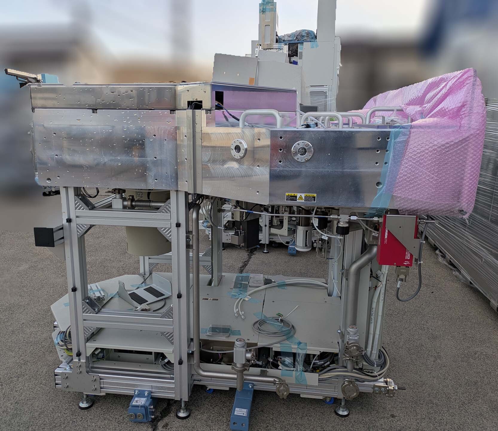

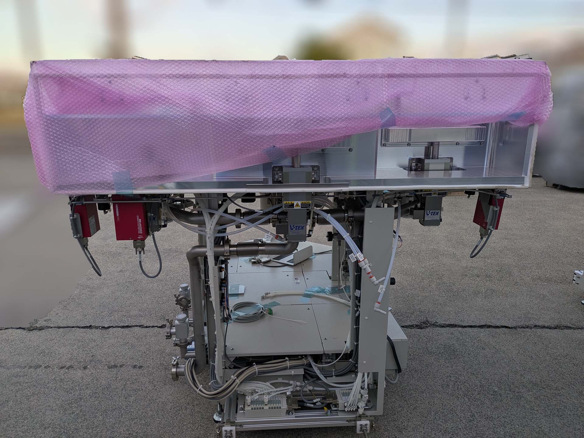
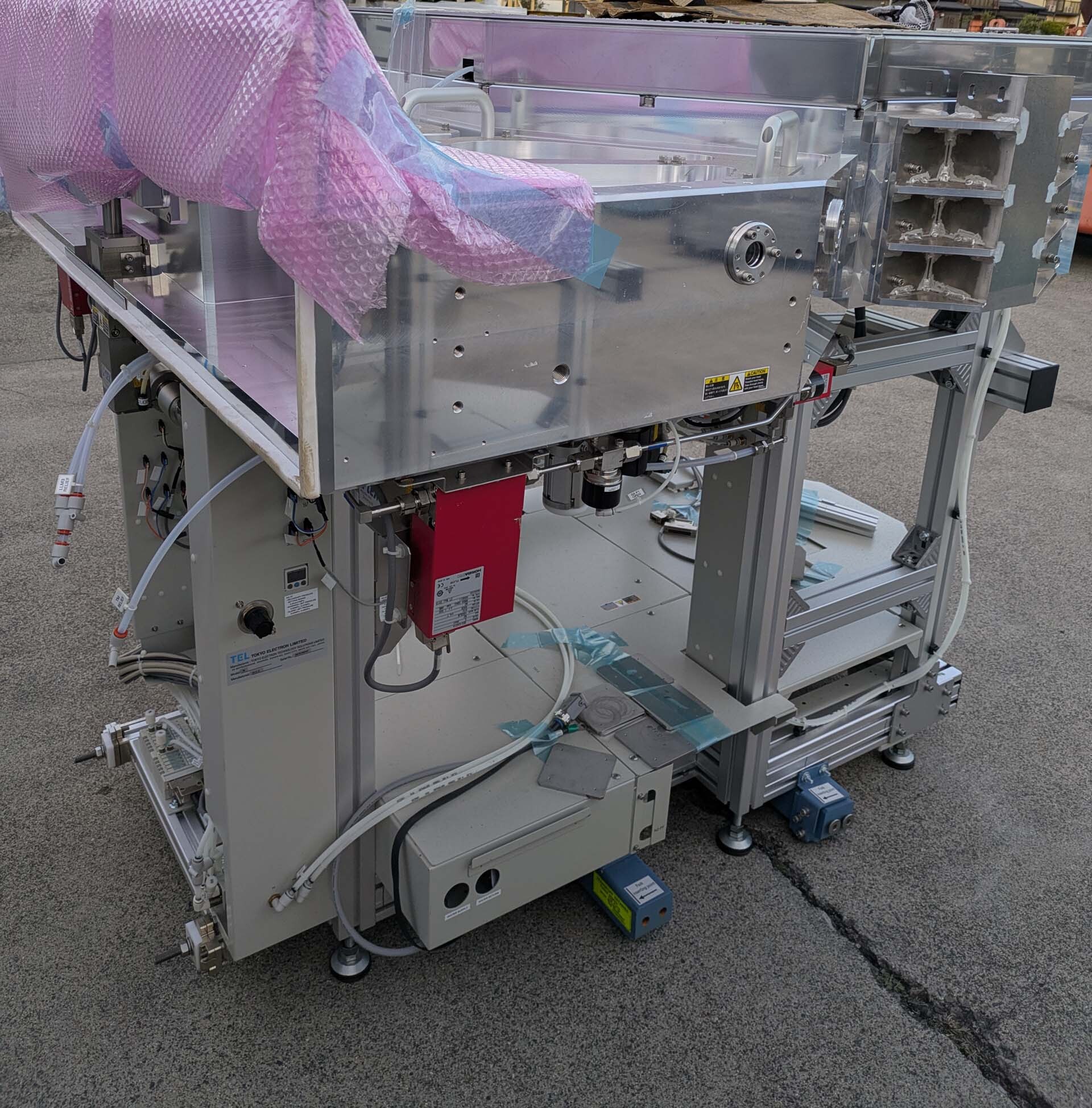
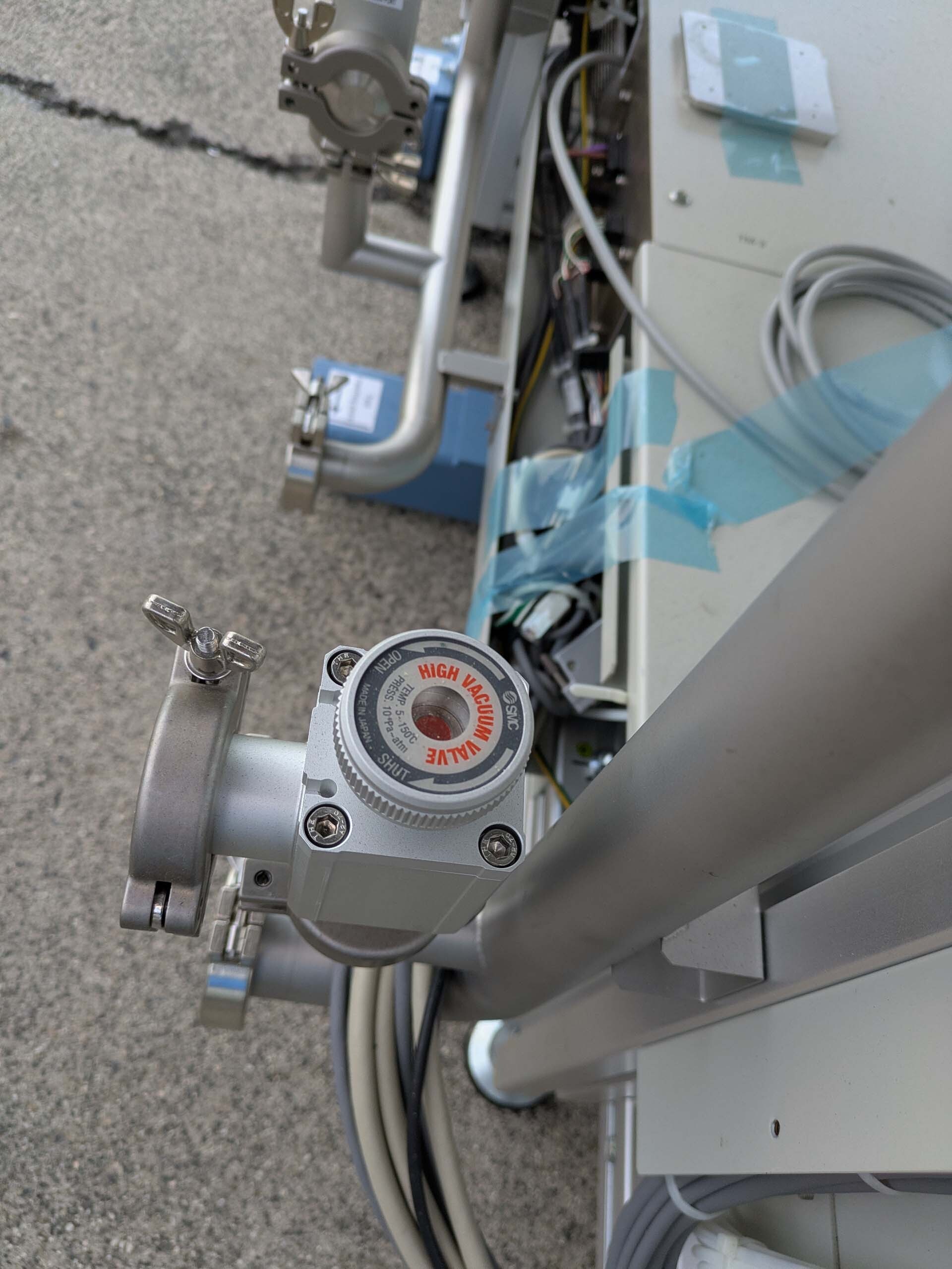
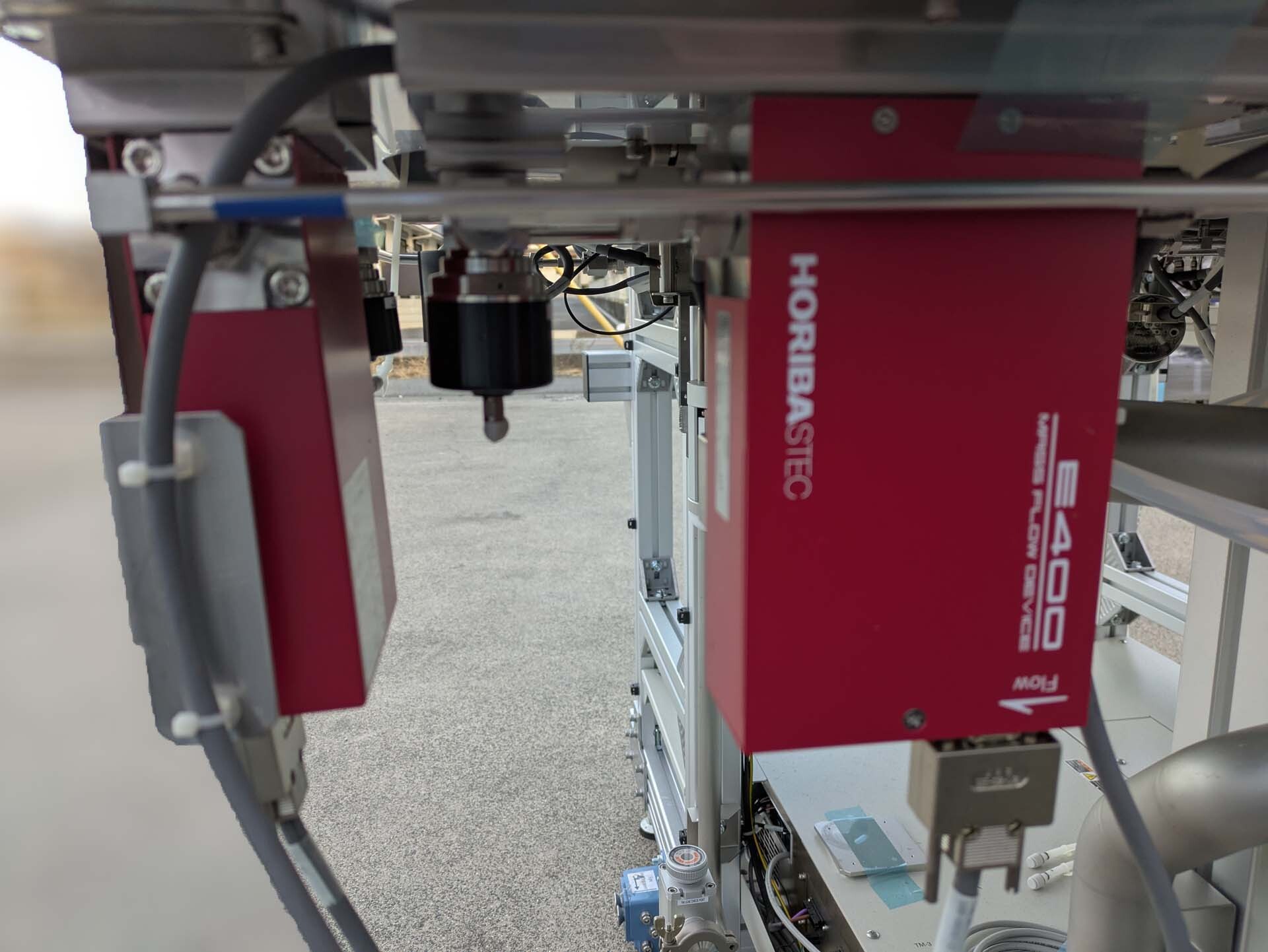
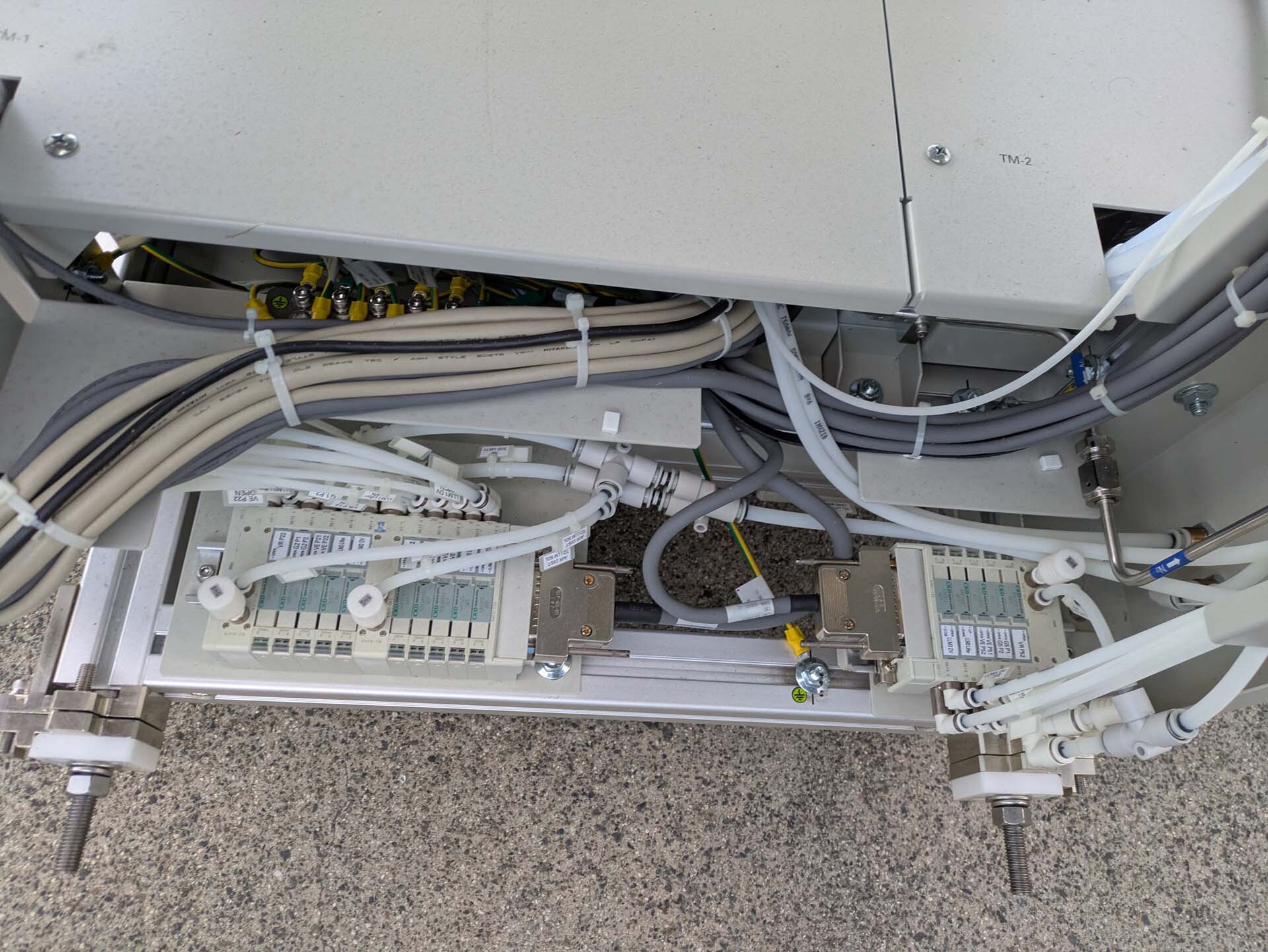
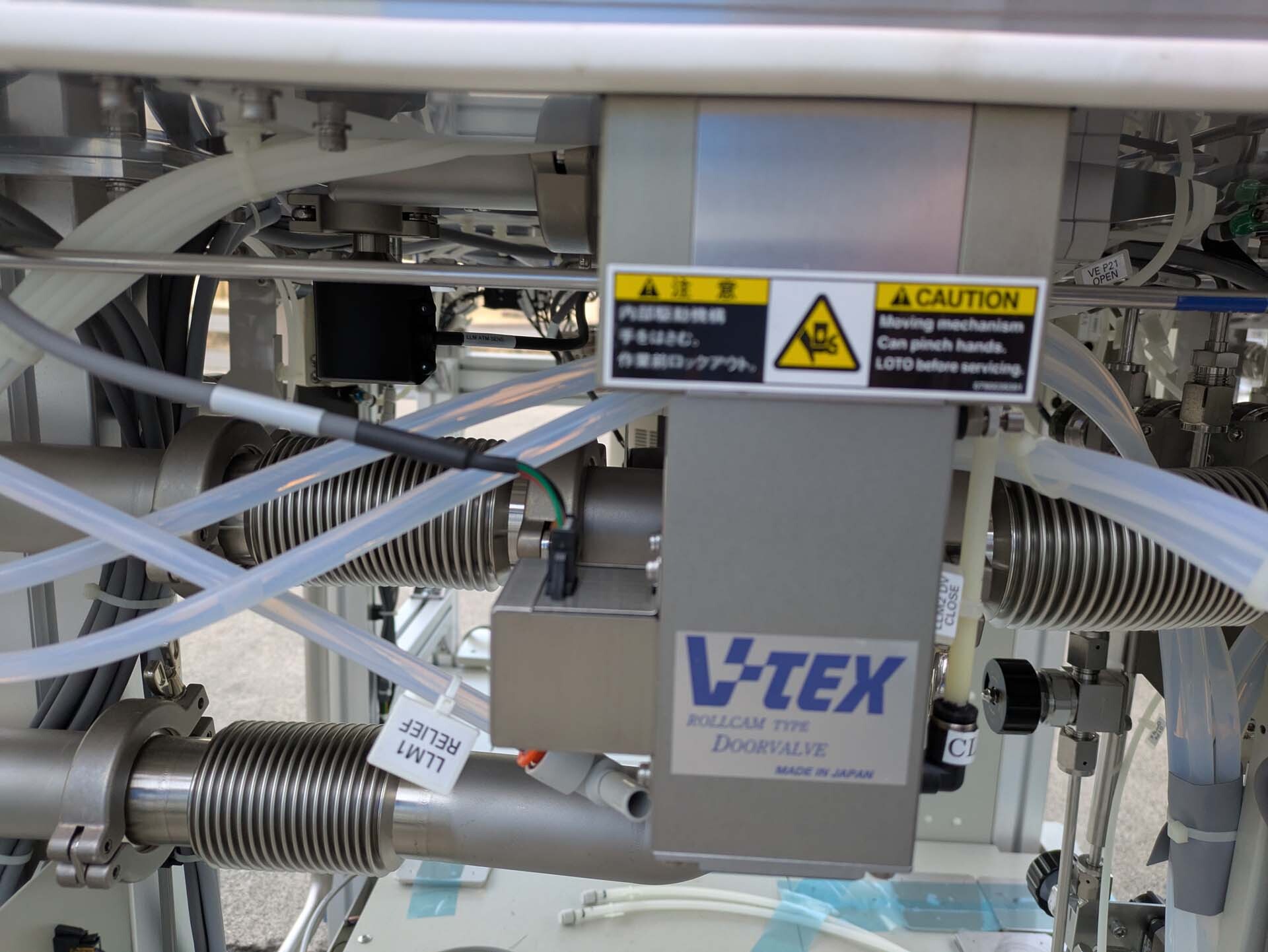
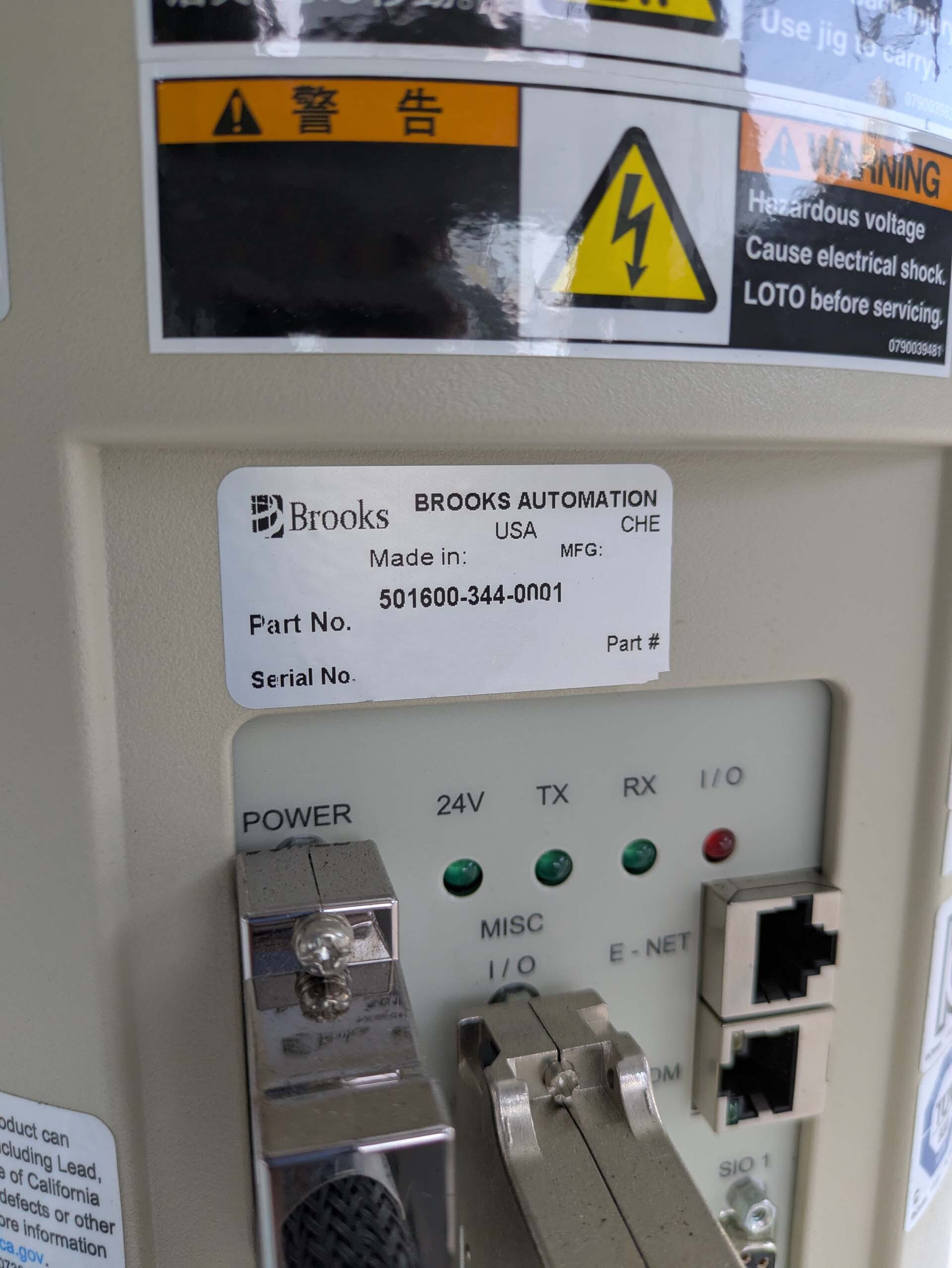
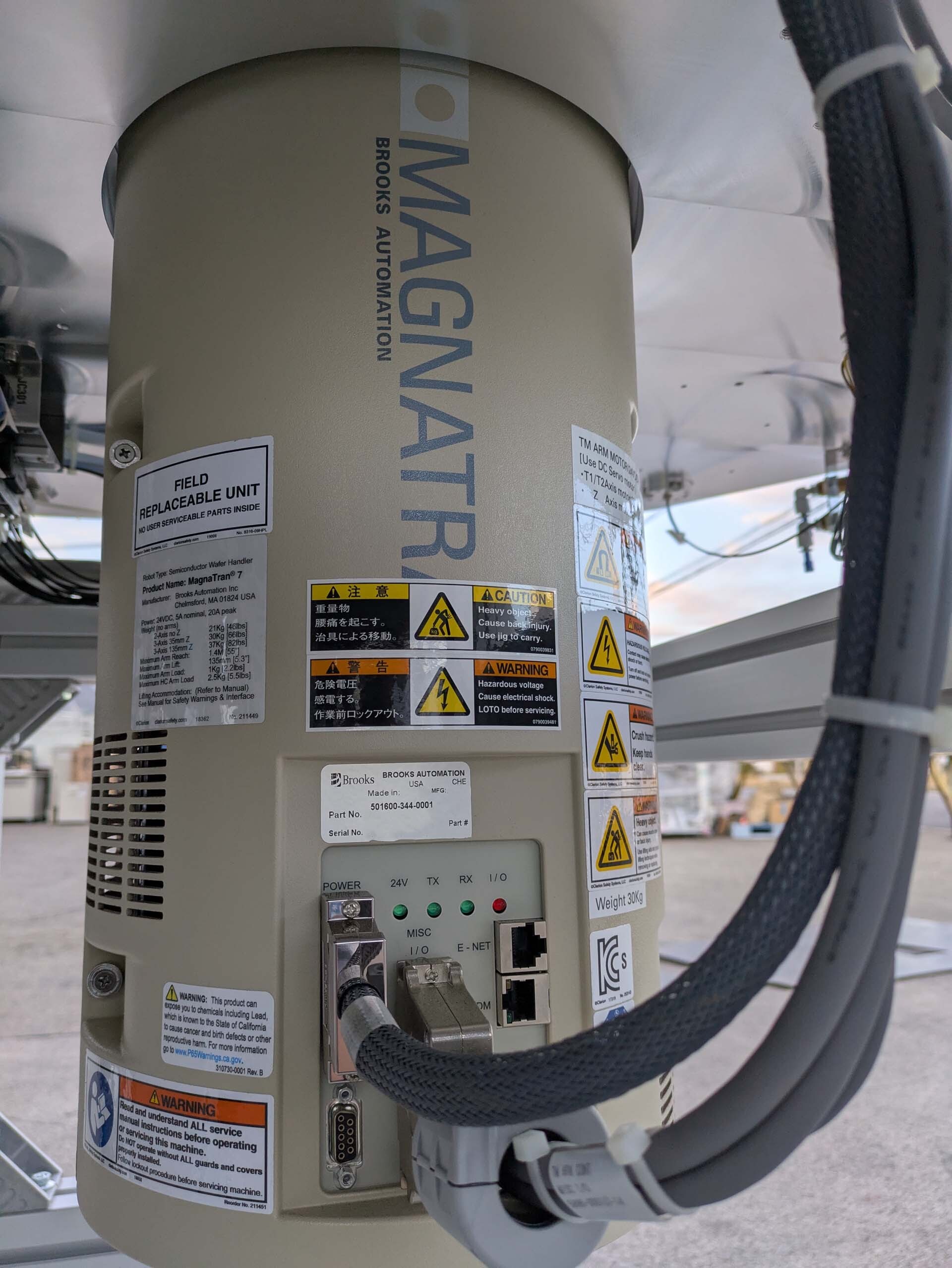
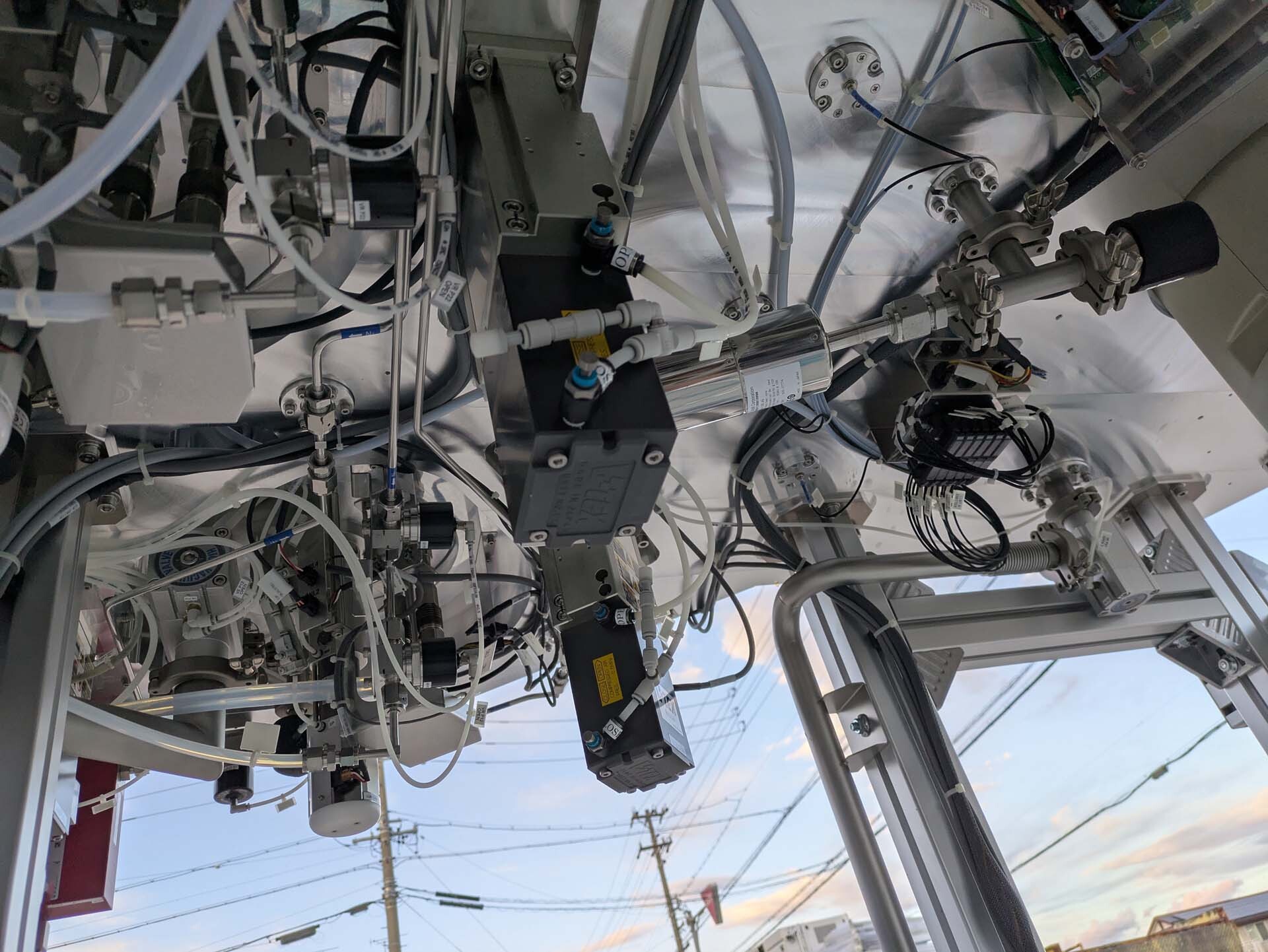
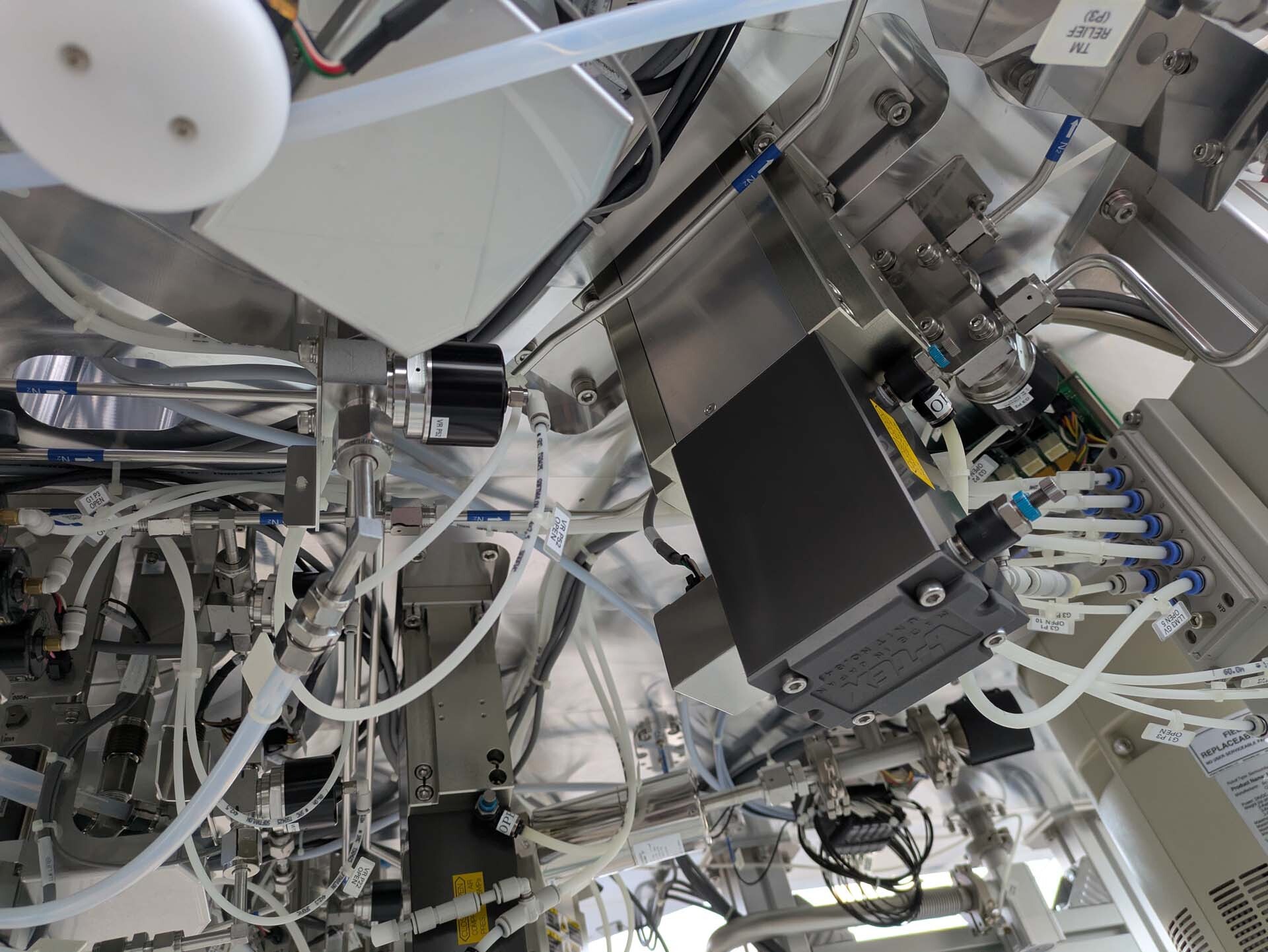
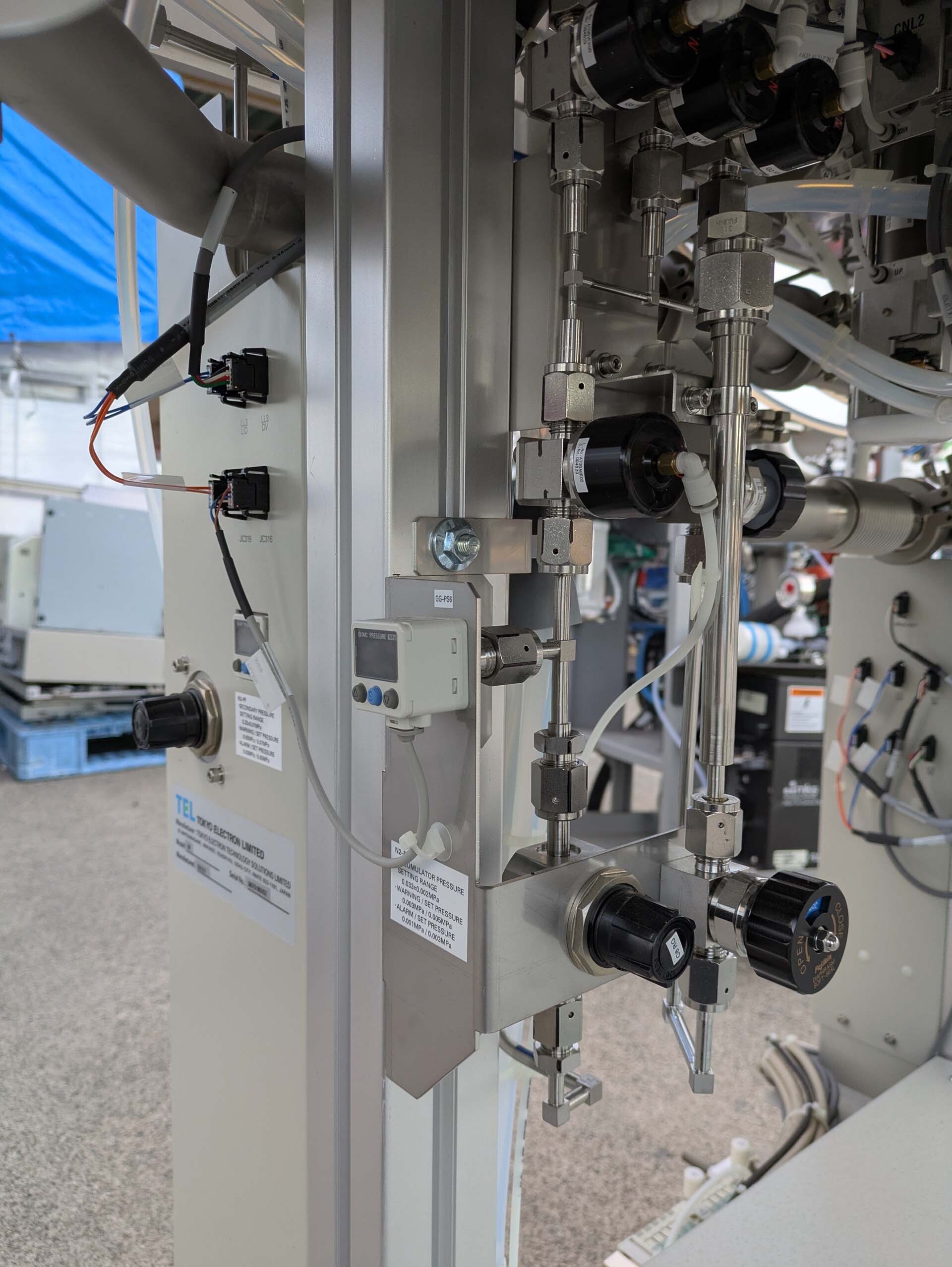
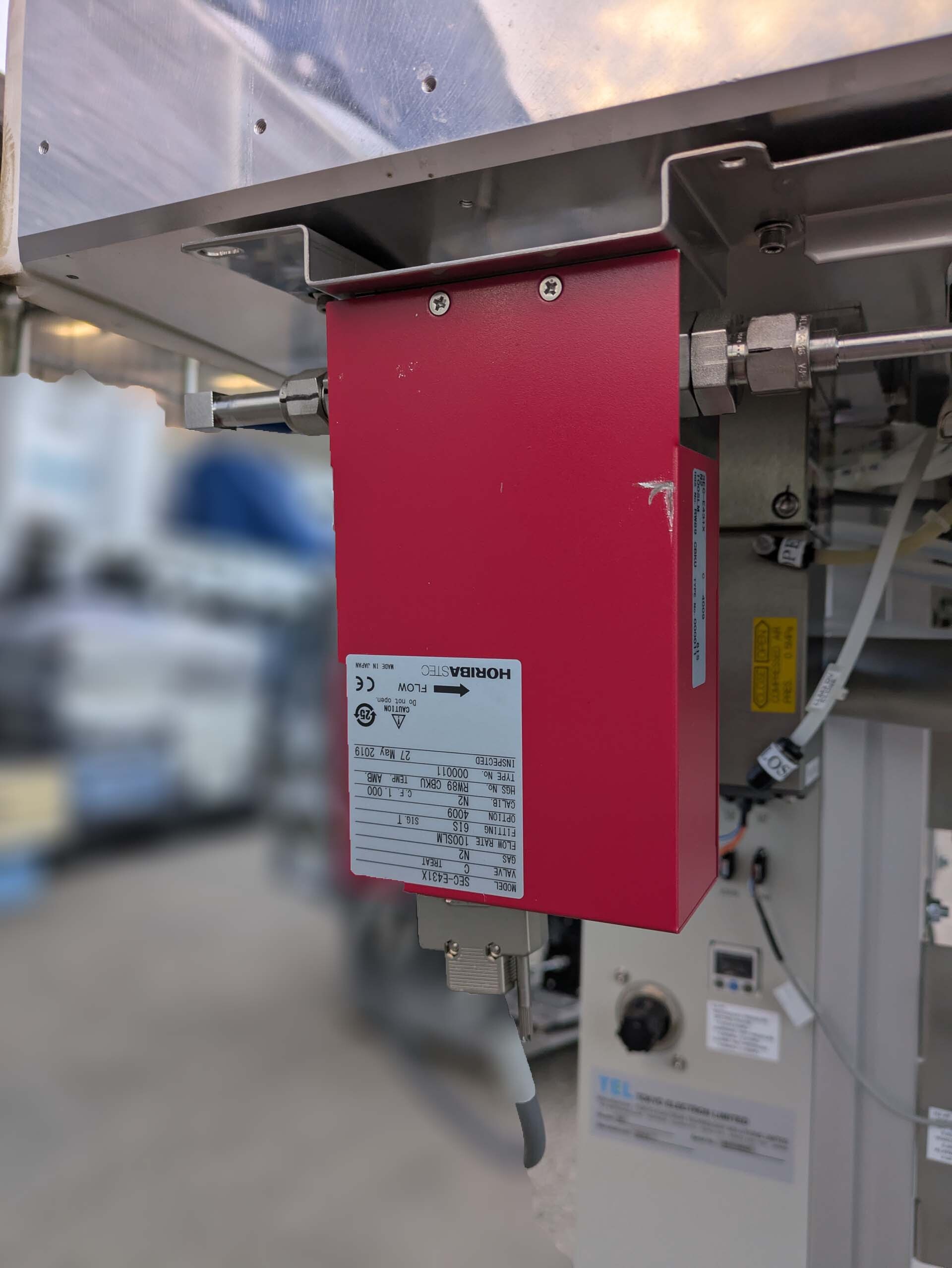
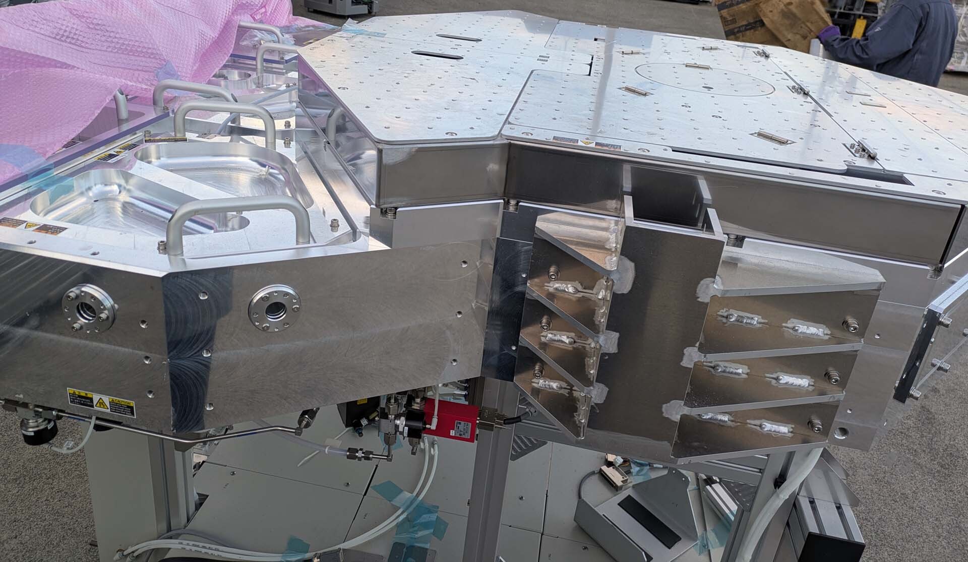
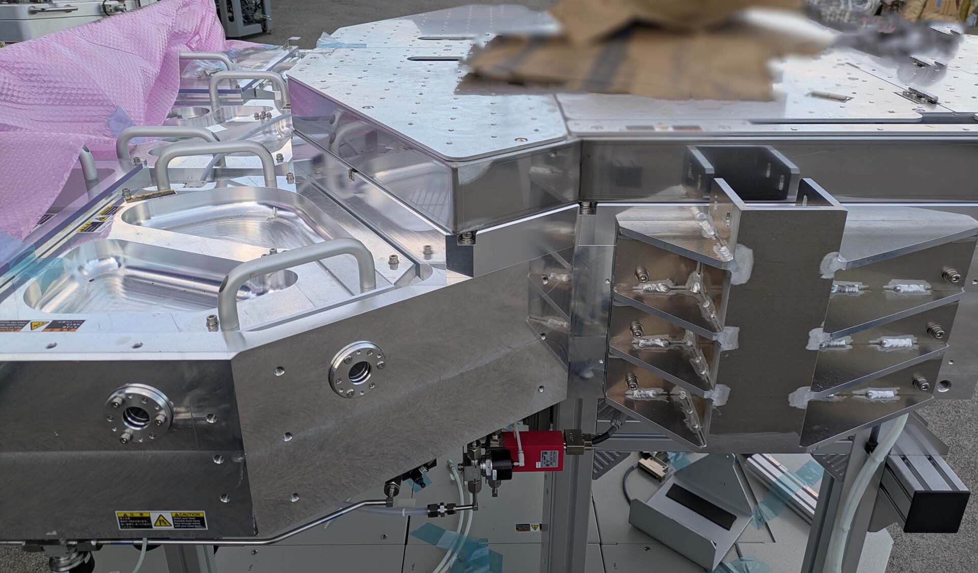
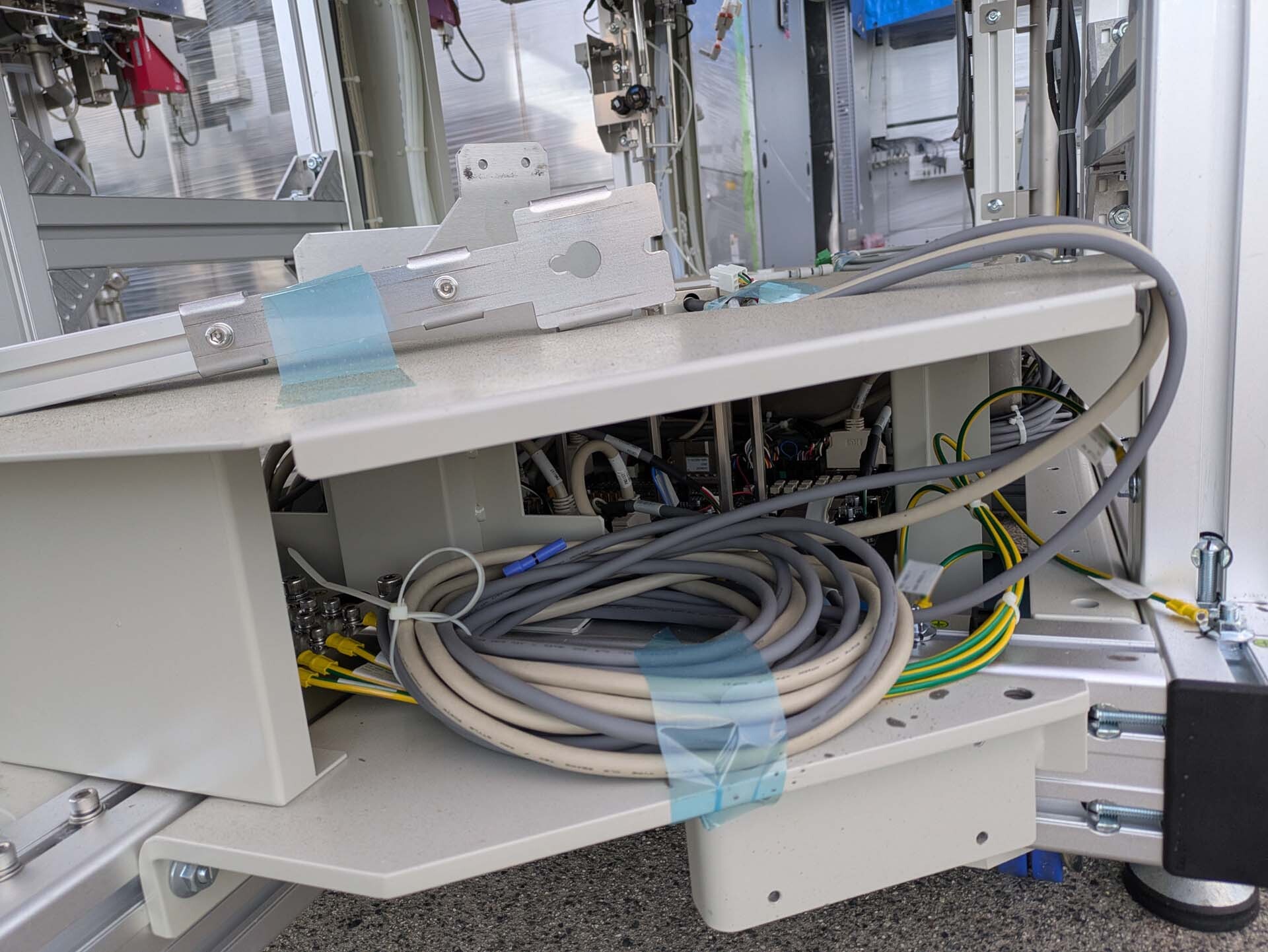
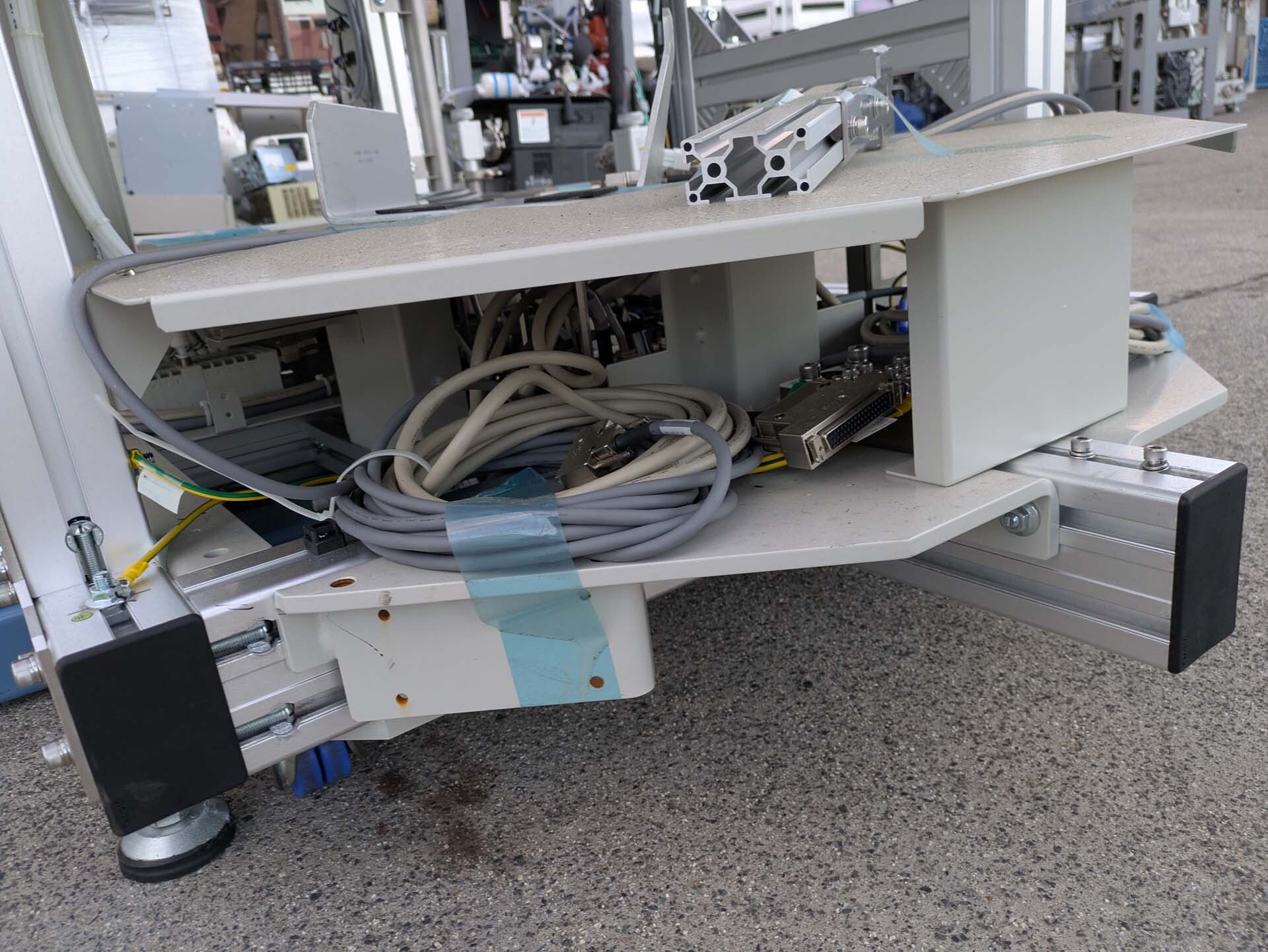
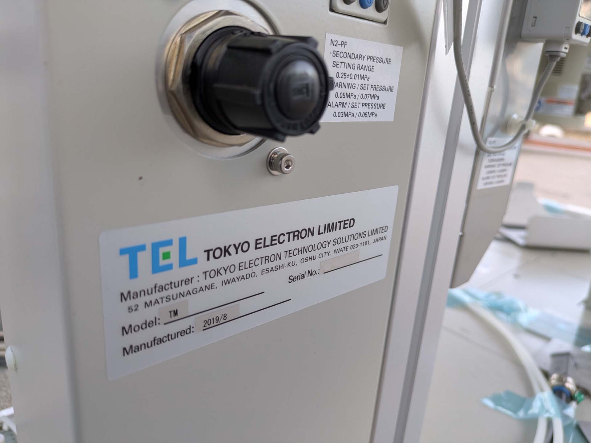
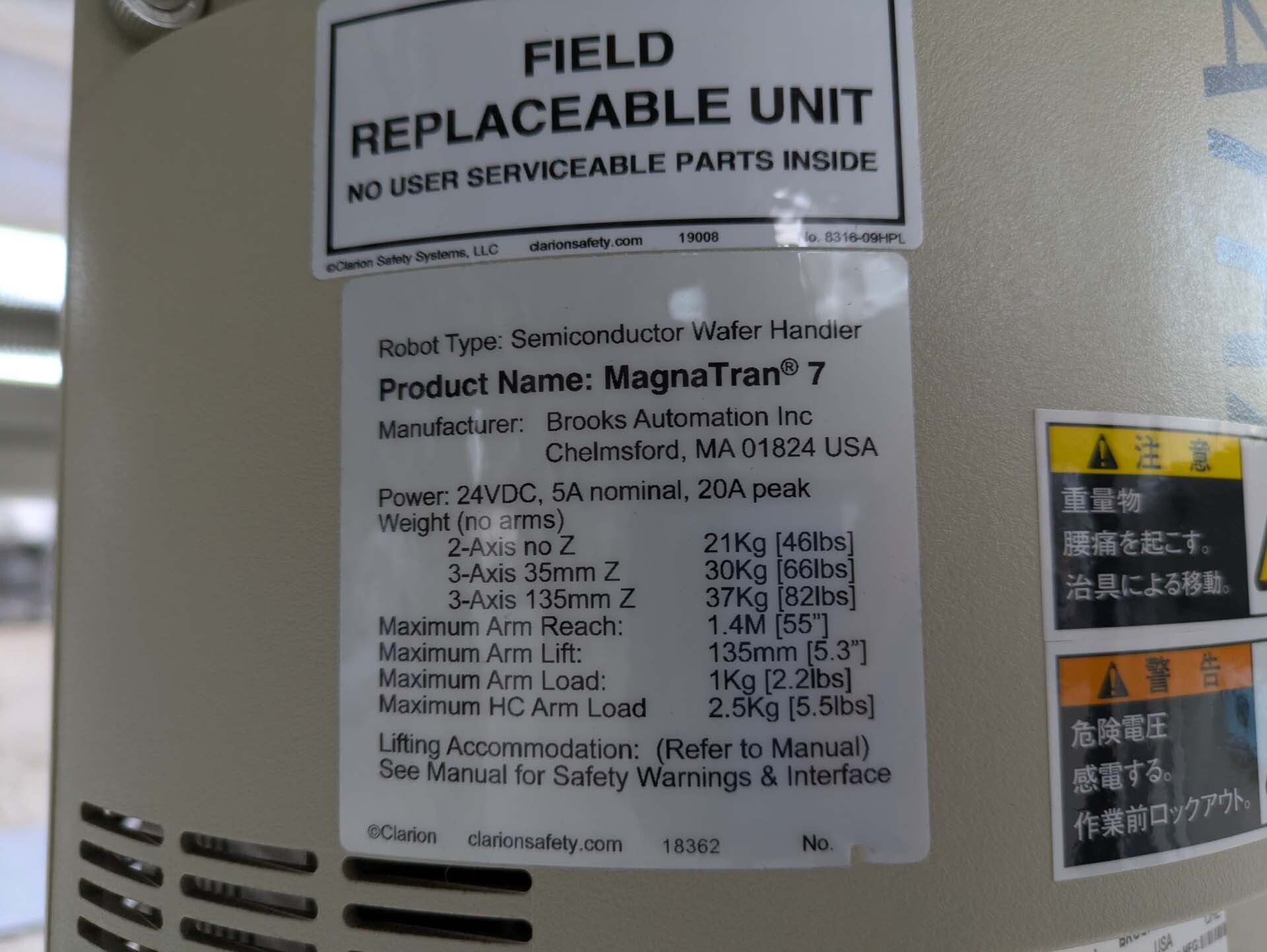
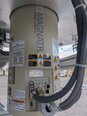
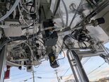
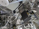
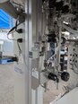
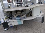
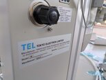
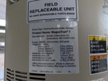
TEL / TOKYO ELECTRON TM, also known as TEL, is a leading global supplier of semiconductor and flat panel display production equipment. Founded in 1963 in Tokyo, Japan, TOKYO ELECTRON has established itself as a key player in the semiconductor industry, providing innovative solutions for advanced manufacturing processes. One of TEL / TOKYO ELECTRON flagship products is TEL reactive ion etch (RIE) reactor, a critical tool in the fabrication of semiconductor devices. The RIE process involves using reactive gases to selectively remove material from a substrate, allowing for precise pattern transfer and etching of features on the wafer surface. TOKYO ELECTRON RIE reactor is designed to deliver high etch rates, exceptional uniformity, and superior process control to meet the stringent requirements of advanced semiconductor manufacturing. TEL / TOKYO ELECTRON RIE reactor features a robust chamber design with multiple gas inlets, RF power sources, and advanced plasma control technologies to achieve optimal process performance. The reactor chamber is typically made of highly durable materials such as aluminum or stainless steel to withstand the harsh chemical environments required for etching processes. The chamber is equipped with gas distribution systems to ensure uniform delivery of reactive gases to the wafer surface, allowing for precise etching control across the entire wafer. One key feature of TEL RIE reactor is its advanced plasma source technology, which plays a critical role in generating and sustaining the plasma needed for the etching process. The plasma source typically consists of an RF generator that delivers high-frequency power to create a plasma discharge in the reaction chamber. TOKYO ELECTRON plasma source technology is designed to provide stable plasma conditions, precise control of ion energy, and efficient gas dissociation, resulting in high etch rates and superior pattern transfer fidelity. In addition to plasma source technology, TEL / TOKYO ELECTRON RIE reactor is equipped with advanced endpoint detection systems to monitor the etching process in real-time. Endpoint detection helps to accurately determine when the desired etch depth has been achieved, allowing for precise control of process parameters and ensuring consistent etching results from wafer to wafer. TEL endpoint detection systems utilize optical emission spectroscopy (OES), quartz crystal microbalance (QCM), or other sensing technologies to monitor chemical reactions and physical changes occurring during the etching process. Moreover, TOKYO ELECTRON RIE reactor is designed to support a wide range of semiconductor materials, including silicon, silicon dioxide, metal films, and III-V compounds, making it a versatile tool for a variety of etching applications in semiconductor device fabrication. The reactor can be configured with different process recipes, gas chemistries, and wafer handling options to accommodate specific customer requirements and process needs. Overall, TEL / TOKYO ELECTRON RIE reactor stands out for its advanced process capabilities, robust chamber design, and superior performance in semiconductor etching applications. With a strong focus on innovation and customer collaboration, TEL continues to push the boundaries of etch technology to meet the evolving demands of the semiconductor industry and drive the development of next-generation devices and applications.
There are no reviews yet