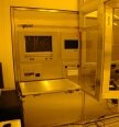
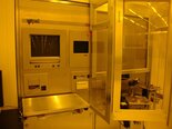
Used AMAT / APPLIED MATERIALS OPAL 7830I #9226431 for sale
URL successfully copied!
Tap to zoom






ID: 9226431
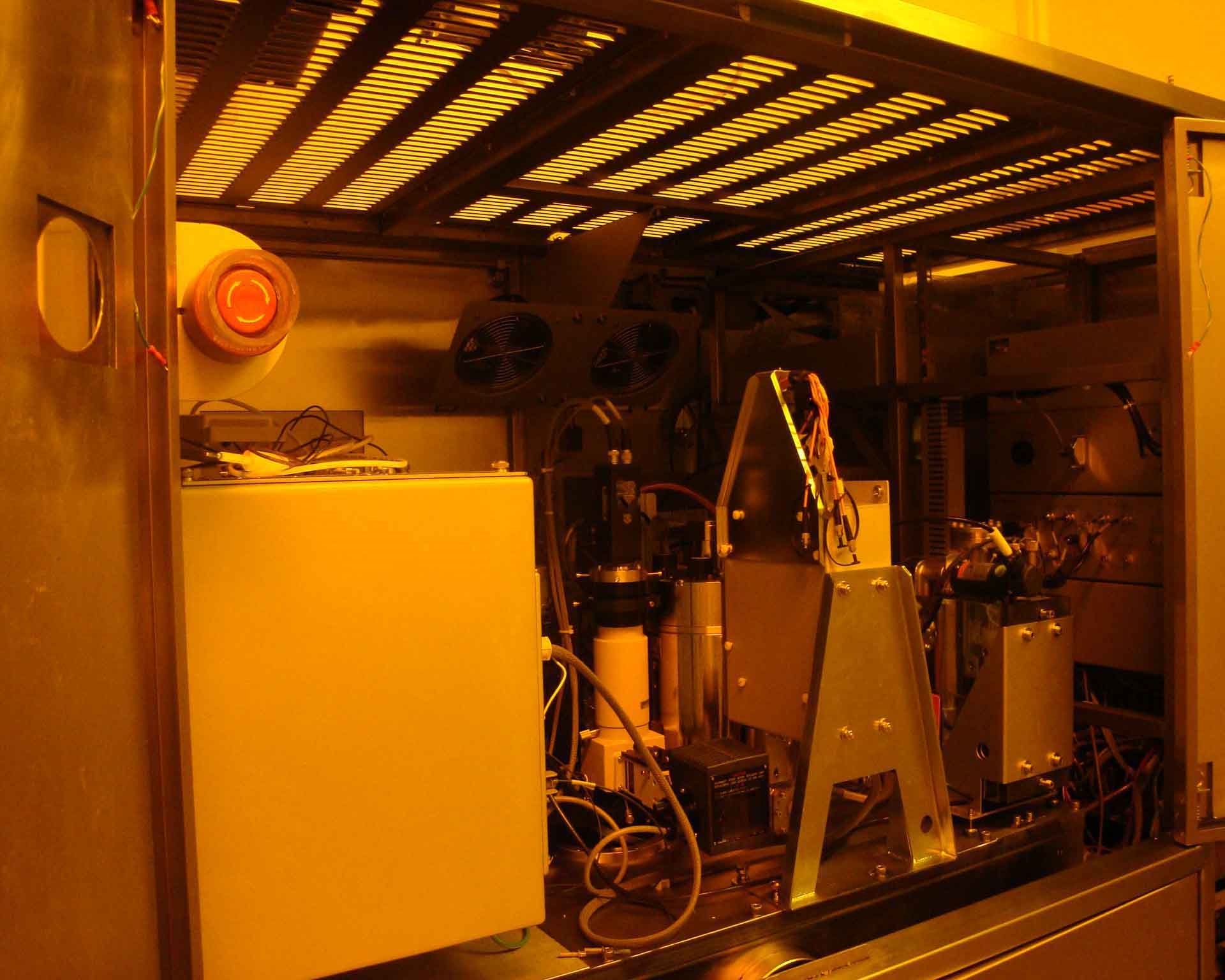
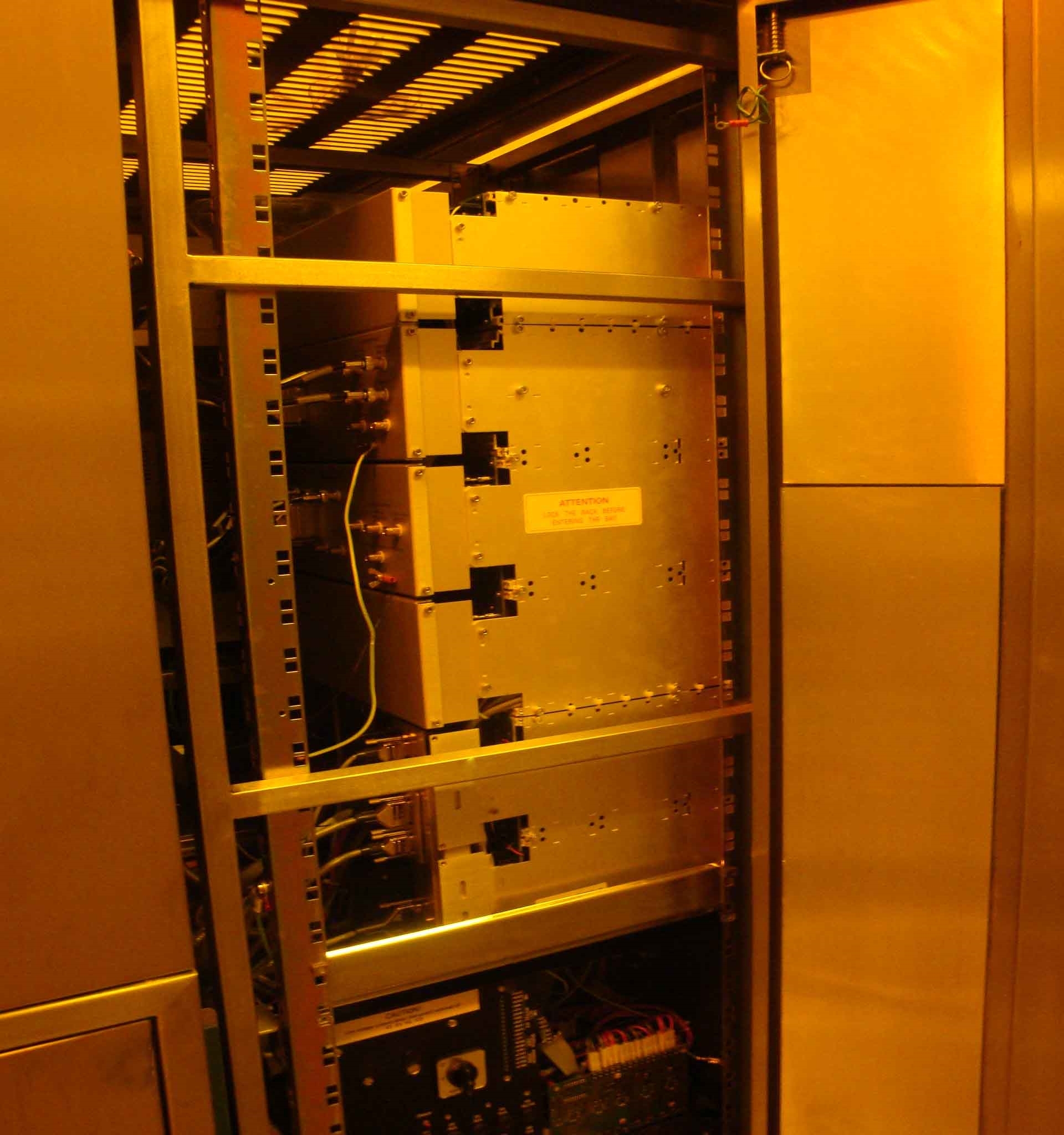
Scanning Electron Microscope (SEM), parts system
Needs detector and tip
Missing parts.
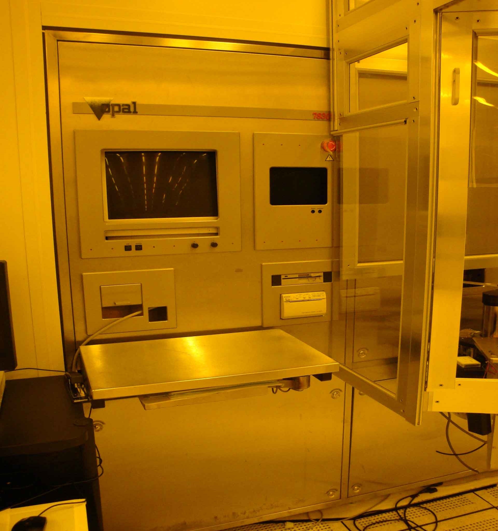
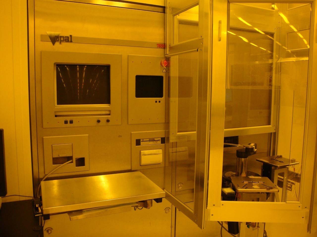
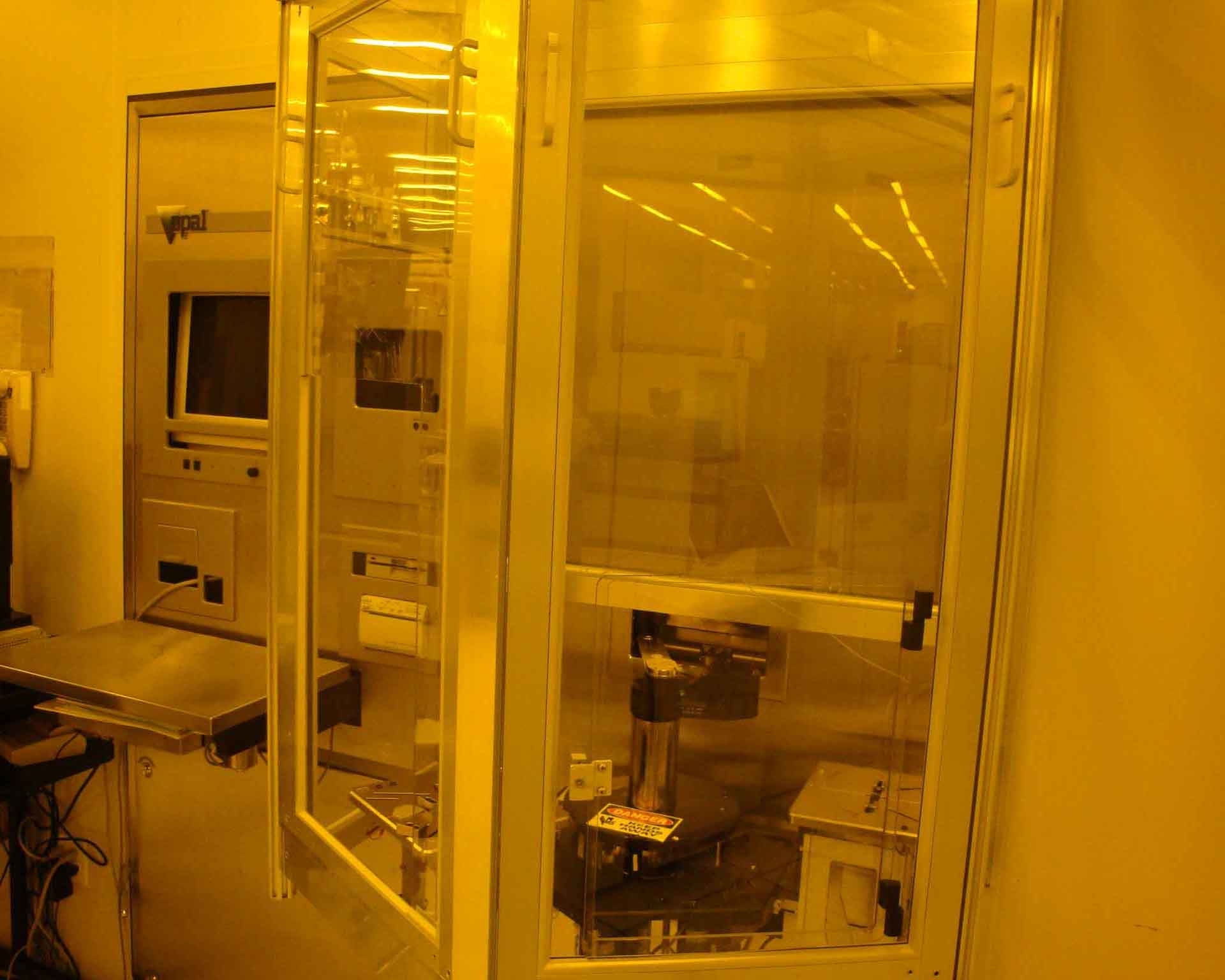
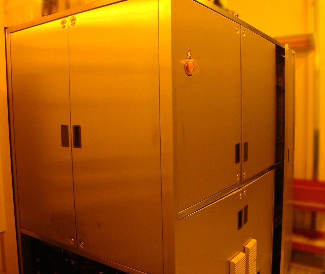
AMAT / APPLIED MATERIALS OPAL 7830I is an advanced scanning electron microscope (SEM) designed for precision imaging and analysis in the semiconductor industry. This equipment provides sub-nanometer resolution (with <4nm narrow size) and increased sensitivity for detailed observation that greatly surpasses traditional scanning technologies. The system has an analytical capability, with built-in focused ion beam (FIB) and electron beam lithography (EBL) capabilities. It provides both nano-scale sample preparation and visual analysis of objects buried in dense samples. This unit has a wide range of features including a high-precision 3-axis mechanical stage, a large dynamic range digital detector, and cutting-edge electron optical systems. This state-of-the-art machine allows for fine-tuning of both the beam energy and spot size to meet a customer's specific imaging needs. AMAT OPAL 7830I has a high-resolution field emission gun (FEG) that provides a stable electron beam with improved energy resolution and spot size. It has an in-built energy filter control that helps in selecting the right energy for imaging. The electron optics systems have adjustable astigmatism and spherical aberration for fine tuning. The electron optical tool has a large eyepiece and adjustable contrast controls to maximize image quality. The asset has integrated hardware, software and firmware components, all of which allow for stability and optimum performance. The model has a rapid high-precision sample stage and a digital CCD camera, allowing for accurate observation at the sub-nanometer level. Additionally, the FIB has a specially designed wave generator to allow for in-situ deposition and etching. The wide dynamic range CCD detector setup offers unmatched sensitivity and contrast. In this way imaging is improved compared to earlier imaging systems. APPLIED MATERIALS 7830I can be easily combined with CAD systems and automated robotic sample handling, allowing for high throughput and repeatable results. The equipment has automated features that reduce setup time and provide improved accuracy. On board scripting technology allows customers to customize their tests and increase the speed of work processes. Last but not least, the software allows for integration to other imaging applications such as electron backscatter diffraction (EBSD) and energy dispersive x-ray (EDS). These features allow APPLIED MATERIALS OPAL 7830I to deliver high-resolution imaging capabilities while maintaining the reliability and high precision that the semiconductor industry requires. It is the most advanced scanning electron microscope in today's market, providing superior imaging and analysis for the most demanding of industrial projects.
There are no reviews yet
