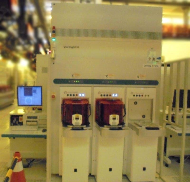
Used AMAT / APPLIED MATERIALS VeritySEM 2 #9094373 for sale
It looks like this item has already been sold. Check similar products below or contact us and our experienced team will find it for you.
Tap to zoom


Sold
ID: 9094373
Wafer Size: 12"
Vintage: 2003
Critical Dimension Scanning Electron Microscope (CD-SEM), 12"
Includes:
Thermally assisted field emission electron gun
Patented electron optics (YAP detector included)
SEM Autofocus and auto stigmation module
(3) Open cassette ports, 12"
Standing / Sitting operator console
3D Sidewall imaging
Signal tower
Thermal video and alphanumeric printers
Central recipe database server
Metrology
Lines and CH slope: (2) Angle, (2) Height
Repeatability: L-0.45 nm, CH-0.55 nm (1) 1°/ 1° / 1° 10 nm / 10nm / 17nm
Reproducibility: L-0.45 nm, CH-0.55 nm (1) 1° / 1° / 1° 10 nm / 10nm / 17nm
VeritySEM2: 0.9 nm
Imaging:
Image resolution: 1.65 nm at (4) 800, 0 V
Side wall imaging: (5) 15° Tilt at 4 directions
HAR Imaging: 1:30 Features
(7) ABW: 10.5 nm
Accelerating voltage: 0.2 kV - 2.5 kV
Extraction voltage up to 4 kV
Probe current: 5 pA - 500 pA
System performance:
Throughput: (6) Lines / Spaces slope / Height
5 Sites / Wafer: 65 WPH 13 WPH
20 Sites / Wafer: 33 WPH
PR Success rate: 99.70%
MTBF: 1,000 Hours
MTTR: 4 Hours
MTBA: 24 Hours
Availability: 95%
Wafer particle contamination:
Front 0.09 um particles 25 PWP / Wafer (With mini environment)
Front 0.2 um particles 5 PWP / Wafer (With mini environment)
Back 0.2 um particles 3000 PWP / Wafer (With mini environment)
Equipment parameters:
Wafer size: 6"-12"
Optical magnification 16x, 220x (FOV: 450 mm - 6000 mm)
SEM magnifications: 1,000x to 400,000x (100 mm - 0.25 mm)
Stage: 300 mm/s With continuous motion trackball
Host: 19.4 CBM
FFU: 2.0 CBM
Workstation: 2.5 CBM
UPS, Chiller and electric disk: 2.1 CBM
Does not include dry pump
2003 vintage.
AMAT / APPLIED MATERIALS VeritySEM 2 is a scanning electron microscope (SEM) used for the analysis of materials and surfaces. It enables the user to observe, characterize, and manipulate samples on the nanoscale. This powerful and versatile instrument is an invaluable tool for research and development purposes. The system consists of several basic subsystems including the electron gun, sample holder, electron optics, and detector. The electron gun generates a beam of electrons which are then focused and scanned over the surface of the sample. The sample holder is used to locate and position the sample for the electron beam. The electron optics are responsible for focusing the electrons onto the surface of the sample as well as their magnification and detection. The detector is used to analyze the electrons that are scattered from the sample. AMAT VeritySEM 2 is a highly precise and versatile instrument, allowing the user to conduct a wide range of analyses. With its ability to achieve magnifications up to 50,000x, APPLIED MATERIALS VERITY SEM 2 is an ideal tool for studying nanoscale features. The Sputter Ion Source option additionally allows for surface structuring and sputter etching. This feature allows manipulation of the sample surface at the nanoscale, such as deposition or removal of films, sputter etching, sputter cleaning, and patterning. VERITY SEM 2 also features a broad range of analytical capabilities. Its energy dispersive x-ray spectroscopy (EDS) option allows elemental characterization of the sample, and its energy-filtered imaging allows the user to precisely image different chemical and structural features with nanoscale resolution. The system also offers the capability to perform backscattered electron imaging, which allows for convincing visual inspection of material's surface features. In conclusion, VeritySEM 2 is a powerful and versatile instrument, suited for both materials characterization and manipulation of sample surfaces. Its ability to resolve nanoscale features, as well as its broad range of analytical capabilities, make it an effective tool for research and development.
There are no reviews yet