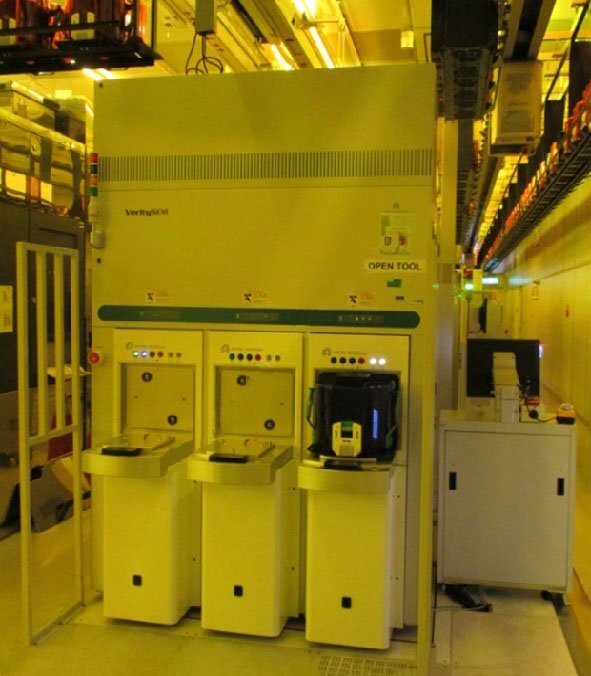
Used AMAT / APPLIED MATERIALS VeritySEM 2 #9359397 for sale
It looks like this item has already been sold. Check similar products below or contact us and our experienced team will find it for you.
Tap to zoom


Sold
ID: 9359397
Wafer Size: 6"-12"
Vintage: 2004
Critical Dimension Scanning Electron Microscope (CD-SEM), 6"-12"
Upgraded from VeritySEM
Hard Disk Drive (HDD) not included
Thermally assisted field emission electron gun
Patented electron optics (Including YAP Detector)
SEM Autofocus and autostigmation module
(3) Open cassette ports, 12"
Standing / Sitting operator console
3D Sidewall imaging
Signal tower
Central recipe database server (Tower type)
Repeatability:
Lines and CH-L-0.45nm CH-0.55nm
Slope angle STI/DD / Litho: 1deg / 1deg / 1deg
Height STI / D.Dam / Litho: 10nm / 10nm / 17nm
Reproducibility:
Lines and CH L-0.45nm CH-0.55nm
Slope angle STI / DD / Litho: 1deg / 1deg / 1deg
Height STI / D.Dam / Litho: 10nm / 10nm / 17nm
Matching: Lines and CH 0.9nm
Imaging:
Image resolution: 1.65 nm at 8000 V
Side wall imaging: 15 ° tilt at 4 directions
HAR Imaging: 1:30 Features
ABW: 10.5 nm
Accelerating voltage: 0.2 kV to 2.5 kV
Extraction: Up to 4 kV
Probe current: 5 pA - 500 pA
Throughput:
5 Sites / Wafer: Lines / Spaces 65 WPH
Slope / Height 13 WPH
20 Sites / Wafer: Lines / Spaces 33 WPH
MTBF: 1,000 hours
MTTR: 4 hours
MTBA: 24 hours
Availability: 0.95
Wafer particle contamination:
Front 0.09 um particles: 25 PWP / Wafer
Front 0.2 um particles: 5 PWP / Wafer
Back 0.2 um particles: 3000 PWP / Wafer
Carbonization: 0.05 nm per visit
Parameters:
Optical magnification: 16x, 220x
SEM Magnifications: 1,000x to 400,000x
Stage: 300 mm/s
With continuous motion trackball
2004 vintage.
AMAT / APPLIED MATERIALS VeritySEM 2 scanning electron microscope is a high resolution equipment used for analyzing nanoscale features on a variety of materials. The device is equipped with a field emission gun (FEG) electron source that produces a focused, high-energy beam of electrons, which is used to image and analyze objects at nano-scale resolution. The instrument comes with a full suite of hardware, software, and options that enable it to function as an imaging device, analytical platform, and even an imaging-based material characterization system. AMAT VeritySEM 2 is capable of producing an image with a resolution of up to 50 nm, and with a depth of view of up to 10 µm. This makes it well-suited for the study of ultra-fine features and structures. Its high resolution makes it ideal for imaging, analyzing, and characterizing materials at the nanoscale. The instrument has an acceleration voltage range of 0.3 to 30 kV, which makes it capable of operating at various magnifications and depths. It is also equipped with an in-lens unit that allows for the study of dynamic processes such as the effects of acceleration voltage and image processing. APPLIED MATERIALS VERITY SEM 2 is complemented with a range of accessories including an EDS detector, an EBSD detector, an edge detector, and a cryo-stage. The EDS and EBSD detectors enable the user to perform elemental and crystallographic analysis, respectively. The edge detector is ideal for locating minute structural features and uneven surfaces. The cryo-stage enables the user to observe specimens in a cryogenic environment. VERITY SEM 2 can be controlled remotely using the machine's touchscreen or via computer. Additionally, its remote graphical user interface offers access to a variety of settings. This on-screen control and reporting machine makes it easier for the user to obtain the desired results in less time. AMAT VERITY SEM 2 is a powerful and highly configurable scanning electron microscope that provides a range of features and benefits. Its high resolution imaging, crystal analysis capabilities, and in-lens process control make it an indispensable tool for nanoscale imaging and analysis.
There are no reviews yet